Halmstad University Post-Print
Modular Interconnection System for
Optical PCB and Backplane
Communication
Sacki Agelis, Sofia Jacobsson, Magnus Jonsson, Arne Alping and
Per Ligander
N.B.: When citing this work, cite the original article.
©2002 IEEE. Personal use of this material is permitted. However, permission to reprint/republish this material for advertising or promotional purposes or for creating new collective works for resale or redistribution to servers or lists, or to reuse any copyrighted component of this work in other works must be obtained from the IEEE.
Agelis S, Jacobsson S, Jonsson M, Alping A, Ligander P. Modular interconnection system for optical PCB and backplane communication. In: Proceedings:
International Parallel and Distributed Processing Symposium : April 15-19, 2002, Ft. Lauderdale, Florida, USA. Los Alamitos, Calif.: IEEE; 2002. p. 245-250. DOI: http://dx.doi.org/10.1109/IPDPS.2002.1016665
Copyright: IEEE
Modular Interconnection System for Optical PCB and Backplane Communication
Sacki Agelis
1, Sofia Jacobsson
1, Magnus Jonsson
1, Arne Alping
2, and Per Ligander
21. School of Information Science, Computer and Electrical Engineering, Halmstad University,
Halmstad, Sweden, Box 823, S-301 18, Sweden. Magnus.Jonsson@ide.hh.se, http://www.hh.se/ide
2. Ericsson Microwave Systems, Mölndal, Sweden
Abstract
This paper presents a way of building modular systems with a powerful optical interconnection network. Each module, placed on a Printed Circuit Board (PCB), has a generic optical communication interface with a simple electronic router. Together with optical switching using micro-electromechanical system (MEMS) technology, packet switching over reconfigurable topologies is possible. The interconnection system gives the possibility to integrate electronics with optics without changing existing PCB technology. Great interest from industry is therefore expected and the cost advantages are several: reuse of module designs, module upgrades without changing the PCB, low-cost conventional PCB technology, etc. In the version described in this paper, the interconnection system has 48 bidirectional optical channels for intra-PCB communication on each board. For inter-PCB communication, a backplane with 192 bidirectional optical channels supports communication between twelve PCBs. With 2.5 Gbit/s per optical channel in each direction, the aggregated intra-PCB bit rate is 120 Gbit/s full duplex (on each PCB) while the aggregated inter-PCB bit rate is 480 Gbit/s full duplex. A case study shows the feasibility of the interconnection system in a parallel processing system for radar signal processing.
1 Introduction
Today’s Printed Circuit Boards (PCBs) are concerned with high design efforts in the sense that a unique construction must be developed for each version. In financial terms this is very expensive and due to this, it is desirable to get a modular way of system design, where modules placed on the PCBs have a generic communication interface. The increasing demand for bandwidth suggests that optics should be used for the interconnections. Optical interconnects not only allow higher throughputs but also increase I/O density, improve electromagnetic compatibility and simplifies cable solutions compared to traditional electrical solutions. These benefits strongly
suggest that some form of optical interconnections should be used for intra-PCB and inter-PCB communication.
This paper presents a way of building modular systems on a PCB, where modules (e.g. multi-chip modules or daughter PCBs) communicate with each other through optical interconnections and optical switches. Each optical switch is a micro-electromechanical system (MEMS) with an array of 32×32 mirrors. An aggregated intra-PCB bit rate of 120 Gbit/s is possible in the system. Each module has a generic communication interface with an internal simple electrical router. Fiber-ribbons are used to connect the modules and the optical switches.
Our proposed system also includes an optical backplane. Several free-space optical backplanes has been proposed in the litterature [1-4]. Compared to these, we propose the use of a passive fiber-optic backplane without the need for additional opto-electronic components to interface with the backplane. In other words, the backplane fits very well together with the PCB communication system. The passive optical backplane is based on the fiber-foil technology [5] [6] [7], which recently has become commercially available. For scalability reasons, the passive optical backplane can optionally be extended with optical switching. An aggregated backplane bit rate of 480 Gbit/s full duplex is supported for a backplane with twelve cards.
Our solution makes it possible to develop PCBs with optical interconnections between the modules and between the boards, without changing the manufacturing technology of the PCBs. Also, the MEMS technology used is suitable for mass production [8]. More information on all-optical switching is found in [9].
Other projects have proposed optical interconnections within small areas too, e.g., waveguides embedded in the PCBs [10], free-space communication between PCBs [11], and free-space communication between substrates in systems built in 3-dimensional space [12]. What distinguishes our proposed optical interconnection concept is that it offers: (i) a modular way of designing, (ii) a
reconfigurable topology at the same time as offering, (iii)
electronic routing that makes all modules reachable from each other, (iv) the possibility to use low-cost conventional
Agelis, S., S. Jacobsson, M. Jonsson, A. Alping, and P. Ligander, “Modular interconnection system for optical PCB and backplane communication,” Proc. Workshop on Massively Parallel Processing (WMPP'02) in conjunction with International Parallel and Distributed Processing Symposium (IPDPS'02), Fort Lauderdale, FL, USA, April 19, 2002.
PCB technology, (v) compact rack-based systems with
15-20 mm PCB pitch, (vi) a generic communication interface
for the modules, (vii) system-wide optical interconnections
including both PCBs and backplane, and (viii) powerful
optical switching suitable for mass production. A case study shows the feasibility of using the architecture for future demanding radar signal processing. Other application areas include data- and telecommunication switch equipment, radio base station signal processing, and other embedded parallel processing applications.
The rest of the paper is organized as follows. Section 2 presents the board-level system architecture. In Section 3, two backplane systems are described. The case study is then presented in Section 4. The paper is concluded in Section 5.
2 Board-level interconnection architecture
Below, the board-level interconnection system is described, beginning with physical parameters (Section 2.1). Then, in Section 2.2, the optical interconnections are presented, followed by a discussion of topologies and routing in Section 2.3.
2.1 Physical parameters
Basically the configuration of one PCB is composed of six modules on each side, as shown in Figure 1a, where each module has four optical channels connected to the switch on the same PCB side. In turn, each of the two switches on a PCB has eight optical channels connected to the backplane. In other words, the two PCB sides has an identical interconnection architecture, as clarified in Figure 1b. Each optical channel is assumed to have a bit rate of 2.5 Gbit/s.
Each module on a PCB has a size of 65×65 mm. The
PCB has an area of 200×300 mm and an inter-PCB distance in the rack of approximately 15 to 20 mm. This leads to a maximum height of the devices mounted on the board of 7 mm on each side of the PCB. PCBs with sizes smaller than 200×200 mm and modules possibly smaller
than 65×65 mm are planned but are not treated in this
paper. In addition to the generic communication interface, each module can contain, e.g., memory, one or several processing units, and other necessary devices to handle basic control flows and power dependencies.
2.2 Optical interconnections
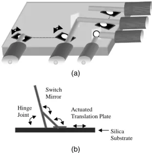
The optical switches used consist of pop-up MEMS with 32×32 mirrors. The actuated free-routing mirrors are monolithically integrated on a silicon chip. By pushing a selected mirror, the collimated light is switched to desired output port. This is shown in Figure 2a. The micro-actuated free-routing switch mirror consists of a mirror that is anchored on the substrate and is connected to the translation stage by push rods, as shown in Figure 2b. The translation stage is actuated by arrays of scratch-drive actuators. This technology is seen to achieve low light-loss, low crosstalk, and low polarization dependence as described in [13]. The size of each mirror is 150×140 µm
and the distance between them has to be at least 500 µm. A disadvantage with this technology is the relatively long switching time, which is less than 700 µs [14]. However, one can easily reconfigure the topology with the optical switch during run-time, which makes it possible to, e.g., adapt to the current data flow between the modules (see Section 2.3). A similar MEMS based optical switch is described in [15].
Fiber-ribbons connect the MEMS based switch and the modules (see Figure 3). This structure is also applied between the backplane and the switch. Another possibility is to encapsulate these fiber highways and laminate them within a plastic foil for easy mounting and coupling to its connectors. The fibers would then not have to wear their surrounding jackets and all the fibers would lie in one
(a) (b)
Figure 1: (a) Top view of the PCB configuration. (b) side view of the PCB configuration.
(a)
Hinge
Joint ActuatedTranslation Plate Switch
Mirror
Silica Substrate
(b)
Figure 2: (a) A 32×32 optical switch with pop-up mirrors. (b) Outline of a pop-up mirror.
plane. The optical switch is connected to six fiber-ribbons (through the same socket) with a total of 24 optical channels in each direction on the board side, and to one fiber-ribbon with eight optical channels in each direction on the backplane side. In other words, one fiber-ribbon with four fibers in each direction is used for the connection of each module with the optical switch. In total, the switch has 32 input channels and 32 output channels and is a non-blocking switch.
The generic communication interface of the module has four vertical cavity surface-emitting lasers (VCSEL) and four photo-detectors, i.e., interfacing to four bidirectional optical channels. A VCSEL converts an electrical signal to a light beam and transmits it across a fiber link to the MEMS switch, where the light beam is switched to a proper receiver channel, finally hitting the photo-detector in the receiving module where the light is converted back to an electrical signal. Observe that the interconnection between two arbitrary modules is completely of optical nature, outside the module. Low-cost VCSELs with a wavelength of 850 nm and with a maximum bit rate of 2.5 Gbit/s are assumed.
2.3 Reconfigurable optical topologies with
electronic routing
Interconnection topologies are divided into two groups, dynamic and static. In our solution, a static topology has been chosen due to the fact that the optical switch has long switching times. However, as mentioned above, the topology can be reconfigured in less than a millisecond by changing the state of the pop-up mirrors. Examples of topologies that can be embedded on a PCB are ring and mesh. If using the ring topology, four fibers can be grouped together to form a 10 Gbit/s unidirectional ring. Another possible configuration is to have two rings, one 5 Gbit/s ring in each direction.
Traffic can always be routed to the final destination by passing several modules in the topology since the
communication interface in each module is equipped with an electronic router (see Figure 4). Source routing and through switching [16] are assumed to be used. With cut-through switching, only the header of the packet (with the destination address) has to arrive before the packet can be forwarded to an output port. This means that the router do not have to store the whole packet as long as the output port is free. A schematic view of the system on one PCB side is shown in Figure 5, where M denotes a module
associated with its own routing function and its four bidirectional optical channels.
3 Backplane communication
Below, two optical backplane solutions to connect the PCBs and obtain a system-wide interconnection system are presented (see Figure 6). The first solution is a passive optical one, while the second extends the passive optical backplane with optical switching.
Figure 3: Fiber-ribbons connect the modules on a PCB side to the switch, and the switch to the backplane. Photo-diodes Electronic Router 1 2 3 4 VCSEL array 1 2 3 4 Fiber-ribbon to the optical switch
Interface to the application specific part of the module
Figure 4: Generic communication interface with
four VCSELs, four photo-diodes, and an
electronic router.
Routing
function
Optical Interconnection using MEMSM
B A C K P L A N E S Y S T E MM
M
M
M
M
Figure 5: Schematic view of the MEMS switch and the modules on one PCB side.
3.1 Passive optical backplane
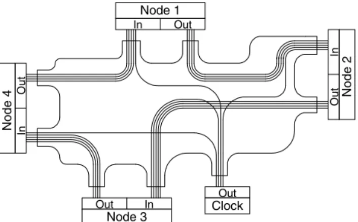
Fibers or other kinds of waveguides (hereafter commonly denoted as channels) can be integrated to form a more or less compact system of channels. Fibers can be laminated to form a foil of channels, for use as intra-PCB or back-plane interconnection systems [5] [6] [7]. Fiber-ribbon connectors are applied to fiber end-points of the foil. An example is shown in Figure 7, where four nodes are connected in a ring topology, the medium is simply changed into an even more compact variant of the fiber-ribbon ring network [17]. In addition, there is a clock that distributes clock signals to the four nodes via equal-length fibers to keep the clock signals in phase. In other words, a fiber-optic clock distribution network and a data network are integrated into one system. Using polymer waveguides instead of fibers brings advantages such as the potential for more cost-effective mass production [5].
In the proposed system, the two optical switches on each PCB are passively connected to a backplane foil via fiber-ribbon cables. The interconnection topology in the backplane foil can be arbitrarily chosen but is here assumed to be a unidirectional multi-fiber ring as seen in Figure 8. Of course, a quite similar and sometimes better possible topology is to split the eight parallel channels into two bidirectional rings, each with four parallel channels. Another possible topology is the torus, e.g., connecting the 24 sides of twelve PCBs into a 6×4 node 2-dimensional torus. In other words, one can design the backplane and configure the switches on the PCBs to get a regular system-wide topology with, e.g., 144 modules distributed on twelve PCBs.
3.2 Optical backplane and switch card
In the MEMS switches assumed above, the optical beams moves in 2-dimensional space where each mirror is controlled to be in either down-position (no beam bounce)
or up-position (beam bounce). This brings compact solutions for small or medium-sized switches. The disadvantage with the 2-dimensional MEMS switch is that
N2mirrors are needed in an N×N switch. A more scalable solution is to let the beams travel in 3-dimensional space and to use mirrors for which the angle can be controlled in two axis. In anN×N switch, two arrays of size√N×√N are
used. Each beam will first bounce on an input specific mirror in the first array and then on an output specific mirror in the second array. Lucent Technologies has already announced 256×256 switches based on the 3-dimensional MEMS technology to be released on the market [18]. Due to the relatively low loss possible in MEMS switches, multistage MEMS switches are also possible. In this way, rather large optically transparent switches can be built.
With a 32×32 switch on each side of each PCB as described above, we have eight bidirectional channels connecting each PCB side to the foil backplane. Assuming twelve PCBs, a single 192×192 3-dimensional optical MEMS switch is needed to get a fully reconfigurable backplane topology. The passive fiber-optic foil is then
Figure 6: Rack-based system with PCBs
connected by a backplane, in this case optical.
Node 3 N ode 4 Node 2 Node 1 Clock Out In In Out In O u t Ou t In Out
Figure 7: A foil of fibers connects four nodes and distributes clock signals to them.
made to connect each board to the backplane switch. The aggregated backplane bit rate is 480 Gbit/s full duplex. The backplane switch can be placed, e.g., behind the PCBs and the foil. Another solution is to replace two ordinary PCBs with a PCB holding the backplane switch. Two PCB slots are expected to offer enough room for the height of the 3-dimensional MEMS system.
4 Case study
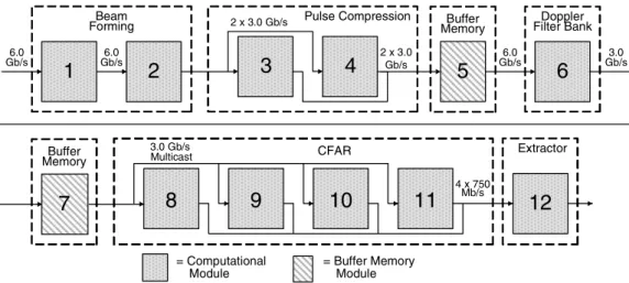
A typical application with high throughput requirements between the computational modules is future radar signal processing systems. In Figure 9, a signal processing chain similar to those described in [19] and [20] is shown together with its bandwidth demands. Each computational module in the figure contains multiple processors itself [21]. For simplicity, we have chosen a signal processing chain that fits exactly on the twelve modules on a double-sided PCB. A similar case study for a whole rack can also be made but is not treated here. Each 2.5 Gbit/s channel is
assumed to have a usable bit rate for the data flow in the signal processing chain of 1.5 Gbit/s, allowing for overhead, control traffic, logging etc. This means that four incoming channels from the backplane, with the radar data, gives the needed 6 Gbit/s.
The chain with its pipelined dataflow is a good example containing both multicast, one-to-many, and many-to-one communication patterns. The aggregated throughput demand is nearly 40 Gbit/s. We leave out all details of the chain, referring to the two other papers, and do only treat the throughput demands here. A feasible interconnection topology configured by the MEMS switches and the multi-fiber backplane ring is shown in Figure 10. The incoming dataflow to the CFAR (Constant False Alarm Ratio) nodes is multicasted to all these nodes. This is done by multicasting to two nodes two times, each with one electronic routing hop. These two multicasts are the only parts in the signal processing chain where electronic routing is needed. However, electronic routing is needed for, e.g., control traffic to pass several hops. If the radar system changes working mode during run-time, the switches can easily be reconfigured to adapt to the new signal processing chain.
5 Conclusions
In this paper, we have proposed a complete interconnection system for optical communication for both intra- and inter-PCB communication. Our solution makes it possible to develop PCBs with optical interconnections between modules on the PCBs and between the boards, without changing the manufacturing technology of the PCBs. The communication system supports both optically reconfigurable topologies and electronic routing to offer high flexibility and high performance at the same time. Also worth mentioning is that the MEMS technology used is suitable for mass production.
Beam Forming 6.0 Gb/s 3.0 Gb/s Multicast 4 x 750 Mb/s 3.0 Gb/s Extractor CFAR = Computational Module = Buffer Memory Module Doppler Filter Bank Buffer Memory 2 x 3.0 Gb/s Pulse Compression 2 x 3.0 Gb/s Buffer Memory 6.0 Gb/s Gb/s6.0
1
2
3
4
6
8
9
10
11
12
7
5
Figure 9: Data flow between the modules in the radar signal processing chain.
Top side MEMS based switch
1
2
3
4
5
6
Bottom side MEMS based switch
7
8
9
10
11
12
2 2 2 2 2 4 4 2 2 2 2 4 Bac k p laneFigure 10: Mapping of the signal processing chain on one PCB with twelve modules.
References
[1] C. Zhao, J. Liu, and R. T. Chen, ”Hybrid optoelectronic backplane bus for multiprocessor-based computing systems,”
Proc. 3rd International Conference on Massively Parallel Processing using Optical Interconnections (MPPOI’96), Maui,
HI, USA, Oct. 27-29, 1996, pp. 313-320.
[2] B. Supmonchai and T. Szymanski, "High speed VLSI concentrators for terabit intelligent optical backplanes," Proc. Optics in Computing (OC'98), Brugge, Belgium, June 17-20,
1998, pp. 306-310.
[3] K. Hirabayashi, T. Yamamoto, and S. Hino, “Optical backplane with free-space optical interconnections using tunable beam deflectors and a mirror for bookshelf-assembled terabit per second class asynchronous transfer mode switch,” Optical Engineering, vol. 37, no. 4, pp. 1332-1342, Apr. 1998.
[4] K. Hamanaka, “Optical bus interconnection system using selfloc lenses,” Optics Letters, vol. 16, no. 6, pp. 1222-1224,
Aug. 15, 1991.
[5] P. Eriksen, K. Gustafsson, M. Niburg, G. Palmskog, M. Robertsson, and K. Åkermark, "The Apollo demonstrator−new low-cost technologies for optical interconnects," Ericsson Review, vol. 72, no. 2, 1995.
[6] M. Robertsson, K. Engberg, P. Eriksen, H. Hesselbom, M. Niburg, and G. Palmskog, "Optical interconnects in packaging for telecom applications," Proc. of the 10th European Microelectronics Conference, pp. 580-591, 1995.
[7] M. A. Shahid and W. R. Holland, ”Flexible optical backplane interconnections,” Proc. 3rd International Conference on Massively Parallel Processing using Optical Interconnections (MPPOI’96), Maui, HI, USA, Oct. 27-29, 1996, pp. 178-185.
[8] A. Neukermans and R. Ramaswami, “MEMS technology for optical networking applications,” IEEE Communications Magazine, vol. 39, no. 1, pp. 62-69, Jan. 2001.
[9] A. Pattavina, M. Martinelli, G. Maier, and P. Boffi, “Techniques and technologies towards all-optical switching,”
Optical Networks Magazine, vol. 1, no. 2, pp. 75-93, Apr. 2000.
[10] E. Griese, “A high performance hybrid electrical-optical interconnection technology for high-speed electronic systems”,
IEEE Transactions On Advanced Packaging, vol. 24, no. 3, pp.
375-383, Aug. 2001.
[11] D. V. Plant, M. B. Venditti, E. Laprise, J. Faucher, K. Razavi, M. Châteaunuef, A. G. Kirk, and J. S. Ahearn, “256-channel bidirectional optical interconnect using VCSELs and
photodiodes on CMOS”, IEEE Journal of Lightwave Technology, vol. 19, no. 8, pp. 1093-1103, Aug. 2001.
[12] J. A. Neff, ”Optical interconects based on two-dimensional VCSEL arrays,” Proc. Massively Parallel Processing using Optical Interconnections (MPPOI’94), Cancun, Mexico, Apr.
26-27, 1994, pp. 202-212.
[13] L. Y. Lin, E. L. Goldstein and R. W. Tkach, “Free-space micromachined optical switches for optical networking,“ IEEE Journal of Selected Topics in Quantum Electronics, vol. 5, no. 1,
pp. 4-9, Jan./Feb. 1999.
[14] L. Y. Lin, E. L. Goldstein and R. W. Tkach, “Free-space micromachined optical switches with submillisecond switching time for large-scale optical crossconnects,“ IEEE Photonics Technology Letters, vol. 10, no. 4, pp. 525-527, April. 1998.
[15] P. M. Hagelin, U. Krishnamoorthy, J. P. Heritage, and O. Solgaard, “Scalable optical cross-connect switch using micromachined mirrors,” IEEE Photonics Technology Letters,"
vol. 12, no. 7, pp. 882-884, July 2000.
[16] P. Kermani and L. Kleinrock, “Virtual cut-through: a new computer communication switching technique,” Computer Networks, vol. 3, pp. 267-286, 1979.
[17] M. Jonsson, “Two fiber-ribbon ring networks for parallel and distributed computing systems,” Optical Engineering, vol.
37, no. 12, pp. 3196-3204, Dec. 1998.
[18] M. Kenward, "Mirror magic ushers in the all-optical network,"Fibre Systems, pp. 37-39, May 2000.
[19] M. Taveniku, A. Åhlander, M. Jonsson, and B. Svensson, “A multiple SIMD mesh architecture for multi-channel radar processing,” Proc. International Conference on Signal Processing Applications & Technology, ICSPAT´96, Boston,
MA, USA, Oct. 7-10, 1996, pp. 1421-1427.
[20] M. Jonsson, A. Åhlander, M. Taveniku, and B. Svensson, “Time-deterministic WDM star network for massively parallel computing in radar systems,” Proc. Massively Parallel Processing using Optical Interconnections, MPPOI’96, Lahaina,
HI, USA, Oct. 27-29, 1996, pp. 85-93.
[21] M. Taveniku, A. Ahlander, M. Jonsson, and B. Svensson, "The VEGA moderately parallel MIMD, moderately parallel SIMD, architecture for high performance array signal processing," Proc. 12th International Parallel Processing Symposium & 9th Symposium on Parallel and Distributed Processing (IPPS/SPDP’98), Orlando, FL, USA, Mar. 30 - Apr.