http://www.diva-portal.org
Postprint
This is the accepted version of a paper published in Journal of Applied Physics. This paper
has been peer-reviewed but does not include the final publisher proof-corrections or journal
pagination.
Citation for the original published paper (version of record):
Adamczyk, K., Søndenå, R., Stokkan, G., Looney, E., Jensen, M. et al. (2018)
Recombination activity of grain boundaries in high-performance multicrystalline Si
during solar cell processing
Journal of Applied Physics, 123(5): 055705-1-055705-6
Access to the published version may require subscription.
N.B. When citing this work, cite the original published paper.
Permanent link to this version:
1
Recombination activity of grain boundaries in high-performance
multicrystalline Si during solar cell processing
Krzysztof Adamczyk
*,1, Rune Søndenå
2, Gaute Stokkan
3, Erin Looney
4, Mallory Jensen
4, Barry Lai
5,
Markus Rinio
6, and Marisa Di Sabatino
11 Department of Materials Science and Engineering, NTNU, A. Getz vei 2B, NO-7491 Trondheim, Norway 2 Department for Solar Energy, IFE, NO-2007 Kjeller, Norway
3 SINTEF Materials and Chemistry, NO-7465 Trondheim, Norway 4 Massachusetts Institute of Technology, Cambridge, MA 02139, USA
5 Advanced Photon Source, Argonne National Laboratory, Lemont, IL 60439, USA 6 Karlstad University, 651 88 Karlstad, Sweden
In this work, we applied internal quantum efficiency mapping to study the recombination activity of grain boundaries in High Performance Multicrystalline Silicon under different processing conditions. Wafers were divided into groups and underwent different thermal processing, consisting of phosphorus diffusion gettering and surface passivation with hydrogen rich layers. After these thermal treatments, wafers were processed into heterojunction with intrinsic thin layer solar cells. Light Beam Induced Current and Electron Backscatter Diffraction were applied to analyse the influence of thermal treatment during standard solar cell processing on different types of grain boundaries. The results show that after cell processing, most random-angle grain boundaries in the material are well passivated, but small-angle grain boundaries are not well passivated. Special cases of coincidence site lattice grain boundaries with high recombination activity are also found. Based on micro X-ray fluorescence measurements, a change in contamination level is suggested as the reason behind their increased activity.
1 Introduction
With multicrystalline silicon being the dominant material used for solar cells, the mechanisms of how crystalline defects affect final device performance require more attention 1,2. It is established that both dislocations
and grain boundaries are detrimental in this regard 3-6 due to the interactions between these structural defects and
impurities introduced to the material at various process stages 3,7. It was reported that the increased recombination
strength of dislocations during solar cell processing can be related to a change in precipitate distribution 8. In the
so called High Performance Multicrystalline (HPMC) silicon, material grain boundaries are an important part of the structure. Traditionally grain boundaries were considered as harmful to device performance, and crystal growth processes were optimized to obtain large grains with small grain boundary densities. Recently it was discovered that decreasing the grain size while maintaining a structure where random-angle grain boundaries (RAGB) were prevalent led to increased cell efficiency 9-11. RA grain boundaries allow a better relaxation of thermal stress, acting
as sinks for recombination active dislocations. The second type of grain boundaries most often found in HPMC Si are the Coincidence Site Lattice (CSL) grain boundaries withΣ3 index of coincidence 11. Most of the Σ3 grain
boundaries are coherent twin boundaries, meaning that the interface plane has the same orientation of the {111} type in the two adjacent grains 12. Grain boundaries, where the grains still have a CSL orientation relative to each
other, but where the boundary plane is random, can also occur. Because of the orientation of the plane in such cases, the resulting boundary often consists of small facets coherent on their own. Some cases of such Σ3 grain boundaries consist of facets with {111} and {112} orientations, and the {112} facets introduce a lattice mismatch relaxed by an extended bond of a silicon atom with 5-fold-coordination 13. Cases of macroscopically incoherent
Σ3 grain boundary planes with a random plane orientation, but microscopically coherent {111} and {112} facets with a neighboring array of dislocations were also found 14. Small-angle grain boundaries (SAGB), i.e., grain
boundaries with their misorientation angle below 15°, can be also found in the material. This type of grain boundary is structurally equivalent to a line of densely-packed dislocations. According to Chen and Sekiguchi, this type of grain boundary is the most detrimental to the electrical performance 15.
The focus of this work is to study the different types of grain boundaries in HPMC Si, and to quantify the effects of different thermal processes in standard solar cell manufacturing on the recombination activity at these grain boundaries, in order to better understand how they affect the final cell efficiency.
2
2 Experimental methods
2.1 Growth and processing The material used in this study comes from a hybrid ingot consisting of half
HPMC, and half Quasi-Mono (QM) material. The ingot has been grown in a Crystalox DS 250 furnace with a specific seeding structure allowing for simultaneous growth of HPMC and quasi-mono in one ingot. A high purity crucible was used to obtain purity in the ingot grown in a pilot scale furnace comparable with industrially grown ingots. A detailed description of the seeding structure can be found elsewhere 8,16. More information about wafer
processing and sample preparation can also be found therein, but the basic details are presented below.
The ingot was cut into a block, ground and industrially wafered into full size (156 x 156 mm²) wafers about 180 µm thick. The wafers were then damage etched. The first group consists of ungettered (U) wafers. The second group of wafers (G) was gettered by phosphorus in-diffusion at 830 °C with POCl3 gas for 60 minutes followed
by an emitter etch-back. The third group of wafers was gettered and subsequently hydrogenated through a simulated contact firing process with a hydrogen rich anti-reflection coating present prior to the emitter etch-back. This last group, after phosphorus diffusion gettering and a standard high temperature contact firing process with a peak temperature of 720 °C, constituted the gettered and hydrogenated group (G+H). All wafers were then surface passivated using PECVD deposition of hydrogenated amorphous silicon. The groups consisted of neighboring wafers, thus for each position in the ingot, the same grain boundaries were compared after different processing steps.
Processed wafers were cut to 50 mm × 50 mm samples and processed further into Heterojunction with Intrinsic Thin layer solar cells (HIT) 17. The cell structure enabled Light Beam Induced Current (LBIC) measurements, and
the HIT structure was chosen to avoid thermally induced changes to the bulk recombination activity thanks to the low processing temperatures (less than 200 °C). Following electrical characterization, the cell structure was removed by etching in aqua regia at 80 °C for 2 h. Samples were then mechanically polished to enable Electron Backscatter Diffraction (EBSD) analysis of grain boundaries. Finally, 10 mm × 10 mm samples were cut from several samples for Micro X-Ray Fluorescence (µ-XRF), to analyse the precipitate distribution in selected areas.
2.2 Characterization The main purpose of this work was to quantify the recombination activity of specific
grain boundaries at different process steps. To this end, LBIC was chosen as a technique to map the internal quantum efficiency (IQE) at grain boundaries with sufficient spatial resolution. The measurements of HIT cells made on the analysed wafers were performed using a custom-built LBIC system with a 826 nm laser as excitation source. The spatial resolution used was about 12.5 µm under about 2 µW light power 3,18. The recombination
activity at grain boundaries has been quantified using IQE contrast, according to the formula presented and used by Chen and Sekiguchi 15:
b
g
b
c
I
I
I
IQE
−
=
(1)Where Ib is the IQE of the background and Ig the IQE at the grain boundary.
After LBIC characterization, samples were prepared for EBSD measurements and analysed with a Nordif EBSD detector mounted on a Jeol JSM 840 microscope. The grain boundary type information was extracted from the resulting data using the “EDAX OIM Analysis” software. The restrictive Palumbo criterion was used to classify CSL grain boundaries 19,20. The resulting grain boundary maps and IQE maps were manually matched.
Spatially-resolved µ-XRF measurements were used to map metal distributions at grain boundaries in selected samples. These measurements were performed at beamline 2-ID-D at the Advanced Photon Source, using a 200 nm beam spot size and 220 nm steps to scan areas of about 225 µm2 and 400 µm221.
3 Results and discussion
The results presentation is divided into the bottom part of the ingot, and middle and top parts, as the grain boundaries in the bottom showed different electrical activity during processing, most probably because of a difference in initial impurity concentration. There was also a difference between the wafers coming from middle and top of the ingot, in that the grain boundaries in wafers from the top showed a stronger IQE contrast after gettering, but since the changes in contrast during processing and the characteristics of the fully processed, G+H group from the top were similar to what was observed in the middle, they are discussed in one section.
3.1 Bottom of the ingot Grain boundaries affect the IQE strongly in this part of the ingot, as the grain size
is smaller, meaning a larger grain boundary density. Figure 1 shows a representative sample area analyzed by IQE after different processing steps, and a corresponding EBSD map. These results suggest that at the bottom of the ingot, the recombination active grain boundaries are mostly of the RA and SA type, with CSL grain boundaries showing recombination activity less frequently.
3
Figure 1Representative IQE maps from the bottom of the ingot after different processing steps, compared to EBSD of the gettered sample (lower left). The black, horizontal lines in the IQE maps are the contact fingers. The white line in the IQE maps shows the position of the linescans discussed in Figure 2.
The ungettered state shows a much lower overall performance on samples from the bottom of the ingot. The IQE map reveals zones near grain boundaries with increased efficiency. The intragrain IQE is at levels of 60–70% and at the grain boundaries it is lower, down to 40–50%, but there is a zone up to about 100–150 µm from the grain boundary where the IQE increases even up to 80%. These zones with increased IQE can be explained based on an assumption that the overall poor performance of the ungettered samples is caused by an increased impurity concentration in this part of the ingot 22,23. The zone with increased IQE values would then be an area depleted of
impurities through internal gettering and precipitation on grain boundaries, so-called “denuded zones” 24. A
detailed analysis of such denuded zones was performed by Autruffe at el. 20. An important conclusion from their
work, relevant to the results presented here, is that precipitates in HPMC Si, in absence of dislocation clusters, form rather on sparse intra-granular dislocations than on grain boundaries. Additionally, the low dislocation densities in the material lead to higher interstitial iron concentration after solidification, because there are less nucleation sites present. These conclusions are directly comparable with the material from the bottom of the ingot presented here in the ungettered state. While lower IQE levels can be found directly on grain boundaries, cells made from such material are mostly limited by the low intragrain IQE. According to Autruffe et al. this would be caused by precipitation on the intragrain dislocations and by interstitial iron, present in the intragrain areas in higher concentration than in the denuded zones close to grain boundaries.
Figure 2 IQE profiles over the random-grain boundary marked with a white line in Fig. 1. from the bottom of the ingot after
different processing. No improvement in the IQE at the grain boundary is observed from gettering.
Phosphorus diffusion gettering improves the overall IQE considerably, but mainly through changing the impurity concentration in the bulk. This can be seen both in Figure 1 and when comparing the profiles in Figure 2. Only the intragrain IQE is increased, the IQE measured at the grain boundary remains at levels of about 50%, giving a stronger grain boundary contrast. The internal gettering occurring at grain boundaries is probably stronger than on the sparse intragrain dislocations. The grain boundaries, with a similar IQE as in the ungettered state, but with a higher bulk IQE show a stronger contrast and indicate, that in the absence of dislocation clusters the
4
impurities that are not extracted to the emitter by PDG most probably diffuse and decorate the random-angle and small-angle grain boundaries during the gettering process.
The majority of grain boundaries are passivated during the process of firing with deposited hydrogen-rich layers. As the profiles in Figure 2 indicate, the IQE contrast on grain boundaries is reduced during firing by reducing their recombination activity, but the high intragrain IQE is not changed. The IQE maps indicate, however, that some grain boundaries are not passivated well. An analysis of IQE contrast value for 100 randomly chosen grain boundaries showed that their distribution is indeed bimodal. The majority of the active grain boundaries shows a reduction in contrast during hydrogenation. This majority is dominated by random-angle grain boundaries. About 20% of the analysed active boundaries have a contrast similar to that in the gettered state. In this group, small-angle grain boundaries are the most frequent, but other types, including CSL, can also be found.
The analysis of dislocation clusters in the material and their recombination strength indicates that in the bottom of the ingot their effect is much smaller than in the middle or top because of their much lower densities and a lack of larger dislocation clusters and very few areas with dislocation densities above 105 cm-28. The effect of grain
boundaries discussed above dominates in the bottom of the ingot.
3.2 Middle of ingot
The middle part of the ingot, from which most commercial cells are made, is more important from an industrial point of view and as such is analysed in more detail. An overview of the sample response to the studied processes can be found in Figure 3. When compared to the bottom part of the ingot, the material in the middle performs better and the IQE maps indicate that the concentration of impurities in the middle is lower. This can be seen especially in the ungettered state, where the middle of the ingot performs much better due to a higher intragrain IQE, indicating a lower intragrain impurity content. The grain boundary profile visible in Figure 4 also shows that there are no depletion zones near the boundaries.
Such material results in a higher IQE values in the intragrain areas, where after gettering values up to 98% could be measured, compared to 95–96% in the grains in the bottom part. The grain boundaries, however, show very similar profiles after gettering in both these ingot positions, with IQE values at the boundary down to about 50%. Gettering clearly increases the grain boundary recombination rates. The most interesting difference is after hydrogenation, in the fully processed state. When comparing the IQE and EBSD maps it can be seen that while in the ungettered and gettered samples, recombination occurs mostly at random-angle grain boundaries, but in the fully processed state, more than 90% of active GBs become well passivated and electrically inactive, with an IQE contrast below 3%. This means that random-angle grain boundaries, that are believed to be highly detrimental to performance of cells made from multicrystalline silicon 5, are very well passivated in standard processing in
HPMC.
What remains active are mostly small-angle boundaries as well as a small section of random-angle grain boundaries. Part of Σ3, Σ9 and Σ27 CSL boundaries also remain active. Figure 4 shows two profiles. One is from a random-angle grain boundary representing the well passivated grain boundaries, and the second is from a Σ27 GB segment, one of the highly active in the final state.
Figure 3 IQE maps of the analysed samples from the middle of the ingot after different processing. The map in the lower left
corner shows the different types of grain boundaries as measured by EBSD on the gettered sample. The black, horizontal lines in the IQE maps are the contact fingers. The white lines on the IQE maps mark the profiles over which the linescans of an active and inactive GB were taken.
5
Figure 4 IQE grain boundary profiles from samples from the middle of the ingot after different processing. The lines over
which the linescans were taken are shown in Fig. 3. The inactive grain boundary is of random type, the active grain boundary is of Σ27 CSL type.
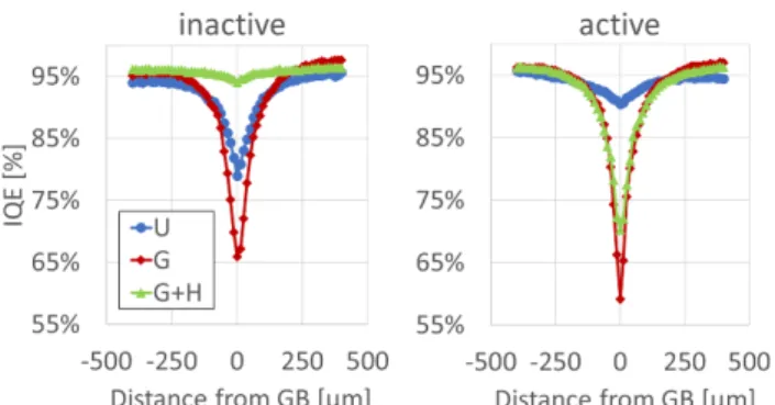
Like most grain boundaries in the material, the ‘inactive’ GB has its contrast, and thus recombination activity, increased during gettering. The contrast increases from 17% in the ungettered state to 32% after gettering. After hydrogenation it is reduced to very low levels, about 2%, having a relatively small effect on IQE. The activity of the ‘active’ grain boundary is also increased during gettering, but here the increase is stronger, from an IQE contrast of 5% to 39%. The main difference is that hydrogen passivation reduces the contrast only slightly, down to 27%. The GB is still visible on the map and acts as a recombination site, affecting the overall IQE of the device.
Figure 5 Sum of active and inactive GB segment lengths for each type and average IQE contrast of the active segments. Active
segments are defined as showing an IQE contrast equal to or above 5%. The arrows in the chart legend indicate the respective axis for each data set. The analysis was performed on an area of 375 mm2, of which part is visible in Figure 3.
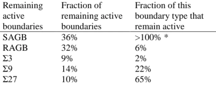
An overview of the active grain boundary length and the average IQE contrast of different grain boundary types is presented in Figure 5 and additional details can be found in Table 1. The classification is based on defining the active grain boundaries as having an IQE contrast at or above 5 %, and those with contrast below as well passivated and inactive. The average IQE contrast for a given grain boundary type is a weighted arithmetic mean of the contrast with active segment length of this type as weight. While many random-angle grain boundary segments are still recombination active, they are only a small fraction of all the RAGBs detected in the material and their activity, and thus the effect on cell performance is smaller than that of small-angle grain boundaries. Most of the active grain boundary segments show a similar IQE contrast, but the active Σ27 segments show higher contrast values, about 33%, which is twice the average contrast of RAGBs, and more than half of Σ27 grain boundaries remains active after full processing. Cases of Σ27 grain boundaries emitting dislocations have been presented in literature, and this can explain the higher recombination activity at boundaries of this type 25.
Additionally, more recombination active grain boundary segments were classified as SAGBs than were actually measured with EBSD. This is because the measurement system used in this study did not allow for precise detection of SAGB with misorientation angle below 5 °. When a recombination active boundary segment was found in the IQE maps, but could not be matched with a boundary measured by EBSD, it was classified as SAGB. An example of this is the dislocation cluster visible as an area with a higher density of recombination active grain boundaries near the right, upper corner of each IQE map in Figure 3. This dislocation cluster is “contained” within
6
a grain bounded by RAGB and CSL boundaries visible on the EBSD map, but no SAGB are detected within. Selective etching performed on these samples revealed a complex dislocation structure, consisting of a network of unindexed grain boundaries and etch pits from dislocations in their vicinity 8.
Table 1 Fraction of remaining active boundaries of each type in the total length of all active boundary segments, and fraction
of active boundaries for each type in the total length of grain boundaries measured with EBSD for this type. * - active GB segments visible on the IQE maps which were not found with EBSD were classified as SAGB, and thus more active SAGB were found on IQE maps than measured with EBSD.
Remaining active boundaries Fraction of remaining active boundaries Fraction of this boundary type that remain active SAGB 36% >100% * RAGB 32% 6% Σ3 9% 2% Σ9 14% 22% Σ27 10% 65%
As mentioned, special cases of CSL grain boundaries can also be found among the recombination active grain boundaries. The fraction of boundary type that remains active in Table 1 shows that for CSL grain boundaries the higher the coincidence index, the larger fraction of grain boundaries remain active, which is in agreement with other results reported in literature 5,7,26. These results are similar with the case for the bimodal contrast distribution
in the bottom of the ingot, and can be probably explained with difference in coherence of the grain boundaries. The recombination active segments, while some still being CSL, are macroscopically incoherent and induce stress in the lattice, in some cases probably relaxing it with dislocations. Such cases of recombination active grain boundaries with dislocations in their close vicinity were found when the samples have been selectively etched for dislocation cluster analysis 8. This macroscopic incoherence increases the number of available nucleation sites on
the grain boundary during gettering and a larger concentration of impurities is internally gettered on them. The precipitate distribution in their vicinity could potentially change during gettering so that more, but smaller precipitates are present. This would result in a larger precipitate surface, more difficult to passivate during hydrogenation.
Previous studies showed that Σ3 grain boundaries tend to be decorated with metals closer to the detection limit than other types of grain boundaries, but in this study Σ3 grain boundaries with high levels of recombination activity were found. To investigate the relation between the contamination level on such grain boundaries and their recombination activity, two Σ3 grain boundaries were selected from about 80 % ingot height. One inactive and one active Σ3 grain boundary before and after gettering were chosen to analyse their metal precipitate distribution by µ-XRF. The IQE maps of these grain boundaries, along with an EBSD map and the resulting µ-XRF maps can be seen in Figure 6. Table 2 contains the detection limits for the presented µ-XRF maps.
Table 2 Detection limits for each of the µ-XRF maps presented in Fig. 6. The values are given in ng/cm2.
µ-XRF map Fe Ni Cu
Inactive Ungettered 9 4 5 Inactive Gettered 9 4 5 Active Ungettered 8 3 4 Active Gettered 33 17 21
The grain boundary labeled as ‘Inactive’ showed no IQE contrast after each process step. The ‘Active’ grain boundary started showing strong IQE contrast after gettering and remained recombination active after hydrogenation. The measurement results can be seen in Figure 6. In the as-grown, ungettered material, large areas with high Fe, Ni, and Cu content were found near the inactive grain boundary. After gettering, no particles are present at the same grain boundary above the detection limit of the technique. An opposite situation occurred on the recombination active Σ3 grain boundary. No precipitates above the detection limit were found before gettering, but after the gettering process clusters of smaller metal precipitates are visible. Only a very limited number of four relatively small regions of interest could be analysed by µ-XRF in this study; however, the results indicate that contaminants are in the vicinity of this recombination-active grain boundary, suggesting a correlation.
7
Previous results showing that a change in Ni contamination levels on dislocation clusters was related to a change in their recombination strength 8 are in line with these results on grain boundaries. Strong signals from
iron, nickel and copper are found on the grain boundary that is activated during gettering. This grain boundary remains active after hydrogenation. If the active Σ3 grain boundary is macroscopically incoherent and contains dislocations in its structure, it results in a different nucleation site density. On coherent Σ3 GBs there are fewer nucleation sites and during gettering the dissolved impurities are extracted to the emitter. On the incoherent grain boundary, the increased nucleation site density leads to an internal gettering process, after which the recombination activity on the grain boundary increases.
3.3 Quasi-mono part of the ingot The material analysed in this study comes from a hybrid ingot
containing both HPMC and QM structure. The main focus is on the HPMC part, but the QM part was also analysed. The overall effect of grain boundaries on the IQE in the QM part was small due their nature and very low density. Small-angle grain boundaries were found in the QM part above the seed joint, their misorientation was measured to be below 5°. They showed an activity very similar to SAGB in the HPMC part, presented in section 3.2. Σ3 CSL grain boundaries could also be found in the QM part, but they showed no detectable recombination activity.
4. Conclusions
In this work, LBIC and EBSD measurements show that recombination activity of grain boundaries increases during gettering and is reduced in subsequent hydrogenation. About 90% of the random-angle grain boundaries are well passivated after standard cell processing. What remains recombination active are mostly small-angle grain boundaries, segments of random-angle grain boundaries, and special cases of CSL boundaries, on which a lack of coherence is suspected as a cause for increased nucleation site density.
The recombination activity in fully processed HPMC wafers is observed to be caused by dislocations in the form of clusters, SAGBs, and possibly as part of grain boundary structure reducing the macroscopic GB incoherence.
µ-XRF measurements of a typical inactive Σ3 grain boundary and a special case of this grain boundary type, activated during gettering, indicate that the change in recombination activity might be related to the presence of metals, as evidenced by a change in precipitate distribution on the extended defects.
Figure 6 EBSD and IQE of a sample area containing Σ3 grain boundaries, of which one is active and the other
inactive in the gettered and hydrogenated state (G+H), along with µ-XRF maps of areas in close vicinity to these grain boundaries in two process states: ungetered (U) and after gettering (G). The IQE maps in the U and G state roughly show the positions of where the µ-XRF analysis was performed with white squares A for the active, and I for the inactive Σ3 grain boundary. The µ-XRF maps are displayed in logarithmic scale (base 10), where the color-bars represent the exponent and the unit is ng/cm2.
8
Acknowledgements The work reported in this paper was performed in the project Impurity Control in High
Performance Multicrystalline Silicon, 228930/E20, funded by the Norwegian Research Council’s ENERGIX programme and industry partners REC Solar, REC Silicon, Steuler Solar and The Quartz Corp. Part of this work was also supported by the SOPHIA project "HPSS", the Solar-Era. Net project "HighCast" via the Swedish Energy Agency, and the project "Advanced analysis of industrial silicon wafers for solar cells" by J. Gust. Richert stiftelse, which is gratefully acknowledged. The authors would like to thank Tonio Buonassisi for his comments on this work. M. A. Jensen and E. E. Looney acknowledge support by the National Science Foundation (NSF) Graduate Research Fellowship under Grant No. 1122374, and the NSF and the US Department of Energy under NSF CA No. EEC-1041895. This research used resources of the Advanced Photon Source, a U. S. Department of Energy (DOE) Office of Science User Facility operated for the DOE Office of Science by Argonne National Laboratory under Contract No. DE-AC02-06CH11357.
References
1
ITRPV and VDMA, 8 ed. (ITRPV, VDMA Photovoltaik Equipment, Frankfurt, Germany, 2017).
2Fraunhofer Institute for Solar Energy Systems, “Photovoltaics Report,” (2017).
3
M. Rinio, A. Yodyungyong, S. Keipert-Colberg, D. Borchert, and A. Montesdeoca-Santana,
Phys. Status Solidi A 208, 760 (2011).
4
S. Castellanos, M. Kivambe, J. Hofstetter, M. Rinio, B. Lai, and T. Buonassisi, Journal of
Applied Physics 115 (2014).
5
J. Chen, T. Sekiguchi, D. Yang, F. Yin, K. Kido, and S. Tsurekawa, J. Appl. Phys. 96 (2004).
6M. Di Sabatino and G. Stokkan, physica status solidi (a) 210, 641 (2013).
7
T. Buonassisi, A. A. Istratov, M. D. Pickett, M. A. Marcus, T. F. Ciszek, and E. R. Weber, Applied
Physics Letters 89, 042102 (2006).
8
K. Adamczyk, R. Søndenå, C. C. You, G. Stokkan, J. Lindroos, M. Rinio, and M. Di Sabatino,
physica status solidi (a) (2017).
9
C. W. Lan, A. Lan, C. F. Yang, H. P. Hsu, M. Yang, A. Yu, B. Hsu, W. C. Hsu, and A. Yang, Journal
of Crystal Growth (2016).
10
C. W. Lan, W. C. Lan, T. F. Lee, A. Yu, Y. M. Yang, W. C. Hsu, B. Hsu, and A. Yang, Journal of
Crystal Growth 360, 68 (2012).
11
K. E. Ekstrøm, G. Stokkan, A. Autruffe, R. Søndenå, H. Dalaker, L. Arnberg, and M. Di Sabatino,
Journal of Crystal Growth 441, 95 (2016).
12
L. Priester, Grain Boundaries - From Theory to Engineering, Vol. 172 (Springer, 2013).
13N. Sakaguchi, M. Miyake, S. Watanabe, and H. Takahashi, Materials Transactions 52, 276
(2011).
14
F. Komninou, T. Karakostas, G. Bleris, and N. Economou, Journal de Physique Colloques 43, 9
(1982).
15
J. Chen and T. Sekiguchi, Japanese Journal of Applied Physics 46, 6489 (2007).
16
G. Stokkan, M. Di Sabatino, R. Søndenå, M. Juel, A. Autruffe, K. Adamczyk, H. V. Skarstad, K.
E. Ekstrøm, M. S. Wiig, C. C. You, H. Haug, and M. M‘Hamdi, physica status solidi (a) 214,
1700319 (2017).
17
M. Taguchi, A. Terakawa, E. Maruyama, and M. Tanaka, Progress in Photovoltaics: Research
and Applications 13, 481 (2005).
18
M. Rinio, H. J. Möller, and M. Werner, Solid State Phenomena 63-64, 115 (1998).
19
G. Palumbo, K. T. Aust, E. M. Lehockey, U. Erb, and P. Lin, Scripta Materialia 38, 1685 (1998).
20A. Autruffe, M. M'Hamdi, F. Schindler, F. D. Heinz, K. E. Ekstrøm, M. C. Schubert, M. Di
Sabatino, and G. Stokkan, Journal of Applied Physics 122, 135103 (2017).
21Z. Cai, B. Lai, W. Yun, I. McNulty, A. Khounsary, J. Maser, P. Ilinski, D. Legnini, E.
Trakhtenberg, S. Xu, B. Tieman, G. Wiemerslage, and E. Gluskin, in Performance of a
high-resolution x-ray microprobe at the Advanced Photon Source, Stanford, California, USA, 1999
(American Institute of Physics Conference Proceedings), p. 31.
22
S. Riepe, I. E. Reis, W. Kwapil, M. A. Falkenberg, J. Schön, H. Behnken, J. Bauer, D.
Kreßner-Kiel, W. Seifert, and W. Koch, physica status solidi (c) 8, 733 (2011).
9
23
D. Macdonald, A. Cuevas, A. Kinomura, Y. Nakano, and L. J. Geerligs, Journal of Applied
Physics 97 (2005).
24
J. Lu, M. Wagener, G. Rozgonyi, J. Rand, and R. Jonczyk, Journal of Applied Physics 94, 140
(2003).
25
A. Autruffe, V. S. Hagen, L. Arnberg, and M. Di Sabatino, Journal of Crystal Growth 411, 12
(2015).
26