Performance of MLSE over Fading Channels
Author:
Aftab Ahmad
Date: 2013-05-31
Subject: Electrical Engineering
Level: Master Level
teachers
1Brown, James Dean, and Theodore S. Rodgers. Doing Second Language Research: An introduction
to the theory and practice of second language research for graduate/Master’s students in TESOL and Applied Linguistics, and others. OUP Oxford, 2002.
This work examines the performance of a wireless transceiver system. The environment is indoor channel simulated by Rayleigh and Rician fading channels. The modulation scheme implemented is GMSK in the transmitter. In the receiver the Viterbi MLSE is implemented to cancel noise and interference due to the filtering and the channel. The BER against the SNR is analyzed in this thesis. The waterfall curves are compared for two data rates of 1 M bps and 2 Mbps over both the Rayleigh and Rician fading channels.
Abstract . . . 3 Acknowledgments . . . 4 List of Figures . . . 7 1 Introduction 8 1.1 Thesis Contribution . . . 9 1.2 Thesis Layout . . . 9
2 Digital Modulation Schemes 10 2.1 Introduction to GMSK . . . 10
2.2 GMSK Development:A Preface to GMSK . . . 10
2.2.1 Binary Phase Shift Keying: BPSK . . . 10
2.2.2 Quadrature Phase Shift Keying: QPSK. . . 13
2.2.3 Offset Quadrature Phase Shift Keying: OQPSK . . . 15
2.2.4 Minimum Shift Keying: MSK . . . 17
2.3 Gaussian Minimum Shift Keying:GMSK . . . 22
3 Transmitter Implemented in Matlab 25 3.1 Over sampler: . . . 25
3.2 Zero Order Hold(ZOH) . . . 26
3.3 Gaussian filter. . . 27
3.4 Analog front end . . . 28
4 Channels 30 4.1 Introduction . . . 30
4.2 AWGN Channel. . . 30
4.3 Fading Channels . . . 31
4.3.1 Large Scale Fading . . . 31
4.3.2 Small Scale Fading/Multi path fading. . . 32
4.3.3 Impulse Response Characterization . . . 33
4.4 One number Parameters for Multi paths . . . 34
4.5 Small Scale Fading Types . . . 36
4.5.1 Multi path fading due to Delay Spread . . . 36
4.5.2 Multi path fading due to Doppler Spread: BD . . . 36
4.6 Rayleigh Fading Distribution . . . 37
4.7 Rician Fading Distribution. . . 38
5 Receiver Implemented in Matlab 39 5.1 Receiver RF Front End. . . 39
5.2 The Digital Baseband Processing . . . 40
5.2.1 Synchronization . . . 40
5.2.2 Demodulation . . . 43
5.2.3 Demodulation . . . 44
5.2.4 Detection. . . 44
5.2.5 Maximum Likelihood Sequence Estimation(MLSE) Viterbi . . . 44
6 Simulation Results 46 6.1 Rayleigh Fading Channel. . . 46
1.1 the radio and micro waves band . . . 8
2.1 constellation diagram for BPSK . . . 11
2.2 BPSK Modulator . . . 11
2.3 NRZ pulse for BPSK . . . 12
2.4 PSD of BPSK . . . 12
2.5 constellation diagram for QPSK . . . 13
2.6 QPSK Modulator . . . 14
2.7 QPSK Waveform (simulated)with the phase transitions. . . 14
2.8 PSD of QPSK. . . 15
2.9 constellation diagram for QPSK . . . 16
2.10 constellation diagram for QPSK . . . 16
2.11 constellation diagram for OQPSK. . . 16
2.12 PSD of MSK OQPSK . . . 17
2.13 the phase trajectory taken by binary CPFSK . . . 18
2.14 the phase trellis, boldfaced path shows the bit sequence 1101000. . . 19
2.15 MSK constellation diagram . . . 21
2.16 Gaussian impulse response of filter for BT values of 0.25 and 0.5 . . . 23
2.17 PSD of GMSK and MSK. . . 23
2.18 PSD of GMSK and MSK. . . 24
2.19 response of filter to individual pulses . . . 24
3.1 oversampling rates: Nyquist rate and by a factor of 8. . . 26
3.2 Impulse response of the ZOH . . . 26
3.3 Impulse response of the ZOH . . . 27
3.4 absolute value of the Fourier transform of the impulse response of the ZOH . . . 27
3.5 sum of the responses of individual pulses . . . 28
3.6 the final gmsk modulated signal to be transmitted wirelessly. . . 29
3.7 GMSK modulation implemented in the transmitter . . . 29
4.1 model for received signal through AWGN channel . . . 30
4.2 path loss,shadowing and multi path effects on received power . . . 32
4.3 Shadowing . . . 32
4.4 Impulse Response model of the channel . . . 33
4.5 Impulse Response model of the channel . . . 34
4.6 Fading channels categorized . . . 37
5.1 The Receiver diagram:Analog Part . . . 40
5.2 The complete Digital Receiver diagram with the Frame synchronization . . . 43
5.3 Matched Filter Frequency Response. . . 43
5.4 The Receiver diagram:the Digital Demodulator Part . . . 45
5.5 A trellis diagram with a chosen path by the Viterbi algorithm . . . 45
6.1 BER vs. SNR over 4 multipaths through Rayleigh fading channel . . . 47
6.2 BER vs. SNR over 4 multipaths through Rayleigh fading channel . . . 47
6.3 BER vs. SNR over 4 multipaths through Rician fading channel . . . 48
6.4 BER vs. SNR over 4 multipaths through Rician fading channel . . . 48
The radio spectrum or the electromagnetic spectrum includes frequencies up until 300 GHz. It is divided into different bands in every country for different purposes. The waves are classified under different bands of frequencies. The waves are referred to as radio waves,microwaves, infrared waves, light waves, ultra violet rays, x-rays, and gamma rays depending on which band they are in. Each band is further divided into smaller bands.The radio band is of our interest,the range of frequencies of which can be seen in the figure1.1[1].
Figure 1.1: the radio and micro waves band
The industrial, scientific, and medical (ISM) band as it is called is the band of frequencies which are employed in applications in the aforementioned fields. The federal communications committee (FCC) allowed 3 ISM bands for unlicensed users in the field of communications. The bands can be seen in the table1.1[2].
In the ISM band are the waves of frequencies falling in the radio band range that carry energy radiated by applications like microwave ovens and diathermy machines to name some. This band allows alongside applications in the three fields mentioned earlier unlicensed applications in the field of communications. Some communications applications are wireless local area networks LAN s, Blue tooth protocol, Zig bee, Personal area networks, Wifi, IEEE 802,15,4, IEEE 802,11, radio frequency identification applica-tions(RFID) like biometric passports readers and near field communication applications.These are all
Table 1.1: Frequency bands allotted by FCC
Name of band
frequency bandwidth for each band
part 15.247
ISM band
902-928 MHz(26 MHz)
2400-2483.5 MHz(83.5MHz)
5725-2850 MHz(125MHz)
part 15 subpart E
U-NII band
5150-5250 MHz(100 MHz)
5250-5350 MHz(100MHz)
5725-5825 MHz(100MHz)
part 15 subpart D
U-PCS band
1910-1920 MHz(10 MHz)
2390-2400 MHz(10MHz)
1920-1930 MHz(10MHz)
part 15.255
59-64 GHz
unlicensed applications working at 915 MHz, 2.450 GHz, or 5.800 GHz.For being unlicensed they must be able to cope with electromagnetic interference from other non-communication devices but in return can not cause any interference to other ISM users. The devises operating according to any of the proto-cols mentioned are referred to as users.This constraint is set by the FCC. As one can predict this leads them to be very low power devices i.e,. maximum 1 Watt (30 dB m).Along with power there is also the frequency domain constraint to satisfy in presence of nearby frequency band users.
1.1
Thesis Contribution
The work in this thesis is a study and performance of a wireless transceiver system operating on 2.4 GHz. Referring to table 1.1we see 2.4 GHz is in the ISM band. A transceiver is a communication device that houses both the transmitter and a receiver and mostly the circuitry is common to some extent for both parts. This frequency is in the ISM band hence the transceiver is to operate at low power and share with other unlicensed users like wifi, blue tooth etcetera. The objective is to see the performance of this transceiver via the bit error rate (BER) against signal to noise ratio (SNR) curves. The idea is to simulate an indoor channel so as to simulate the situation of a consumer electronics device like a television interacting with a hearing aid device.The room environment is simulated with an indoor channel. The digital data bits transmit through this channel and through all the filters in the transmitter and receiver are bound to be different due to noise in digitization,modulation,channel, and filters. In the receiver we implement a mitigating technique to reduce the errors that the channel and the filters will have induced into the transmitted data sequence wise. The technique is called maximum likelihood sequence estimation (MLSE) which is implemented by the Viterbi decoding method.
1.2
Thesis Layout
The division of this thesis is given as follows. Chapter 1 is an introduction to this thesis and gives an overview of the whole thesis. Chapter 2 discusses the background needed to gradually realize the GMSK scheme which is central to the transmitter of this thesis.Chapter 3 discusses the major blocks that simulate the transmitter in matlab. Chapter4discusses the channel that the data encounters in the air. Chapter5 discusses the receiver simulated in matlab. Chapter 6 shows the simulation results and chapter7gives concluding remarks and suggestions for future work.
2.1
Introduction to GMSK
The frequency of operation of the transceiver is the 2.4 GHz frequency range which is very crowded as the spectrum is shared with other communication protocols such as blue tooth. So this transceiver must operate in this crowded environment while not allowing noise, i.e,inter symbol and inter channel interference to undermine its performance. This fact and low power constraint will dictate the choice of the modulation scheme that is implemented.Normally the power radiated out side the band should be 60-80 dB fewer than the power radiated in the adjacent band [3]. To fulfill this the power spectrum has to be engineered but not at the RF stage as there the frequency can vary. The spectrum is manipulated either in the baseband or in intermediate frequency band and then up sampled and modulated and passed through power amplifiers.
In light of the above discussion a narrow-band digital modulation scheme with constant envelope called the Gaussian Minimum Shift Keying GMSK is used in the transceiver. A constant envelope is desired. The reason is that if raw data bits with some data encoding like non return to zero (NRZ) are directly frequency modulated they would be spread over an infinite band in the frequency domain. If some low pass filtering is applied the result would be that in time domain the sharp transitions of data bits will be smoothed and a compact spectrum would be under utilization [4]. In the next section a stepwise development of simpler modulation schemes is presented in arriving at the description of GMSK.
2.2
GMSK Development:A Preface to GMSK
2.2.1
Binary Phase Shift Keying: BPSK
In BPSK the binary information is in the two phase shifts of the carrier corresponding to a binary 0 or a 1 , basically the carrier signal takes two amplitude levels. The symbols for both the amplitude levels can be generalized as Si(t) = p (2Eb/Tb)cos(2πfct + (i − 1)π), 0 ≤ t ≤ Tb i = 1, 2 fc= 1/Tb, (2.1)
where Eb is the bit energy, Tb is the bit duration and fc is the carrier frequency. If fc is an integer
multiple of 1/Tb phase transitions will occur at the same points of the carrier signal. In equation 2.1
the individual signals of the BPSK scheme are S1(t) = −S2(t).The normalized basis function for BPSK
signals is given by
φ(t) =p2/Tbcos(2πfct). (2.2)
The vector coefficients for the BPSK signal are given by S11= Z Tb 0 S1(t)φ(t) dt. = p Eb and S21= Z Tb 0 S2(t)φ(t) dt. = − p Eb.
S1(t) is represented by the amplitude
√
Eb while S2(t) is represented by the amplitude −
√
Eb. The
symbols that represent S1(t) and S2(t) can be visualized on a constellation diagram in the figure 2.1
[5,6]. A 0 can be represented by −√Eb and a 1 can be represented by
√ Eb.
Figure 2.1: constellation diagram for BPSK
The two symbols are farthest away from each other on the constellation diagram. This has the advantage that it would take a lot of noise to corrupt one symbol to be interpreted as the other at the demodulator. The disadvantage is that only one bit is encoded onto one symbol.
BPSK Modulator
As already stated A 0 can be represented by −√Eb and a 1 can be represented by
√
Eb. This is NRZ
encoding of the data bits as shown in figure 2.3. These bits when multiplied with the basis function for BPSK generate the BPSK signal as expressed mathematically in 2.1. A BPSK modulator can be visualized as in figure2.2[7]
Figure 2.2: BPSK Modulator
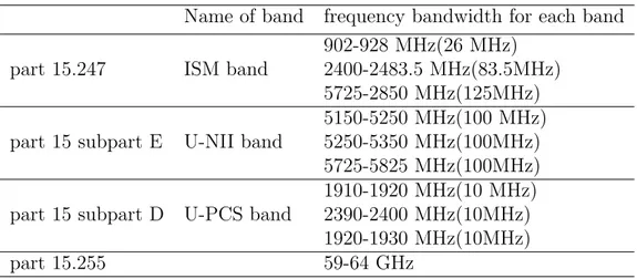
Power Spectral Density (PSD) of BPSK signal
The BPSK signal can be referred to as a bipolar non return to zero (NRZ) random signal that consist of rectangular pulses. Both 0 and 1 are represented by essentially the same pulse of opposite polarity,any of the two bits is equally likely in the stream of bits.The rectangular pulse is let’s say g(t) with duration Tb and magnitude ±p2Eb/Tb. It is shown in the figure2.3.
Figure 2.3: NRZ pulse for BPSK
The PSD of the rectangular pulse is given as in figure2.3and mathematicallly as[5]. SB(f ) = (2Eb/Tb)(Tb2sinc
2(f T
b)/Tb) = 2Ebsinc2(f Tb). (2.3)
The PSD of the BPSK signal is
S(f ) = (1/4)[SB(f − fc) + SB(f + fc)], (2.4)
or
S(f ) = (Eb/2)sinc2[(f − fc)Tb] + (Eb/2)sinc2[(f + fc)Tb]. (2.5)
The PSD of the BPSK signal is shown in the figure2.4
Figure 2.4: PSD of BPSK
In BPSK modulation case minimum occupied bandwidth B equals the bit rate Rb. The spectral
efficiency for BPSK case is 1bit/s/Hz. The spectral efficiency measures how much data a modulation scheme can pack which is by definition the ratio of the transmitted bit rate and the occupied bandwidth and given in equation2.8as
ρ = Rb/B. (2.6)
The bit rate and the bit period are reciprocally related, so
Rb= 1/Tb. (2.7)
Hence
ρ = Rb/(1/Tb) = 1bit/s/Hz. (2.8)
The bit error probability of BPSK modulated signal is given by Pe,BP SK= Q(
√
2Eb/No).[13] (2.9)
2.2.2
Quadrature Phase Shift Keying: QPSK
QPSK is a higher order modulation scheme. It uses four symbols for encoding;two bits encoded into one symbol. So more data can now be encoded. The four QPSK symbols can be generally mathematically represented as
Si(t) =
(p
(2Es/Ts)cos(2πfct + (2i − 1)π/4), 0 ≤ t ≤ Ts
0, otherwise, (2.10)
where i =1,2,3,4. Esis energy of transmitted symbol,symbol duration is denoted by Tsand fc is the
carrier frequency.
Equation2.10can be written as
SQP SK(t) = (2Es/Ts)cos(2πfct)cos[(2i − 1)π/2] − (2Es/Ts)sin(2πfct)sin[(2i − 1)π/2], (2.11)
the basis functions for QPSK are φ1(t) =p(2/Ts)cos(2πfct) and φ2(t) =p(2/Ts)sin(2πfct) . In terms
of the basis functions equation2.12can be written as
SQP SK(t) = Escos[(2i − 1)π/4]φ1(t) − Escos[(2i − 1)π/4]φ2(t), i = 1, 2, 3, 4. (2.12)
The symbols that represent the four possible phases can be visualized on the constellation diagram.
Figure 2.5: constellation diagram for QPSK
QPSK Modulator
The QPSK modulator was mathematically shown in equation equation2.12and a block diagram is shown in figure2.6[7,8,9].
Figure 2.6: QPSK Modulator
The input bit stream is converted into an even and an odd bit stream by the serial to parallel converter. The bits are then converted according to the NRZ scheme.Just like the BPSK case we assign a −√Eb to 0 and a
√
Eb to 1. Just like the BPSK case the NRZ symbols are multiplied with the basis
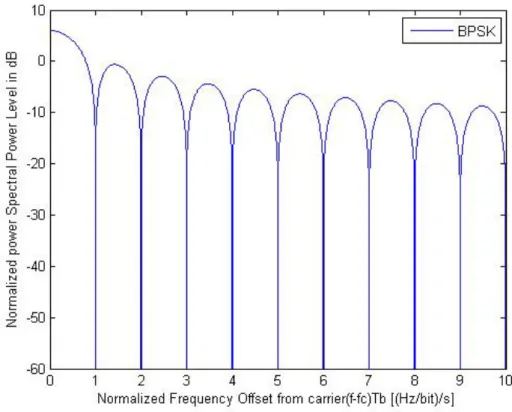
functions but afterwards are added to form the QPSK symbols. The QPSK waveform as an addition of two BPSK waveforms(from the even and odd bit stream) is shown in figure and2.7.
Figure 2.7: QPSK Waveform (simulated)with the phase transitions
Each symbol comprising of two bits dictates that symbol energy Es = 2Eb and on the
constel-lation diagram each adjacent symbol is √2Es.In terms of bit energy the adjacent symbols are 2
√ Eb
[7].Depending on if one or both bits change after a particular symbol the phase can change by 90◦
degrees or 180◦ degrees respectively for the next symbol. We discuss one case to illustrate the abrupt phase transitions.If we concentrate on the first pair of bits in the original incoming bit stream they are separated and become the first bits of both the even and odd bit streams.The second pair of bits in the original bit stream are separated and become the second bits of the even and odd bit streams.Each bit in the odd and even bit stream has a bit duration twice as that in the original bit stream.The first odd bit and the first even bit add to give the first QPSK symbol and this continues.Since there are two bits employed in forming a QPSK symbol the symbol rate is half that of the bit rate. In QPSK the carrier phase changes sign after every two bit periods due to the symbol spread over two bits.The first pair of (odd,even) bits is (0,1). The second is (1,0).So in transition from one QPSK symbol to the next both the constituent BPSK symbols have changed. This causes a phase transition of 180◦degrees and is shown as an abrupt change in the QPSK waveform phase. If only one BPSK symbol had changed in the transition the phase transition of 90◦ degree would occur. This explanation of phase transitions of 90◦ degree and 180◦degree is evident in the constellation diagram2.11.The line through the origin indicates a 180◦ degree phase shift while the remaining lines indicate a 90◦ degree phase shift between successive
symbols.These sudden shifts of phase will have the effect that the spectrum will expand. To limit the spectrum we can filter the modulated data.That will have the undesired effect that we may not have the constant envelope.At the symbol transition where both bits change the envelope may go to zero for an instant.
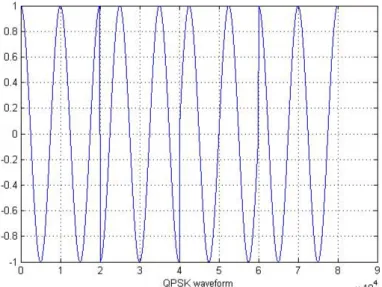
Power Spectral Density PSD and Probability of bit errorP
eof QPSK signal
The PSD of QPSK is given as
PQP SK = Es/2[(sinπ(f − fc)Ts/π(f − fc)Ts)2+ (sinπ(−f − fc)Ts/π(−f − fc)Ts)2], (2.13)
where Tsis the symbol period.In terms of the bit period Tbequation 2.13can be written as
PQP SK= Eb[(sin2π(f − fc)Tb/2π(f − fc)Tb)2+ (sin2π(−f − fc)Tb/2π(−f − fc)Tb)2]. (2.14)
The PSD of QPSK is shown in the figure2.8[7]
Figure 2.8: PSD of QPSK
and the bit error probability of QPSK in an additive white Gaussian noise (AWGN) channel is Pe,QP SK = Q(
√
2Eb/No). (2.15)
The bit error probability for QPSK is the same as BPSK. But twice as much data is sent using QPSK as compared to BPSK according to the relation2.6and2.8but here the bandwidth of the signal is half the data rate(one bit is spread over two periods).So equation2.8becomes
ρ = Rb/(1/2Tb) = 2bit/s/Hz. (2.16)
2.2.3
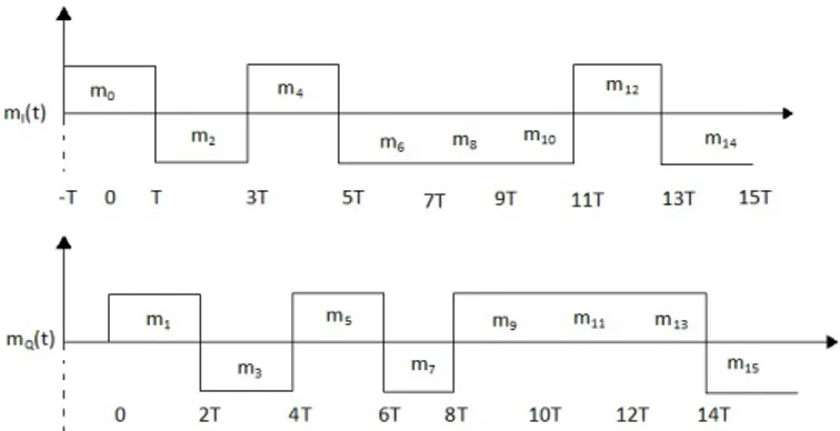
Offset Quadrature Phase Shift Keying: OQPSK
OQPSK is similar to QPSK. In QPSK there were two rectangular bit streams amplitude modulated on a cosinus and a sinus wave that both changed after two bit periods. In OQPSK one bit stream is simply delayed by one bit interval initially2.9.
Figure 2.9: constellation diagram for QPSK
The bit period is still two. Due to the initial one bit shift of the quadrature bit stream the bits will never change value or the phase will never change phase at the same time. Due to this innovation we have eliminated the phase changes between successive symbols to only 90◦ degrees and they can occur at every bit i.e., one bit in one bit stream has completely passed while a bit in the other stream is in the process.OQPSK was designed so that after filtering the spectrum to make it compact the envelope may stoop towards 0 at the 90◦ degrees phase change but will not completely go to zero as in the QPSK case. The constellation diagram for OQPSK is shown.We can compare the difference with QPSK .
Figure 2.10: constellation diagram for QPSK
Figure 2.11: constellation diagram for OQPSK
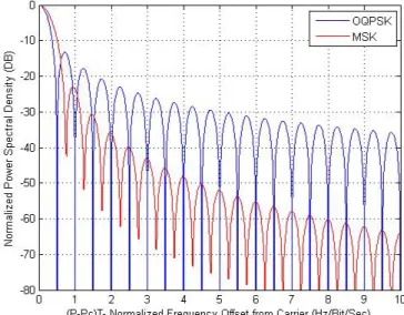
The PSD of OQPSK is identical to that of QPSK [7].The PSD of OQPSK and MSK is shown in figure
2.12[11]. MSK is discussed in the next coming section.By looking at2.12one notices the width of the main lobe of the MSK spectrum is 1.5 times wider than that of OQPSK and its sidebands decay to below -60 dB. In our case the wide main band of MSK is not attractive. To cope with this we will discuss GMSK in later sections.
Figure 2.12: PSD of MSK OQPSK
2.2.4
Minimum Shift Keying: MSK
QPSK has abrupt changes of 90◦ degree and 180◦ degree in its waveform as seen in 2.7. OQPSK has 90◦ degree abrupt jumps in its waveforms.These abrupt changes in the time domain have disastrous effects in the frequency domain.The baseband spectrum becomes wide and high frequency components arise [8,9,10,12].These high frequency components have to be filtered by low pass filters. These filters along with suppressing side lobes cause inter symbol interference. QPSK and OQPSK modulated signals have constant amplitudes but QPSK exhibits phase changes at the symbol rate while OQPSK exhibits phase changes the bit rate. The phase changes occur because the data or the information is in these phase changes.On filtering these signals they undergo amplitude variations at the phase change instants violating the constant amplitude characteristic of these modulated signals [7].
To cope with these problems is a modulation scheme called minimum shift keying (MSK) which has properties distinguishing it from QPSK. The MSK waveform is smoother than either QPSK and QPSK, there are no abrupt jumps in the phase of MSK such as those in QPSK seen in 2.7. The main lobe of the PSD of MSK is 1.5 times wider than that of QPSK as proved in2.12.
MSK is a Continuous Phase Modulation(CPM) scheme, a special form of binary continuous phase frequency shift keying (CPFSK)[13, 14].Consider a continuous phase frequency shift keying (CPFSK) signal, which is defined for the interval 0 ≤ t ≤ T b2.17
S(t) = (p
2Eb/Tbcos[2πf1t + θ(0)], f or symbol 1
p2Eb/Tbcos[2πf2t + θ(0)], f or symbol 0,
(2.17)
where Eb is the transmitted signal energy per bit, and Eb is the bit duration. The phase θ(0),
denoting the value of the phase at time t=0, sum up the past history of the modulation process up to time t=0. The frequencies f1 and f2 are sent in response to binary symbols 1 and 0 appearing at the
modulator input, respectively. Another useful way of representing the CPFSK signal S(t) is to express it in the conventional from of an angle modulated signal as [13]
S(t) =p2Eb/Tbcos[2πfct + θ(t)], (2.18)
where θ(t) is the phase of S(t). Where the phase θ(t) is a continuous function of time, we find that the modulated signal S(t) itself is also continuous at all times, including the inter bit switching times. The phase θ(t) of a CPFSK signal increases or decreases linearly with time during each bit duration of Tb
seconds, as shown by
fc− h/2Tb = f2. (2.21)
The information is frequency modulated on the carrier in the form of these discrete frequencies.We can solve for fc and h and get the relations
fc= 1/2(f1+ f2) (2.22)
and
h = Tb(f1− f2). (2.23)
To clarify the phase continuity of the MSK signal a term phase trellis is introduced.
Phase Trellis
CPFSK is a special case of CPM.As the name suggests this is a digital modulation scheme with the condition that the phase of the signal is continuous. This continuity dictates memory in the frequency modulator. The digital bits transmission via frequency shift keying (FSK) is done so by discrete shifts in the carrier of the signal.If we look at equation2.28we see that at time t = Tb
θ(Tb) − θ(0) =
(
πh, f or symbol 1
−πh, f or symbol 0. (2.24)
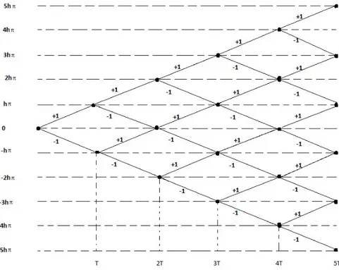
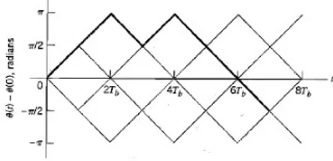
So the phase of the CPFSK signal2.17increases or decreases by ±πh straight lines; the slope of these straight lines are the frequency changes. Figure2.13which is a phase tree clarifies the phase trajectory across boundary intervals of the incoming data bits.
The phase of this CPFSK signal is an odd multiple of ±πh radians at odd multiples of bit duration Tb and likewise is an even multiple of ±πh radians at even multiples of bit duration. If the deviation
ratio h = 1/2 the phase can take on values of only ±π/2 at odd multiples of Tb and 0 and π at even
multiples of Tb. This info can be verified for the generalized h and an h=1/2 in the figures2.13and2.14
respectively.Figure2.14is shown for a specified bit sequence of 1101000 with θ(0)=0 [9].
Figure 2.14: the phase trellis, boldfaced path shows the bit sequence 1101000
By virtue of setting the modulation index h = 1/2 in2.23MSK is attained. The modulated carrier signal is [13]
S(t) =p2Eb/Tbcos[2π(fc+ In/4T )t − nπIn/2 + θ(n)], nT ≤ t ≤ (n + 1)T, (2.25)
where In is a sequence of M-ary information symbols from the alphabet ±1, ±3, .... ± (M − 1).Basing on
the value of In in the interval nT ≤ t ≤ (n + 1)T which can take on values ±1 for the binary CPFSK the
equation2.25can be expressed as a sinusoid having two possible frequencies defined as f1 = fc− 1/4T
f2= fc+ 1/4T . Equation2.25can be generalized as
Si(t) =
p
2Eb/Tbcos[2πfit + θ(n) + 1/2πn(−1)i− 1], i = 1, 2, (2.26)
.As iterated earlier information is frequency modulated on the carrier in the form of discrete frequency shifts. f2− f1= 1/2T is the minimum necessary frequency separation for the orthogonality of the signals
over a signal interval T . Hence CPFSK with h = 1/2 is called MSK. The phase in the nth signaling interval is a result of a phase continuing from previous adjacent symbols.
Signal Space Diagram of MSK
Equation2.18can express CPFSK signal in terms of [13] S(t) =p2Eb/Tbcos[(θ(t))]cos(2πfct) −
p
2Eb/Tbsin[θ(t)]sin(2πfct). (2.27)
We focus on the inphase componentp2Eb/Tbcos[θ(t)] with h = 1/2 we have from equation2.28
θ(t) = θ(0) ± (π/2Tb), 0 ≤ t ≤ Tb, (2.28)
where the plus sign corresponds to symbol 1 and the minus sign corresponds to symbol 0. A similar result holds for θ(t) in the interval −Tb ≤ t ≤ 0, except that the algebraic sign is not necessarily the
same in both intervals. Since the phase θ(0) is 0 or π, depending on the past history of the modulation process, we find that, in the interval −Tb ≤ t ≤ Tb , the polarity of cos[θ(t)] depends only on θ(0),
regardless of the sequence of 1’s and 0’s transmitted before or after t=0. Thus, for this time interval, the inphase component SI(t) consists of a half cycle cosine pulse defined as .
(2.29) SI(t) = p 2Eb/Tbcos[θ(t)] =p2Eb/Tbcos[(θ(0))]cos(πt/2Tb) = ±p2Eb/Tbcos(πt/2Tb) , −Tb ≤ t≤ Tb,
where the plus sign corresponds to θ(0) = 0 and the minus sign corresponds to θ(0) = π. Similarly in the interval 0 ≤ t ≤ 2Tb the quadrature component of equation2.27consists of half cycle sine pulse,
where the plus sign corresponds to θ(Tb) = π/2 and the minus sign corresponds to θ(Tb) = −π/2. From
the previous discussion phase states θ(0) and θ(Tb) can each assume one of two possible values, any one
of the four possibilities can arise, as described in [9].
1. The phase θ(0) = 0 and θ(Tb) = π/2 correspond symbol 1 transmitted.
2. The phase θ(0) = π and θ(Tb) = π/2 correspond symbol 0 transmitted.
3. The phase θ(0) = π and θ(Tb) = −π/2 correspond symbol 1 transmitted.
4. The phase θ(0) = 0 and θ(Tb) = −π/2 correspond symbol 0 transmitted.
This implies that the MSK signal will assume any of four possible forms, depending on the values of θ(0) and θ(Tb). From equation2.27we deduce the basis functions φ1(t) and φ2(t) for MSK as:
φ1(t) = p 2/Tbcos(2πfct)cos(πt/2Tb), 0 ≤ t ≤ Tb, (2.31) φ2(t) = p 2/Tbsin(2πfct)sin(πt/2Tb), 0 ≤ t ≤ Tb. (2.32)
MSK signal can now be expressed in the form
S(t) = s1φ1(t) + s2φ2(t), −Tb≤ t ≤ Tb, (2.33)
where the coefficients s1 and s2 are related to the phase states θ(0) and θ(Tb), respectively.To evaluate
s1, we integrate the product S(t)φ1(t) between the limits −Tb and Tb as
(2.34) s1= Z Tb −Tb S(t)φ1(t) dx =pEbcos[θ(0)], −Tb≤ t ≤ Tb.
To evaluate s2, we integrate the product S(t)φ2(t) between the limits −Tb and Tb as
(2.35) s2= Z Tb 0 S(t)φ2(t) dx = −pEbcos[θ(Tb)], 0 ≤ t ≤ Tb. In equations2.34and 2.35
1. Both the integrals are evaluated for two bit periods
2. Upper and lower limits of the integration for s1 are shifted a bit period with respect to those for
s2.
3. 0 ≤ t ≤ Tb is the time interval in which both the phase states θ(0) and θ(Tb) are defined.
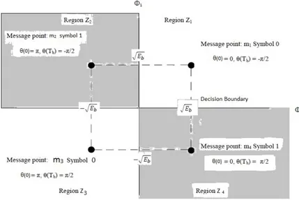
The signal constellation for an MSK signal is two dimensional, with four possible message points, as shown in the Figure2.15. The coordinates of the message points are (√Eb,
√ Eb),(− √ Eb, √ Eb),(− √ Eb, − √ Eb), and (√Eb, − √
Eb). The possible values of the phases of the inphase and quadrature components θ(0)
and θ(Tb) are also included in the figure2.15. The MSK and QPSK constellation diagrams are similar in
that both of them have four message points but there is a subtle difference.In QPSK each message point represents a symbol while in MSK two message points can represent symbol 0 and two message points
Transmitted Binary Symbols Phase States (radians) Coordinates of Message Points 0 ≤ t ≤ Tb θ(0) θ(Tb) s1 s2 0 0 −π/2 √Eb √ Eb 1 π −π/2 −√Eb √ Eb 0 π π/2 −√Eb − √ Eb 1 0 π/2 √Eb − √ Eb
Table 2.1: MSK signal space characteristics
can represent 1 at any particular time. Table2.1summarizes the value of the phases θ(0) and θ(Tb) as
well as corresponding values of s1 and s2 calculated for time intervals −Tb ≤ t ≤ Tb and 0 ≤ t ≤ 2Tb
respectively.The first column of the table indicates whether symbol 1 or symbol 0 was sent in the interval 0 ≤ t ≤ 2Tb.The coordinates of the message points, s1and s2, have opposite signs when symbol 1 is sent
in this interval, but the same sign when the symbol 0 is sent. For a given sequence of bits we can use the entries in the table2.1to derive the sequence of coefficients on a bit by bit basis to scale φ1(t) and
φ2(t) and hence determine the MSK signal S(t).
Figure 2.15: MSK constellation diagram
P
eand PSD:
The Pe for MSK is the same as that for BPSK and QPSK, so
Pe= Q(
√
2Eb/No). (2.36)
The PSD of MSK is obtained from taking the square of the magnitude of the Fourier transform of baseband pulse shaping function is given as in
P (t) = (
cos(πt/2Tb), t ≤ |Tb|
MSK was superior to QPSK and OQPSK in the time domain because it was a true continuous phase modulation scheme.The continuous phase and constant envelope are the features desirable because the idea was to keep low power consumption and narrow bandwidth utilization.The time domain property due to which MSK was arrived at is clear. The reason we did not employ MSK as our choice of the modulation scheme was that it’s spectrum is not compact enough. It’s main lobe is wider than that of OQPSK by 50 % as seen in figure2.12even though it’s side lobes are smaller. This is where the need for GMSK arose. MSK itself can be implemented by directly giving as input to a frequency modulator with a modulation index of 0.5. To make the spectrum slimmer or to reduce the energy in the upper side lobes of MSK all that is needed is to low pass filter the data stream before presenting it as input to the frequency modulator.This filter is a premodulation low pass filter referred to as a baseband pulse-shaping filter. The impulse response must have the following properties
1. Narrow bandwidth frequency response and sharp cutoff characteristics 2. Low overshoot impulse response
3. As in MSK the phase of the carrier of the modulated signal takes values ±π/2 at odd multiples of Tb and at even multiples of Tb it takes on values of 0 and π
The first property makes the wide MSK spectrum compact suppressing the high frequency compo-nents. Care is taken so as not to disturb the constant envelope of the waveform. The second property ensures that frequency deviations of the frequency modulated signal do not exceed their their limit. The third property ensures detection of the modulated frequency modulated signal. NRZ binary data stream when passed through this baseband pulse shaping filter whose impulse response is a Gaussian function. The frequency response of a Gaussian function is also Gaussian. The data is Gaussian filtered MSK modulated or GMSK modulated. The GMSK impulse response is given
h(t) =p2π/log2W exp((−2π2/log2)W2t2) (2.39) as in [9]. The response of this Gaussian filter to a rectangular pulse of unit amplitude and bit duration Tb is given by (2.40) f (t) = Z Tb/2 −Tb/2 h(t − τ )) dτ =p2π/log2W Z Tb/2 −Tb/2 exp((−2π2/log2)W2Tb(t − τ )2) dτ,
where W is the 3 dB bandwidth of the Gaussian filter. Equation2.40can be expressed as the difference of two complementary error functions as
f (t) = (1/2)[erf c(πp(2/log2)W Tb(t/Tb− 1/2)) − erf c(π
p
(2/log2)W Tb(t/Tb+ 1/2)). (2.41)
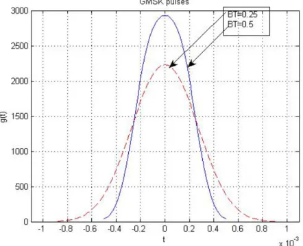
Figure 2.16: Gaussian impulse response of filter for BT values of 0.25 and 0.5
In erquation2.41the time bandwidth product W Tbis a design parameter. We note that as the W Tb
product decreases the pulse is spread in time and vice versa.The PSD of GMSK is compared wiht that of MSK and then with QPSK and BPSK in2.17and2.18.
Figure 2.18: PSD of GMSK and MSK
Due to it’s narrow bandwidth it is superior to MSK and the other modulation schemes in our application.It also has drawbacks. When a stream of NRZ data bits is passed through the GMSK filter the data is spread over onto the adjacent bits,inter symbol interference(ISI) is generated. The lower the W Tbproduct the farther out the tails of the Gaussian impulse response of the filter causes the modulating
signal to spread out.The choice of W Tb offers a trafeoff between compact spectrum and ISI[9].
Figure 2.19: response of filter to individual pulses
3
Transmitter Implemented in Matlab
We proceed to elaborate on the whole transmitter that fulfills our requirements of low power con-sumption via constant envelope modulation technique and narrow spectrum occupation.The major blocks implemented in Matlab are first listed and explained.
1. Incoming data:
The data from the mac layer enters the transmitter at two data rates of 1 and 2 M bps depending on the mode.
3.1
Over sampler:
Up sampling is the first and easiest choice when reconstructing a signal from it’s samples or the opposite. We up sample the incoming data at rates of 1 and 2 M bps by an oversampling rate (OSR) of 8. Up sampling a signal by a frequency at least twice as much as the highest frequency in the signal according to Nyquist criterion is absolutely necessary for reconstructing a signal from it’s samples but in practical applications not sufficient. In practice it is up sampled by a higher factor. Oversampling is useful in coping with aliasing as will be shown. Mathematically up sampling operation can be represented as
h(k) = (
g(k/L), if (k/L) is an integer.
0, otherwise. (3.1)
In actuality the up sampler inserts L − 1 zeros in between the sample values entering into it, where L is the up sampling factor. Higher up sampling is used so as to leave room for the transition gap between the spectral replicas so that a low pass filter can recover the continuous signal from it’s samples. To illustrate,equation3.1assumes that a signal is sampled according to the Nyquist rate so the spectral replicas won’t have any gap in between them.To recover the continuous time signal g(t) from the samples g(t) we would need an ideal low pass filter.
Figure 3.1: oversampling rates: Nyquist rate and by a factor of 8.
This isn’t possible. An infinite time delay in the response of filter could approximate the spectrum G(ω) of the samples g(t) but that is impractical. The transition band is non existent and to solve this exact problem is why we oversampled by a factor of 8 which is evident in the figure3.1.This provides ample space between spectral replicates of G(ω) which has the spectrum of G(ω) repeated at integral multiples of the sampling frequency. To recover G(ω) is easy now by low pass filtering as there is space for the transition band in which the spectrum sample can decay considerably before the next replica starts.Choosing a high enough data rate relaxes the strict requirement on the cutoff frequency of the filter. Our signals, without any shape filtering, are finite time bits with bit time period T b = 1/R where R is the rate of the data which is 1 and 2 M bps. Time limited signals have infinite band spectra.The spectrum G(ω) of samples g(t) will overlap no matter how high an OSR we oversample with.G(ω) due to overlapping tails of the copies of spectrum of G(ω) won’t contain a pure G(ω) and no amount of filtering won’t be able to retract G(ω) or g(t) but only a distorted version which will resemble G(ω) closely if the up sampling factor is chosen high enough. The reason for this aliasing is the spectral folding of tail of G(ω) beyond |f |> f s/2 [16]. In practice we use a cutoff filter which attenuates the spectrum beyond the f s/2 frequency. The zero order hold does this partially discussed next.
3.2
Zero Order Hold(ZOH)
The zero order hold block is essentially a reconstruction filter. The ultimate objective on the transmitter side is to shape digital pulses into continuous time and band limited train of symbols and then to frequency modulate them on a high frequency carrier to transmit them through a wireless channel.We give a brief description of the ZOH. The ZOH has a rectangular shaped impulse response h(t) = rect(t/T s) of amplitude 1 that we will refer to as a gate pulse as shown in figure3.2.
Figure 3.2: Impulse response of the ZOH
The digital data entering the zero order hold is essentially samples which we denote by f0(t).When these gate pulses pass through the reconstruction filter h(t) a continuous signal should be produced but as we will see the result will be only an approximation of a continuous signal. Let’s say the jth impulse of f0(t) has magnitude f (jT s) at t = jT s in time. It can be written as f (jT s)δ(t − jT s).This jth impulse will produce a gate pulse f (jT s)rect(t/T s) of strength f (jT s) centered at
t = jT s when it passes through the ZOH. Every sample will generate a gate pule proportional to it’s magnitude and give an output. the result is mathematically expressed as
x(t) =X
j=1
f (jT s)rect(t/T s) (3.2)
and is shown in the figure3.3[16]
Figure 3.3: Impulse response of the ZOH
We see it to be a staircase approximation of x(t). It isn’t smooth.The Fourier transform of the impulse response of the ZOH is denoted byF (Ω).We use the Nyquist rate T s = 1/2B,
f (t) = rect(t/T s) = rect(2Bt), (3.3)
F (Ω) = T sSinc(ωT s/2) = (1/2B)sinc(ω/4B) (3.4) The absolute value of the Fourier transform of the impulse response of the ZOH |F (Ω)| is shown in figure3.4.
Figure 3.4: absolute value of the Fourier transform of the impulse response of the ZOH
The effect that this ZOH has in time domain is a crude form of continuity even though it is only staircase and in the frequency domain the attenuation of the higher frequency components.
3.3
Gaussian filter
GMSK was proposed in this system study.It is the central point of discussion in the transmitter side of this transceiver.It is implemented by this Gaussian filter.This Gaussian impulse response filter provides all the desired properties of waveform and spectrum of GMSK namely a constant envelope waveform as well a narrower main lobe of the spectrum compared to MSK. We discussed at length in chapter 2 that GMSK is superior to MSK according to the above two properties. The constant waveform is realized after the filter output passes through the voltage controlled oscillator which is doing the frequency modulation with a modulation index of 0.5.
Figure 3.5: sum of the responses of individual pulses
.
3.4
Analog front end
2. Digital to Analog converter (DAC) In the code the DAC output voltage is between 0 and 1 volt and therefore we center the DAC input around 0.5V and we clip on 1V .
3. An analog frequency modulator: A function was implemented to simulate the voltage controlled oscillator (VCO). VCO does direct frequency modulation generation. According to the VCO the oscillation frequency is a linear function of the control voltage. The message signal or the modulating signal is used as the control signal. The relationship between them can be expressed according to [15]
ωi(t) = ωc+ kfm(t), (3.5)
where ωi(t) is the instantaneous frequency at any instant, ωc is the carrier frequency, k˙f is a
constant and m(t) is the message signal that is doing frequency modulation.There are numerous ways to construct a VCO with the characteristic functionality of equation 3.5. To name two methods it can be made with a Schmidt trigger circuit, an oscillator circuit(the capacitance and/or the inductance of the resonant circuit is varied to achieve equation 3.5 characteristics of the VCO). A reversed biased semiconductor can give the behavior characteristics of a capacitor the capacitance of which varies with the bias voltage. It is in approximately linear dependence of the bias voltage from the message signal acting as the modulating signal. The frequency of oscillation ω0 of some oscillators is given by [15]
ω0= 1/
p
(LC), (3.6)
where C is the the capacitance and L is the inductance. If as mentioned the variation in capacitance is control signal m(t) dependent then
where C is instantaneous capacitance and k is a constant. (3.8) ω0= 1/ p LC0[1 − km(t)/C0] = 1/(pLC0[1 − km(t)/C0]1/2) ≈ (1/pLC0)[1 + km(t)/2C0] = ωc[1 + km(t)/2C0] = ωc+ kfm(t). where ωc= 1/ √
LC0 and kf = kωc/2C0. Hence from the variation of capacitance as a function of
the modulating signal equation3.5is arrived at again. The oscillator frequency varies depending on the modulating signal. The frequency deviation needed in the FM generation is produced by this method referred to as the direct method and no frequency multiplication is required. It is however not stable with the running frequency. This can be dealt with by comparing output frequency with the running frequency generated by a crystal oscillator. The difference error signal is fed back to the oscillator for error elimination.
The VCO is doing the analog frequency modulation with a frequency deviation. The modulation index is kept at h = 0.5. The high frequency carrier is 2.4 GHz.The frequency modulation is resilient to fluctuations in amplitude so it helps in realization of our constant amplitude of GMSK. The GMSK frequency modulated signal that is to pass through a power amplifier and an antenna is shown in figure3.6.
Figure 3.6: the final gmsk modulated signal to be transmitted wirelessly
In the receiver we will have to extract these digital pulses from an analog carrier modulated signal.The transmitter is shown in the figure 3.7.The analog front end at both sides is not the main center of discussion. The digital part is focused upon.
4.1
Introduction
In wireless communications the main hindrance is the wireless medium or the channel along with the noise due to filtering and processing of the channel.The radio waves have to travel any sort of terrain such as ground, buildings, trees, hills, atmosphere,within buildings,and atmosphere.During travel through different terrains the wave accumulates noise as well as is absorbed, reflected, diffracted, refracted and scattered.The job of the receiver is to undo the effects of all the phenomena that the channel induces and to reconstruct and detect the original data.
There are several models to model the kind of fading experienced by the signal.In our case the application is an indoor one in a room.We will consider models that model an indoor room environ-ment.Despite the presence of different mathematical models to model any sort of channel there is always noise added into a signal.
4.2
AWGN Channel
The Additive White Gaussian Noise (AWGN) channel is a channel model that only adds wide band or white noise process with a constant spectral density and an amplitude of Gaussian distribution to the transmitted signal.It is a simplistic model and does not account for the effects of fading,interference, dispersion, or frequency selectivity.It is mathematically expressed as
y(t) = sm(t) + n(t), (4.1)
where sm(t) is one of the M possible signal points and n(t) is the zero mean white Gaussian noise process
with power spectral density of No/2 and y(t) is the received waveform.The channel model is shown in
figure4.1.
Figure 4.1: model for received signal through AWGN channel
4.3
Fading Channels
Disturbance experienced by radio waves during propagation is fading.Fading is the fluctuation in the amplitude,phase,frequency,delay in arrival time of the many waves arriving at the receiver. The transmit-ter transmits one wave but due to the surroundings like ground, buildings,building edges,trees,bridges, lampposts,atmosphere,hills etcetera the waves are reflected, diffracted, scattered, absorbed. Due to these hindrances at the receiver we get replicas of the original transmitted wave with different amplitudes,and phases all superimposing. This superposition of different replicas is destructive addition and hence the term fading is coined. There are two types of fading;large scale and small scale.These fading model the propagation mechanisms of the radio waves in different scenarios. The propagation models focus on the mean signal strength at any distance from the transmitter.Large scale propagation models pre-dict the signal strength for any transmitter receiver distance.Small scale propagation models give the signal strength or the signal fluctuations over short travel distances(few wavelengths) or short time durations(few seconds).
4.3.1
Large Scale Fading
Different possible propagation mechanisms are modeled by different large scale fading models de-pending upon the particular geographical scenario.
Free Space model
The simplest channel model between the transmitter and the receiver have a clear unobstructed line of sight (LOS) with no objects in the surroundings. This models the situation of satellite communica-tions.There is no obvious obstruction to attenuate the signal energy.The waves spread spherically from the transmitter antenna.The free space model shows decay in power usually as a function of 2nd,3rd,
or 4th power of the distance between the transmitter and receiver.The received power at the receiving
antenna at a distance d is given as in [8]
Pr(d) = PtGtGrλ2/((4πd)2L), (4.2)
where Ptis the transmitted power, Pr(d) is the received power as a function of the distance d between
the transmitter and the receiver, Gt is the transmitter antenna gain, Gr is the receiver antenna gain,L
is the system loss factor (L ≥ 1) is not related to propagation and λ is the wavelength in meters.The gain of an antenna is related to it’s effective aperture, Ae, given by
G = 4πAe/λ2. (4.3)
The effective aperture is related to the physical size of the antenna and λ is related to the carrier frequency by
λ = c/f = 2πc/ωc, (4.4)
where f is carrier frequency in Hertz,ωcis the carrier frequency in radians per second and c is the speed
of light in meters/seconds. Ptand Prmust be expressed in same units and Gtand Grare dimensionless
quantities.
Two Ray Model
In another case the presence of the ground can be taken into consideration to model a base station propagation radio waves for example. The ground will reflect waves before they reach the receiver.The reflected waves will have different phase shifts resulting in reducing the net received power. A two-ray approximation for path loss is as in [21]
Pr= PtGtGrh2th 2 r/d
4, (4.5)
where htand hr are antenna heights of the transmitter and the receiver. A major difference is observed
from the expression for the free space model. Antenna heights are in this expression, the wavelength is absent, the distance has power 4. An empirical formula for the path loss is
the received power as a function of the distance from the transmitter.
Figure 4.2: path loss,shadowing and multi path effects on received power
Shadowing
A much more realistic model is when a objects such as buildings, hills and trees are considered to encum-ber the path of the propagating radio wave resulting in signal loss via reflection, scattering, diffraction, and absorption. This propagation model is called shadowing.Instead of radio waves if the transmitting antenna was a light source then due to the middle building blocking the LOS path there would a shadow cast on the receiving antenna. This is illustrated in the figure4.4
Figure 4.3: Shadowing
The net path loss due to shadowing is
P L(d)dB = P L(d0) + 10αlog(d0/d) + χ. (4.8)
χ is a Gaussian distributed random variable with variance σ and it represents shadowing effects. The effect of shadowing is shown in the figure 4.2as the thin dashed line.Due to shadowing power received at the same points away from the transmitter is different and has log normal distribution. This is called log normal shadowing.
4.3.2
Small Scale Fading/Multi path fading
When reflection, diffraction, and scattering occur due to indoor structures the transmitted radio waves reach the receiver via more than one path. The signals through direct and indirect paths superimpose to give a distorted version of the original signal. This phenomenon is referred to as multi path fading.It can
be seen in figure4.2. It has different effects on narrow band and wide band transmission. In narrow band transmission signals through the multi path channel add in amplitude and phase to give a fluctuating received signal. In wide band transmission for each transmitted pulse there are a series of delayed and attenuated pulses.
4.3.3
Impulse Response Characterization
Multi path fading degrades the performance of communication systems inside buildings and it can’t be avoided. The disturbing effects of the mobile radio channel can be fully characterized as a linear time varying impulse response filter.Due to motion of the receiver in space the impulse response is time varying. The impulse response is a wide band channel characterization and contains all the information necessary to analyze and understand any sort of radio transmission through the channel.It is useful in the sense that narrow band impulse response can be derived from the wide band model as well by making some adjustments in the variables.
Wide band Impulse Response model
A signal in a multi path channel arrives at the receiver through multi paths, the many replicas of the original signal being amplitude attenuated, delayed differently in time, and phase shifted.Hence the multi path mobile radio propagation channel model impulse response can be modeled as a linear time varying filter in 3-dimensional space as [8]
h(t, τ ) =
N −1
X
i=0
ai(t, τ )δ[τ − τi(t)]ej(2πfcτi(t))+φi(t,τ ), (4.9)
where t represents the time variations due to motion,τ is the channel multi path delay for a particular t, N is the total number of multi path components,δ[τ − τi(t)] is the delayed impulse that determines
the specific multi path bins having components at time t and delays τi ,ai(t, τ ) and τi(t) are the real
amplitudes and excess delays respectively of the ith multi path component at time t. The phase term
(2πfcτi(t)) + φi(t, τ ) in equation 4.9 is the phase shift due to free space propagation of the ith multi
path component, plus any additional phase shifts encountered in the channel.Generally the phase term is simply θi(t, τ ) and it encapsulates all the mechanisms for the phase delays of a single multi path
component within the ith time interval of the multi path delay axis. These path variables in this
mathematical model completely describe the channel. The mathematical model is shown in the figure
4.4.
Figure 4.4: Impulse Response model of the channel
Figure 4.5: Impulse Response model of the channel
In multi path fading in indoor channel model the may copies of the signal that arrive at the receiver are amplitude attenuated, arrive from different directions with different phase shifts are encapsulated in the mathematical expression4.9.A graphical view is presened by fist assuming a discretization of the multi paths channel impulse response.Snapshots of the impulse response at different times ti, i = 0, 1, 2,
at different points in space can be considered in figure 4.5.Focusing attention on a point in space and time the delay in arrival of different replicas is w.r.t the first component called multi path excess delay. This axis can be discretized into equal time intervals called excess delay bins. Each excess delay bin width is τi+1 − τi = ∆τ . Any delay bin is i∆τ with N ∆τ being the maximum excess delay where
i = 0, 1, , , N − 1. N is the total number of arriving multi path components.If more than one signal arrives in the ith bin i∆τ they are represented by single resolvable multi path component. The width
of the excess delay bins ∆τ determines the resolution of the model and signals of bandwidth 1/2∆τ are analyzable. In this discretization the impulse response at every time with excess delay bins can be expressed by 1’s and 0’s.1 indicates presence of path in a bin and 0 indicates no path. An amplitude and phase is associated with every 1 meaning with a path [22].
Narrow band Impulse Response model
The time invariant impulse response is used to describe the multi path fading channel in a small time interval as in [22] h(τ ) = N −1 X i=0 aiδ[τ − τi]e−jθi. (4.10)
4.4
One number Parameters for Multi paths
The square of the amplitude of the impulse response is called the power delay profile |h(t; τ )|2and
is the source from where some quantifying parameters of any small scale fading channels can be derived. Two time dispersive parameters that quantify the multi path channels are mean excess delay: τ and rms delay spread: στ. τ is the first moment of the power delay profile as
τ =X k a2kτk/ X k a2k, (4.11)
where ak are the amplitude coefficients of the multi paths and τk are the respective multi path delays.
Delay Spread: σ
τστ = q τ2− τ2. (4.12) where τ =X k a2kτk2/X k a2k. (4.13)
The mean excess delay and the rms delay spread are measured w.r.t the first arriving signal at τ0in
the figure4.5.The power delay profile from which these one number quantities are derived is an average of many impulse responses measured over a local region. στ is in microseconds in the outdoor environment
and is in nanoseconds in indoor channels.The maximum excess delay (χdB) of the power delay profile is the excess delay in arrival of a multi path during which energy falls (χdB) below the maximum level. If the Fourier transform of the power delay profile is taken frequency response of the channel is ob-tained. From the power delay profile the rms delay spread στis derived to parametrize the channel.From
the frequency response of the channel a parameter called coherence bandwidth Bc is derived and
which quantizes the behavior of the channel in frequency domain.The coherence bandwidth and the delay spread are inversely related to each other.
Coherence Bandwidth: B
cBcis a statistical measure of range of frequencies over which the channel is flat;It passes all the frequencies
in the range without any attenuation or any nonlinear phase. In other words Bcis the bandwidth in which
the frequency components are amplitude correlated. If the frequency correlation between components is taken as 0.9 then the relation between Bc and στ is
Bc≈ 1/50στ (4.14)
as in [8] .If the frequency correlation is 0.5 then
Bc≈ 1/5στ. (4.15)
Doppler Spread: B
DBD measures the spectral widening of the signal due to time rate of change of the channel.Doppler
shift fd is the shift in frequency of the carrier wave propagating due to motion of the transmitter and
or the receiver. The shift in frequency centers around the frequency of wave propagation by fc± fd.
The spectral widening depends on fd which is a function of relative velocity V of mobile and angle θ
between direction of motion of mobile and direction of travel of wave. BDis the range of frequencies over
which the receiver Doppler spectrum is nonzero.If the signal bandwidth Bb > BD the Doppler spread
has negligible effects at the receiver. This is called slow fading.
Coherence Time: T
cAs in the case of delay spread and coherence bandwidth Doppler spread has a time dual called coherence time Tc.It is related to the maximum Doppler shift as
Tc≈ 1/fm (4.16)
in [8]. where fm is the maximum Doppler shift. The Tc statistically measures the time duration
during which the channel impulse response is invariant. Tc quantifies how similar the channel impulse
response is at different times. During the duration of Tc the amplitude of the received signal can be
correlated. If the baseband signal symbol period Ts is greater than the coherence time Ts> Tc of the
channel, the channel will have changed before the symbol period or before the message is transmitted. This will lead to distortion in the signal at the receiver. If the Tc is defined as that time during
which amplitudes of two received signals are correlated by more than 0.5 then the coherence time is approximately
4.5.1
Multi path fading due to Delay Spread
Flat Fading
The conditions for flat fading are
Bs< Bc (4.18)
Ts> στ (4.19)
as in [8]. If the range of frequencies that the channel passes are unattenuated and not phase distorted is much greater than the bandwidth of the signal Bs< Bc the signal will experience this very common
flat fading. The amplitudes of all the spectral components will have the same gain and the spectrum is preserved. The gain of the received signal will change with time when the multi path channel fluctuates in gain.
The symbol period of the transmitted signal is much greater than the delay spread of the multi path channel in a flat fading channel.This implies that there won’t be any excess delay components in the impulse response h(t; τ ) , only a delta at τ = 0.
Flat fading channels are known by names such as amplitude varying channels or narrow band channels since Bs< Bc. Flat fading channels can cause severe fading and transmitter may need 20 dB to 30 dB
more power for low BER during these deep fades as compared to communication systems having to experience non flat fading channels. The instantaneous gain of the flat fading channels is required in the designing radio links. The instantaneous gains assume Rayleigh distribution for amplitudes in flat fading channels.
Frequency selective fading
The conditions for frequency selective fading are
Bs> Bc (4.20)
Ts< στ (4.21)
as in [8]. Now if the range of frequencies that the channel passes are unattenuated and not phase distorted or the coherence bandwidth of the channel is less than the signal bandwidth the different frequency components of the signal will undergo different fading. This is referred to as frequency selective fading. Looking at this case in the time domain the symbol period of the transmitted signal is less than the delay spread of the channel.This distorts the transmitted signal and multiple attenuated and delayed versions are received at the receiver. στ greater than Ts time disperses the symbol in the channel introducing
ISI. With Bc < Bs different components experience different gains.Frequency selective fading and time
dispersive channels are known also as wide band channels since the bandwidth of the signal is greater than Bc or channel impulse response. With time the received signals are distorted since the channel
amplitude and phase response vary with time. If Ts< 10στ the channel is frequency selective.
4.5.2
Multi path fading due to Doppler Spread: B
DFast Fading
The conditions for fast fading are summarized in the relations
Ts> Tc (4.23)
as in [8]. If the channel impulse response varies faster than the symbol period the channel is a fast fading one. A smaller coherence time as compared to symbol time period dictates that the Doppler spread be greater than the transmitted signal bandwidth.This Doppler spread causes distortion in the signal. The greater the Doppler spread the greater the fast fading.So a signal undergoes fast fading if equation4.22
and4.23hold.
Fast and slow fading is different from flat and frequency selective fading. Fast fading is due to the time rate of change of the channel due to motion and a flat fading channel Impulse response can be approximated by a single δ function with no multi path.very low data rates experience fast fading. A flat fast fading channel is one in which the δ function amplitude changes before the transmitted signal.A frequency selective fast fading channel is one in which multi path component amplitudes, phases, and delays change faster than the transmitted signal.
Slow Fading
The conditions for slow fading are summarized in the relations
Bs> BD (4.24)
Ts< Tc (4.25)
as in [8].If the time duration during which the channel impulse response varies is large as compared to the symbol period the channel is termed as slow fading. Frequency domain implication of this definition of slow fading channel is that the signal bandwidth is much larger than Doppler spread so the signal experiences slow fading according to equation4.24and4.25.The Doppler spread depends on the motion of the mobile and hence the velocity indicates whether the fading occurs in the channel is fast or slow.All types of fading are given in chart4.6.
Figure 4.6: Fading channels categorized
4.6
Rayleigh Fading Distribution
Flat fading channels were also named amplitude varying channels. Multi path amplitudes in a small scale flat fading channel follow distributions depending on factors like measurement area, presence or absence of a line of sight (LOS) component between transmitter and receiver. In absence of strong LOS the amplitudes of multi path fluctuate according to the Rayleigh distribution. The probability distribution function (Pdf) of the Rayleigh distributed amplitude fluctuation is given by [22]
P (r) = (r/σ2)e−r2/2σ2, r ≥ 0 (4.26) where σ is the Rayleigh parameter and r is the amplitude of a random multi path. Mean of this distribution is pπ/2σ and variance is given by (2 − π/2)σ2. In multi path fading amplitudes of multi
rejθ= r0X
i
riejθi. (4.28)
The path phase θi varies in the range of [0,2pi) when the path length changes by a wavelength
which is a fraction of a meter and decreases further with increasing frequency. The phase is uniform distributed.The resultant received signal amplitude and phase is a random variable. The resultant signal quadrature components are independent and Gaussian distributed random variables according to the central limit theorem.Lord Rayleigh found from the joint distribution of amplitude r =pI2+ Q2 and
phase θ = arctan(Q/I) that r and θ are independent with the phase being uniform distributed and the amplitude r being Rayleigh distributed.The assumption that Clarke’s model assumed of all multi paths being equal is erroneous and implies some attenuation for each path. The Rayleigh distribution is still valid for amplitude fluctuation if any one path amplitude is not a major contributer to the received power (i.e., if r2
i < P ri2, i = 1, 2, ...N ). Rayleigh characteristics were observed in measurements in
indoor communications (both antennas indoor). If there was strong component meaning no human body obstructing the path the distribution became Rician.
4.7
Rician Fading Distribution
Another distribution that the fluctuating amplitude follows is the Rician distribution. A strong path usually exists in the channel between the transmitter and the receiver in a room for example. In such a case the total received signal is a sum of two components, the strong LOS path and the rest of the multi paths. The Rayleigh distributed paths represented by a vector of an amplitude and phase being a random variable. The vector representing the LOS path which isn’t random. Let uejαbe random where
u is Rayleigh distributed and α is uniform distributed. Let vejβ be the fixed component with v and β
both deterministic. The received signal vector rejθ is the sum of uejαand vejβ. The Rician joint pdf of
r and θ is given in [22] as
P (r, θ) = (r/2πσ2)e−r2+v2−2rvcos(θ−β)/2σ2, r ≥ 0, −π ≤ (θ − β) ≤ π. (4.29) The amplitude of the deterministic component was not rightly assumed to be deterministic.The length and phase of the fixed path can vary with time. β is a random variable uniformly distributed. r and θ become independent with θ being uniform distributed and r Rician distributed with the randomizing assumption of the strong path component. r being Rician distributed is given by pdf
p(r) = (r/σ2)e−r2+v2/2σ2I0(rv/σ2), r ≥ 0 (4.30)
where I0 is the zeroth order modified Bessel function of first kind, v is the magnitude of the LOS
component and σ2 is proportional to the power of the Rayleigh scattered component. If v = 0 the
5
Receiver Implemented in Matlab
The figure5.1is a block diagram of the detection and demodulation part of the receiver implemented in matlab. The Frame synchronization part is discussed afterwards. The main blocks of this receiver are given and then elaborated upon individually. This receiver is a superheteodyne receiver with IQ down mixing.
5.1
Receiver RF Front End
The analog front-end of the receiver consists of the blocks listed below. 1. A matching network to match the antenna to the passive mixer input impedance.
2. A passive mixer. This is a low noise amplifier (LNA)-less receiver architecture so the antenna is directly connected to the imput of the mixer. An LNA-less receiver can handle higher interference levels and the absence of an LNA plus passive mixer reduces the power consumption. The penalty is a higher noise figure.
3. A quadrature local oscillator (LO) generation to mix down the incoming RF signal to a low intermediate frequency (IF) of 1 MHz.
4. Baseband anti-aliasing filter stage and programmable gain.The baseband anti-aliasing filters filter the incoming quadrature data with coefficients obtained from 3rd order Chebychev low pass filters. These analogue filters will also suppress interferers and noise.The wanted signal is centered around the IF frequency which for the 1 M bps mode is 500 kHz and for the 2 M bps it is DC.The bandwidth of the low pass filter is 2 MHz.The reason was to allow an IF frequency of up to 1 MHz.However the power consumption of the filter with this high bandwidth is too high.Therefor the IF frequencies were reduced to 500 kHz and DC.The filter passband bandwidth could be reduced but the filter has to cope with incoming signals that have a frequency offset up to 300 kHz.For the stop band attenuation characteristics the most critical regions are the frequency bands that are folding back in band after sampling at 16 MHz. These bands are: 14 MHz - 18 MHz, 30 MHz - 34 MHz,..At higher frequencies, the interference suppression will be even more if limited by the anti-alias filter performance.
5. An (ADC) analog to digital converter running at 16 Msps. The 16 MHz bandwidth eases the design of the anti-alias filter. The ADC has a 50 dB dynamic range and a 10 bit resolution.A quantization error in incurred by the ADC.The higher the resolution the less is the quantization error. The ADC samples the continuous input signal and if the sampling rate doesn’t satisfy the Nyquist criterion, then the digital signal won’t be a correct representation of the input signal and aliasing will occur.The sampling rate chosen is 16 Msps and it is a safe oversampling. The frequencies above half the sampling rate that is 8 MHz of the signal entering the ADC are filtered by the anti-aliasing low pass analogue filter before being input to the ADC.