School of Innovation Design and Engineering
V¨aster˚as, Sweden
Thesis for the Degree of Master of Science in Engineering
-Robotics 30.0 credits
NON-CONTACT PCB FAULT DETECTION
USING NEAR FIELD MEASUREMENTS
AND THERMAL SIGNATURES
MASTER THESIS
Daniel Bengtsson
dbn15001@student.mdh.se
Wicktor L ¨ow
wlw14001@student.mdh.se
2020-06-24
Company:
NEP
Supervisor at the company: Anders S ¨oderb¨arg
Supervisor at MDH:
Nikola Petrovic & Per Olov Risman
M¨alardalen University, V¨aster˚as, Sweden
Examiner:
Martin Ekstr ¨om
Abstract
A printed circuit board (PCB) can be found in many everyday items. The increased production and demand, and the increased complexity of a PCB, make demands for new and improved methods of testing the state of them. These tests are often sophisticated and require knowledge about the device under test (DUT) and the test itself. In this thesis, two approaches are being explored; one based on the thermal signature that a PCB radiates, and one based on using giant-magnetoresistive (GMR) sensors to measure the magnetic near field of a PCB. This work is done in collaboration with a company, Nordic Electronic Partner (NEP), who have enquired a test that is based on non-contact measurements and an automated classification process. A system for repeatedly collecting samples of the thermal signature of a PCB was developed, as well as a GMR sensor device featuring several sensors in an array to measure the magnetic fields produced by it. A convolutional neural network (CNN) is used to classify the images of the thermal signature, and both a neural network and a k-nearest neighbour (kNN) algorithm was trained to distinguish between GMR measurements carried out on fault-free and faulty PCBs. Both methods show promising results in the fault classification. The readings of the infrared (IR) spectrum contains information that can, in some cases, indicate a specific faulty component. The measurements carried out with GMR sensors show that these extremely sensitive sensors may be quite successfully applied, but continued work is needed. The use of IR imagery and the GMR effect are either alone, or together, indeed very promising, and may very well lead to much improved test procedures and results in PCB testing.
Acknowledgements
We want to thank our supervisors, Nikola Petrovic and Per Olov Risman for invaluable guidance, numerous talks and discussions which often (happily so) swerved off-topic.
We would also like to thank Anders S ¨oderb¨arg at NEP for great feedback and support throughout this thesis work. Also, a big thank you to NEP for providing us with the necessary equipment and financing.
Gratitude goes out to our fellow student, Magnus ¨Ostgren, who have been situated in the same cubicle as us, for joining in and enduring our discussions about everything and anything whether it was relevant or not.
Abbreviations
ACAlternating Current
CAGRCompound Annual Growth Rate
CMRRCommon-Mode Rejection Rate
CNNConvolutional Neural Network
DCDirect Current
DUTDevice Under test
EMElectromagnetic
EMIElectromagnetic Interference
FNFalse Negetive
FPFalse Positive
FFCFlat Field Correction
GMRGiant Magnetoresistive
I/OInput/Output
ICTIn-Circuit Test
IRInfrared
kNNk-Nearest Neighbour
LWIRLong-Wave Infrared
MCCMatthews Correlation Coefficient
MSEMean Squared Error
MSXMulti-Spectral Dynamic Imaging technology
NEPNordic Electronic Partner
PCAPrincipal Component Analysis
PCBPrinted Circuit Board
PLAPolylactide
RGBRed-Green-Blue
SIFTScale Invariant Feature Transform
SMASubMiniature
SURFSpeed Up Robust Features
TNTrue Negative
TPTrue Positive
USBUniversal Serial Bus
Table of Contents
1. Introduction 1
2. Background 2
2.1. Electromagnetic Radiation . . . 2
2.1.1 The EM near field . . . 2
2.1.2 EM near field probes . . . 3
2.1.3 Giant magnetoresistive sensors . . . 3
2.2. IR emissions from PCBs . . . 3
2.3. Image classification . . . 4
2.3.1 Neural networks . . . 4
2.3.2 Scale invariant feature transform . . . 4
2.3.3 Speed up robust feature . . . 5
3. Problem Formulation 6 3.1. Research questions . . . 6
3.2. Limitations . . . 6
4. Related Work 7 4.1. Near field circuit test . . . 7
4.2. Near field probes . . . 7
4.3. Thermal image fault detection . . . 8
5. Method 9 5.1. Methodology . . . 9
6. Implementation 12 6.1. Device under test . . . 12
6.2. IR thermal imaging . . . 12
6.2.1 Multi-Spectral Dynamic Imaging technology . . . 13
6.3. Thermal cameras . . . 13
6.3.1 FLIR ONE . . . 13
6.3.2 FLIR i7 . . . 14
6.3.3 FLIR Lepton . . . 14
6.4. Flat field correction . . . 15
6.5. IR test setup . . . 16
6.6. IR data acquiring . . . 17
6.7. Pre-processing . . . 17
6.7.1 Temperature conversion . . . 18
6.7.2 Data set alignment . . . 18
6.8. Clustering . . . 19
6.9. Data analyse . . . 20
6.10. Machine learning classification of IR images . . . 21
6.10.1 Image pre-processing . . . 22
6.10.2 CNN training . . . 23
6.10.3 CNN classification and validation . . . 23
6.11. Magnetic near field fault detection . . . 23
6.11.1 Analogue GMR sensors evaluation . . . 23
6.11.2 Development of the GMR sensor device . . . 25
6.12. Experimental Setup - GMR sensor measurements . . . 26
6.12.1 Neural Network classifier . . . 28
6.12.2 k-Nearest Neighbour classifier . . . 28
7. Results 30
7.1. Mean temperature and cluster comparison . . . 30
7.2. CNN IR image classification . . . 31
7.3. GMR sensor device data . . . 33
7.3.1 Noise reducing effects . . . 33
7.3.2 Classification of data . . . 33
8. Discussion 38 9. Conclusion 40 9.1. Research questions feedback . . . 40
9.2. Future work . . . 41
1.
Introduction
Printed circuit boards (PCBs) are the base of almost all electronics. As the worldwide digitisation proceeds, the demand for electronics remains high, and by extension, the demand for PCBs does too [1]. According to Lucintel’s report from December 2019 ”Printed Circuit Board (PCB) Market Report: Trends, Forecast and Competitive Analysis” [2], the forecast of the PCB market is a 4.3% Compound Annual Growth Rate (CAGR) between 2019 and 2024. As the demand grows the competition increases and the PCB manufacturers continually works to improve and optimise the manufacturing processes to improve the productivity and the quality of the PCBs [3].
During and after the manufacturing process, the PCBs pass numerous quality checks to ensure that near-perfect quality is achieved for the final product. The adaption of image processing and computer vision of PCBs quality checks has been crucial for increased productivity of these tests as they are more reliable and more cost-effective than human inspectors. These methods provide an analysis of the visible spectrum and X-ray images to detect problems such as poor tracing and are most active on bare PCBs. However, they do also perform well at detecting bad soldering and misplaced or missing components on populated PCBs [4,5]. To detect more hidden faults at the finished PCB, such as faulty or wrong value components, the board has to pass further testing by something called In-circuit tests (ICT). The idea of ICT is to send test signals through the PCB and measure the output to see if it matches the design specifications. These tests work by placing measurement nails on test points included in the PCB design [6,7]. There are two different types of ICT, where one is the fixture method and one is the flying probe method, but the main principles of these tests are the same as with physical contact measurements of the PCB. The fixture method uses a ”bed of nails” in a fixture that makes contact with the test points of the PCB and requires a new fixture design for each new PCB design. The flying probe method uses a more advanced and non-specific PCB design fixture that has several nails moving around the PCB’s test points, sending and measuring signals through the PCB in a pre-programmed path. [8]. There are multiple weaknesses with these tests, one primary being the fact that that they may take a long time to perform and set up and a human test supervisor must possess knowledge of both the PCB and the testing to analyse and verify the functionality of the PCB correctly. The ICT also requires physical test points on the PCB layout where the problem is that continuous contact with these points causes degradation over time which may result in variation in the measurement data [9]. Another disadvantage of physical test points on the PCB is that these test points take up space on the PCB, which may be a problem if the PCB sizes or production costs are limited.
This thesis is an investigation of the possibility of performing non-contact circuit tests to cope with the negative aspects of the ICT.
Two different fault detection methods are investigated in this thesis; one is by analysing of the infrared (IR) spectrum and one of the near field emissions of a PCB. By repeatedly collect data of the IR and near field radiation from a batch of fault-free and faulty PCBs, machine learning and image recognition classification algorithms may be developed based on this data set. Hence, this thesis contains design and development of the test and data acquiring equipment, data collection, data analysis, development of classification algorithm and evaluation of the possibilities of this test method to improve PCB testing in the industry.
This thesis is sponsored by and carried out within the company Nordic Electronic Partner (NEP) that works with electronics and software solutions, design and development. Their elec-tronics development consists mostly of design and testing, with the PCB production carried out by external companies, and PCB test methods are developed and carried out by NEP before de-livering the PCBs to the customers [10].
This thesis report is structured as follows; section 2. contains the background to the subjects and concepts used and mentioned in the thesis. Section 3. is the problem formulation with re-search questions. After this, related works and state of the art rere-search in related to the subject of non-contact ICT is presented in section 4. The research method of this thesis and the approach and methodology for how to carry out this thesis work, answer to the questions, are presented in section 5. Section 6. describes how the work was carried out and implemented, followed by a presentation of results in section 7. The results are analysed and discussed in section 8. followed by a conclusion of the thesis. Future work is presented in section 9.
2.
Background
In this section, the background knowledge required to understand work related to this thesis is presented. First, a brief explanation of electromagnetic (EM) radiation and the near field is pro-vided, followed by different methods for how the near field of a PCB can be measured and what instruments are used to measure it. Second, the phenomena of IR emissions and how they can be sensed with a thermal camera are explained, followed by a description of image classification algorithms that can potentially be used to analyse images of the IR spectrum.
2.1.
Electromagnetic Radiation
For this thesis, a large portion deals with the EM near field, so some basic knowledge about general EM radiation is required. EM radiation is a wave phenomenon, which moves through space and transfers energy from point to point without the transport of matter. The peak of a wave is called its amplitude, and it travels outward (propagates) from a source. When a wave propagates, the total amount of energy it carries remains the same, but the strength of the wave decreases as the distance increases, caused by the fact that the energy is spread out over a greater area. EM waves travel through space while carrying energy at the speed of light and covers a broad frequency spectrum. In this frequency spectrum, radio waves, visible light waves and X-rays are included. An EM field consists of two-component fields; electric (E) fields and magnetic (H) fields. Electric field strength is measured in volts per meter (V/m) and the magnetic field strength is measured in ampere per meter (A/m). Electric and magnetic field strengths are related to the D and B fields, where D is the electric displacement, also known as electric flux density which is measured in Coulomb per square meter (C/m2) and B is magnetic flux density, measured in Tesla (T). The relationship between the E and H fields can be compared with the relationship between voltage and current. Compare Ohm’s law
U=R·I (1)
to the equation for EM waves in free space
E=377·H (2)
where ’377’Ω is the characteristic impedance of a wave in free space. The same relationship holds for electric power measured in watt (W) described by
P=U·I (3)
whereas for EM power flux density described by
Pd=E×H (4)
which is measured W/m2, or more commonly mW/cm2. A common notion is to view electricity as electrons travelling along or inside a wire, or through the trace of a PCB, whereas it is electrical energy propagating in the space. A wire or a trace only guides this energy; some of the energy is internal to the wire, and some external. A point where EM field leaves the guidance of a wire can be called an antenna, and in the aspect of a PCB; a trace, a conductor or any other component can act as an antenna and emit EM field. Some of these fields are reflected from other points of the PCB once emitted, which can cause multipath interference [11]. The EM field can be divided into three regions; the near field, the far field and the transition zone between them.
2.1.1 The EM near field
The definition of the near field depends on the emitting device and application; a general defini-tion is that the near field is less than one wavelength λ from the emitting device [12]. The near field can further be divided into two regions; the non-radiative (reactive) zone, which ends at a distance of λ/2π from the source and the radiative (Fresnel) zone which is the remainder of the near field. The relationship between the E and H field becomes complex in the near field and hard to predict. Either field component can dominate in a point close to the source, a ”rule of thumb”
2.1.2 EM near field probes
EM near field probes are often used for electromagnetic interference (EMI) detection in electronic components and PCBs. There are two different types of near field probes, one that measures the electric field, called an E field probe and one that measures the magnetic field, called an H field probe. The E field probe consists of a dipole antenna that was initially designed for hazard level measurements of non-ionising EM radiation [13]. In the National Bureau of Standards Technical Note [14], Greene describes the design and development of small-sized E field and H field probes. The only other components of the probe is a Schottky barrier diode for improved response and a radio frequency filter. When measuring the H field, instead of a dipole antenna, a loop antenna is used. The loop size depends on the measurement range. According to Greene, loops of 10 cm and 3.16 cm can measure magnetic fields from 0.5 to 5.0 and 5.0 to 50 ampere per meter respectively at a frequency at 10 to 30 MHz. When using both the E field and the H field antenna, the antennas are connected to a 50Ω coaxial cable connected to a spectrum analyser to measure the field strength picked up by the loop. The differences in application between the H and E field probes are that the orientation of the H field probe is more important than for the E field probe to pick up any measurements from the near field because the magnetic field has to run through the loop antenna and therefore has to be placed perpendicular to the magnetic field [15].
2.1.3 Giant magnetoresistive sensors
The giant magnetoresistive (GMR) effect was discovered in 1988 by two separate teams of re-searchers [16, 17], who were later awarded the Nobel Prize for this finding in 2007 [18]. The effect was observed in layers of alternating ferromagnetic and non-magnetic conductive layers as a change in resistance depending on if the magnetisation of the layers is in parallel or an anti-parallel alignment. This magnetisation can be controlled by applying an external magnetic field. The term giant in giant magnetoresistance is due to the substantial change of resistance which can vary from 10% to 20%. A magnetic field B generated by a current carrying trace on a PCB can be estimated with Ampere’s equation for linear conductors [19]
B= µ0I
2πr (5)
where µ0is the permeability of the medium, I is the current and r is the distance to the trace. B is
a vector which direction is defined by the right hand rule.
When using a GMR sensor in sensing applications, a Wheatstone bridge is commonly pre-ferred due to its inherent characteristics higher signal, linearity and null output to zero field [20]. The relation between the resistors in a Wheatstone bridge can be described as follows:
R1
R3
= R2
R4
(6) The relation between the resistors in the bridge combined with a small package yields ex-cellent temperature compensating abilities. NVE Corporation offers GMR sensors in Wheatstone bridge configuration [21], and in that configuration, two of the resistor elements are shielded from magnetic influences, and two resistor elements are active. High hysteresis is often associated with magnetic resistance type sensors which can give rise to measurement uncertainties. In a paper by Bernieri et al. [22], efforts were made to reduce the number of measurement uncertainties related to the amplitude of hysteresis and non-linearity. A reliable automatic calibration and adjustment procedure is proposed, which helped to increase the accuracy of both alternating current (AC) and direct current (DC) magnetic field measurements.
2.2.
IR emissions from PCBs
All objects in the universe emit some level of IR radiation in the form of heat [23], the most obvious one is the sun. This type of radiant energy is invisible to the human eye but can be felt as heat. The emission can be detected with electronic sensors such as IR cameras. Commonly, the IR light is used for point-to-point communication, astronomy and IR sensing devices, e.g. night-vision
goggles and IR cameras. In the field of PCB manufacturing, IR cameras may be used to detect these heat emissions, which may contain information about the state of a PCB. A heat map of a PCB used for fault detection is sometimes referred to as the thermal signature [24,25] of the PCB. Components mounted on the surface of a PCB as well as the traces emits IR radiation which can be described as follows:
W=εσT4 (7)
where T is absolute temperature (K) and σ is the Stefan-Boltzmann constant (5.670×10⁻⁸) W/m2K4
and ε is the emissivity of the object. Sarawade et al. [26], mentions that the emissivity ε is assumed to be constant for identical types of PCBs and may be overlooked in fault diagnosis. In the work of Dong et al. [27], it is stated that thermal-based PCB fault detection includes three steps; heat source identification, feature extraction and thermal pattern recognition. Dong also mentioned that there are two common fault detection methods; thermal imaging differential detection and thermal imaging sequence detection. The first method subtracts normal PCB thermal images from faulty PCB thermal images, which is suitable for real-time systems, but can not detect faults caused by slow thermal changes in components. The latter method is used to identify more com-plex faults by looking at a sequence of measurements over time and comparing between fault-free and faulty PCBs. This method is however, less time-efficient.
2.3.
Image classification
Computer vision is a field that is used to replicate the function of a human vision system and allows a computer to classify object and features in an image [28]. Any digital image may be represented as a matrix, where each element o the matrix corresponds to a pixel in the image. For a coloured, red-green-blue (RGB) image, this is a 3-dimensional matrix where each layer represents the red, green and blue channel of the image. Each element is an 8-bit integer (0-255) where 0 is black, and 255 is white, this integer describes the brightness of the colour in an RGB image. With this representation, an image can be classified using machine learning.
2.3.1 Neural networks
Artificial neural networks are used in computer science to simulate the human brain [29]. A network where data is communicated between the neurons that can be used as a classifier. Each neuron is a function that produces an output after receiving one or several inputs from previous neurons. Several different types of neural networks exist, and a few examples are feed-forward, back-propagation, convolutional. There are different approaches to train a neural network to classify objects, unsupervised learning, supervised learning and reinforced learning are a few examples.
A commonly used method for image classification is a convolutional neural network (CNN) as it is an appropriate algorithm for more massive data sets as an image [30]. There are plenty of pre-trained CNN architectures for image classification available for use such as CifarNet, AlexNet and GoogLeNet which in work by Shin et al. [31] was trained and used for thoraco-abdominal lymph node detection and interstitial lung disease classification. Also, in work by Sai Bharadwaj Reddy and Sujitha Juliet [32] the ResNet-50 was trained and used to detect malaria-infected cells in images.
2.3.2 Scale invariant feature transform
Scale invariant feature transform (SIFT) was first proposed by Lowe [33] in 1999. The features in an image are invariant to scaling, rotation and translation as well as invariance to illumination changes. SIFT was derived due to the problem with object recognition in cluttered real-world scenes. SIFT can be used to establish relations between multiple images, this is called image registration [27] and can be defined as
I2(x, y) =L(F(I1(x, y))) (8)
between I1 and I2 is not large, and therefore irrelevant which means the SIFT algorithm only
needs to care about the registration of extreme points.
2.3.3 Speed up robust feature
First introduced by Bay et al. [35], speed up robust features (SURF), is a scale and rotation invari-ant interest point detector and descriptor. The SURF algorithm can be divided into three main steps; locate interest points such as corners and T-junctions, represent neighbourhood of every in-terest point with a feature vector which is the descriptor of the algorithm and finally, the descriptor vector is matched with between different images.
3.
Problem Formulation
ICT for PCBs requires knowledge about both the functionality and specifications of the PCB. Usu-ally, a unique fixture has to be developed for each type of PCB design, where the process is both costly and time-consuming. The complexity of PCBs are also increasing and with higher compo-nents densely populating the boards, lead to research of non-contact methods to analyse PCBs. In this thesis, methods that involve using existing equipment to perform non-contact analysis of PCBs are investigated. Two approaches are being investigated; the possibility to use the thermal signature that a PCB emits to conclude its state, and the possibility to create a digital image from measuring the magnetic near field and use this data to analyse a PCB. To automate the process of fault detection, the use of machine learning to classify the acquired data is explored.
3.1.
Research questions
In order to investigate the problem provided by the company, three research questions are en-quired. The first and second research questions are related to the two different approaches ex-amined in this thesis. The last research question is meant to be answered sequentially to the first two.
• RQ1: Can a digital image be constructed from measurements in near field emissions of a PCB, and can this image be used for fault detection?
• RQ2: Can the thermal signature of a PCB be used for fault detection?
• RQ3: Is it possible to use machine learning to construct a test with small batches of data with the above-mentioned methods.
3.2.
Limitations
The access to large batches of PCBs is limited because NEP only works with prototype production and do not store a large number of boards. This limits the test data set, and because the faulty percentage of the manufactured boards is low creates a problem with creating an adequately training machine learning algorithms for functionality prediction. Also, commercial high-end IR cameras are costly equipment, cheaper version of IR cameras available for this thesis features lower resolution and with lower accuracy than the more costly cameras, which limits the data.
4.
Related Work
This section of the thesis contains a literature study of work, researches and studies that are related to non-contact substitute to ICT and circuit tests in general divided into near field circuit tests, near field probes and thermal image fault detection.
4.1.
Near field circuit test
El Belghiti Alaoui et al. [36] have developed a method of detecting faults in populated PCBs to create a non-contact ICT. Measurements of B field of the PCBs were performed with two different tools, GMR sensor and EM probes. The device under test (DUT) used was a 12V DC/DC buck converter with an input of 20V at 3A with the frequency of 250 kHz. The experiments were per-formed by creating a reference of the EM signature of the device under test (DUT) by measuring the EM field over test component on a known fault-free card. Then replacing test components with faulty valued components one by one and taking new measurements, deviations in the new signature compared to the reference signature was possible to detect over all the test points on the DUT. The test components were, in this case, four capacitors and one inductor. The higher frequency EM fields over the capacitors were measured using a near field probe to create a sig-nature of the DUT in both the frequency and the time domain. The lower frequency components at the inductor were measured using a GMR sensor to measure the voltage output over time for different induction values. The results of analysing the near field was an amplitude change in the frequency domain over all the test components. For the GMR measurements over the test in-ductor, all the changes were distinguished as amplitude changes in the time domain by changing the values of the inductor. The conclusion from this work was a possibility of creating an EM signature of PCBs and comparing them with a signature of known fault-free PCB to determine the values of critical components and if they were soldered on the PCB or not. In continuing work, again carried out by El Belghiti Alaoui et al. [37] further data analysis was carried out using principal component analysis (PCA). The purpose of PCA is to get a more accurate fault detection, even with different component values that remain inside their tolerance range. The PCA algorithm was configured and tested through simulations on the test capacitors of the DUT, where different capacitance values were chosen through a uniform Monte-Carlo simulation. The EM signature of the DUT was then compared with the reference signature to determine if the PCB passed inspection and all the different values for components were saved in a database. The purpose of this was to create a data set of fault-free and faulty PCBs to train the PCA algorithm to outline faults. The results from this part of the work was an improvement of the fault detection by not only detecting that there was a fault in the PCB but also which component was faulty.
4.2.
Near field probes
In the field of constructing measurement equipment for near field measurement, Sivaraman et al. [38] constructed a small-sized, low cost three-dimensional magnetic probe with the purpose of reducing near field scanning times compared to existing near field scanning systems. The con-structed probe was an H field probe that consists of three individual rectangular loops consisting of vias and printed lanes on a circuit board. The three loops were each positioned parallel to the xyz-planes perpendicular to each other have the size of 3.2 mm x 3.2 mm. The whole near field probe was a 9.0 mm x 9.0 mm x 3.2 mm PCB with contact points for the coaxial cables for each loop on top of the PCB. The probe was then calibrated using a Transverse EM cell, and the probe shows stable results for all xyz-loops up to 200 MHz. The probe was then tested by traversing over a 50Ω cylindrical test conductor and runs in the range between 10 MHz and 400 MHz. All three dimensions of the magnetic field were measured at the same time, but because the mea-surements were done over the y-plane, only the x- and z-plane meamea-surements were displayed. The measurements were compared with theoretical values and show very similar results. The paper concludes that this probe was a strong candidate for near field measurements and because three dimensions of the magnetic field were measured at the same time, this probe provides up to three times faster measurements than existing single-dimensional magnetic field measurement systems.
When it comes to constructing an E field probe for measurements of the electric field of a PCB, Qiu et al. have written a paper where they developed a non-contact E field probe to detect more precise EMI sources in multilayered PCBs in high-speed [39]. The probe was constructed with a three-layer PCB with a size of 45×18×1.24 mm. The outer layers of the probe were ground layers connected with vias, and the middle layer was the signal line which was a 50Ω strip. The E field was measured at one end of the signal line, and the other end has a SubMiniature (SMA) connector at the end. The probe was then placed over a test circuit consisting of two 50Ω traces about 0.785 mm width, and the distance between the traces was about 0.5 mm. The traces were fed with a square wave signal at 200 MHz in both common mode and differential mode, and the signal was measured over both traces with the probe. The result of the reconstruction of the measurements of the signal was a near-exact compared to the original signal in the time domain.
4.3.
Thermal image fault detection
In the works by Huang et al. [40], a system based on thermal image analysis for PCB diagnosis was presented. In the method developed, a reference, which the authors called a ”gold image”, was generated from the thermal images, which was then compressed into a codebook. The codebook was generated by employing a compensated fuzzy Hopfield neural network which consists of several indexed codewords that represents a block of the image. These codewords could then be used to identify any abnormal functional blocks in a DUT by comparing them to their respective codeword from the gold thermal image. Vector quantification was then used to compare each codeword and reduce memory size. Their experimental results indicate that it was possible to identify up to 90.5% of faulty blocks.
Moldovan et al. [25] uses a feed-forward neural network to learn and classify information from an IR image. The proposed method could classify the integrated circuits on a PCB into several different classes. In conclusion, it is stated that thermal testing could easily detect faults caused by elevated power consumption but is very time-consuming due to large delays of the thermal phenomena.
In a paper by El Belghiti Alaoui et al. [24] a test approach using a thermal signature for PCBs was presented, with a mean squared error (MSE) indicator used for comparison between thermal signatures of faulty and fault-free PCBs. A highly sensitive camera was used that could measure the temperature with an accuracy of±1 K. In their case study, a DC/DC boost converter board is used with a 3.6 V input and 9 V output voltage at 160 kHz switching frequency. Some capacitors were desoldered and soldered with new values to simulate defects. The paper concludes the possibility of using the thermal signature to diagnose faulty capacitors and also short-circuited, missing and overstressed components. It was mentioned that a significant drawback was the time consumption for thermal changes to occur, which differed from one DUT to another.
According to Sarawade and Charniya [26], thermal image processing was ”one of the best non-contact, non-invasive methods” which could be used for integrated circuit fault detection. Image matching was achieved by using SURF algorithm to compare features of training images and test images to classify faults in integrated circuits. Their method could, according to the authors, classify images in 6 different classes with an accuracy of 100% with an average computation time of 3.05 seconds.
In a paper by Dong and Chen [27], a variety of registration methods were compared. The result shows two methods suitable for thermal image registration where one is based on SIFT. The SIFT based method and is more efficient but with lower precision and hence more applicable for real-time detection, and one based on mutual information which was more accurate but also more time-consuming.
A method using multi-scale edge detection for heat source recognition and nonlinear regres-sion methods for thermal feature extracting is proposed in a paper by Jiuqing and Xingshan [41]. Promising experimental results were achieved when replacing a traditional back-propagation feed-forward neural network with a support vector classifier. It was however noted that the proposed algorithm could be improved of invariance to translation implementation.
5.
Method
This thesis work follows an engineering design process, summarised by Lasser [42]. The pro-cess iteratively follows several stages and is based on a quantitative method with a deductive approach; it is sought out to either confirm or reject the research questions [43].
5.1.
Methodology
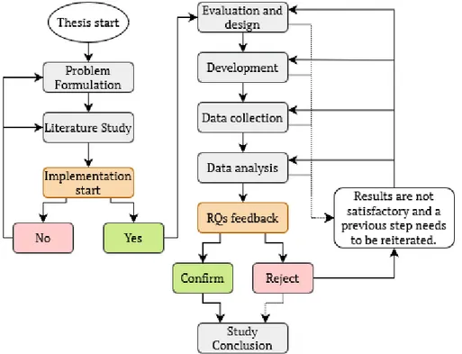
The following section describes the methodology that is followed in this thesis. Figure 1 shows this process in a flow chart. Continuous validation and testing of the work is performed in the implementation process with the option to reiterate previous steps if necessary. The thesis work examines two approaches with the same goal; one based on magnetic near field measurements and one based on IR image analysis. The two approaches are investigated in parallel, and the outcome is used for either cross reference between the approaches, or to draw a more extensive conclusion.
Figure 1: A flow chart describing the engineering design process that is followed throughout this thesis
work.
Problem statement
A problem is provided by the company, NEP. A problem formulation and research questions are derived and can be found in Section 3.
Literature study
This thesis involves several fields of practice, which is why a broad literature study is first con-ducted. Many studies have been made regarding the field of classifying images, both in the visible spectra and IR spectra. It comes down to choosing a classifier best suited for this thesis work. To be able to understand near field emissions, literature regarding basic knowledge of the EM radi-ation as well as literature regarding state of the art are reviewed. A method for measuring the magnetic near field is and carried out with the use of GMR sensors.
Evaluation and Design
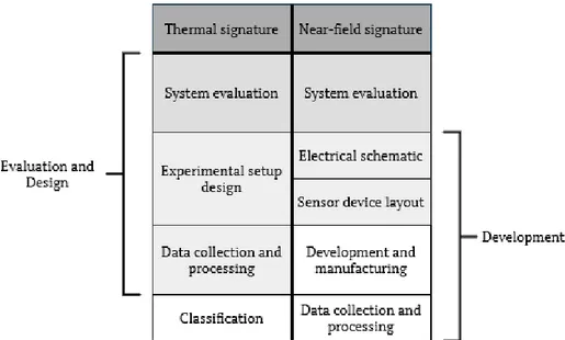
In the process of evaluation and design, a method for classifying thermal images is chosen and implemented using MATLAB software [44] and a process for repeatedly collecting images in a controlled environment is designed. Parallel to the development of the classifying algorithm GMR sensors are evaluated and most promising sensors to analyse the magnetic near field is then used to design the proposed PCB based measuring device. The circuitry and design of a sensor device is developed that can repeatedly collect measurements of a PCB’s near field.
Figure 2: Process of evaluating, designing and developing the two methods for PCB fault detection. The
left half of the figure represents the steps carried out withing the thermal signature method and the right half represents the steps for the GMR sensor approach.
Development
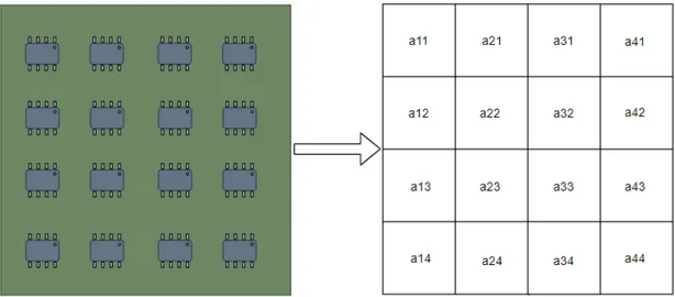
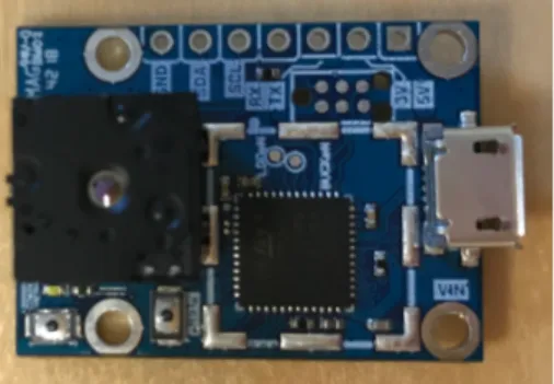
The method of collecting IR thermal images starts with an investigation of what cameras can be used, followed by developing a method of repeatedly collecting images. For the development of magnetic near field measurements, both the electrical schematics and a PCB layout are created using a software suite called KiCad. A process flow for the design and development phases can be seen in Figure 2. The proposed device for measuring the near field features 16 detectors. An example measuring device layout can be seen in Figure 3 utilising the GMR sensors. Several com-panies exist which offer PCB manufacturing services at low-cost1that can be used to manufacture prototypes of the measuring device.
Data collection
Both fault-free and faulty PCBs are used in the data collection process. The PCBs are driven in normal operating conditions. The measuring device is used for measuring magnetic near field of a PCB, and a FLIR thermal camera is used to collect images in the IR spectrum. The acquired data is transferred to and analysed in MATLAB.
Data analysis
The data from the thermal image is analysed and classified with a classifying algorithm to see if it is possible to distinguish faulty and fault-free PCBs with the thermal fault detection method. Data from the magnetic near field measuring device is analysed with the help of a machine learning algorithm.
Figure 3: Proposed magnetic near field measuring device that measures, with GMR sensors, several points
on a PCB and inputs these values in a matrix that can be interpret as a digital image.
Study Conclusions
Conclusions are drawn from the results, parallels and correlations between the two proposed methods are examined and presented in this thesis report. The correlation between results and research questions are discussed, and a conclusion is made about the outcome of this thesis work.
6.
Implementation
The following section describes the implementation work. As the thesis work addresses two dif-ferent methods of non-contact PCB fault detection, the implementation process has been divided into three separate parts, and is organised as follows:
6.1- Description of the DUT
6.2 to 6.10- Thermal signature implementation work
6.11 to 6.12- Magnetic near field implementation work
6.1.
Device under test
The device under test is referred to as DUT in the experimental processes. It is a PCB developed and designed by NEP, produced by an external company and then again tested and validated by NEP. The DUT is a populated with several components and is meant to drive an ultra-violet (UV) light bulb mounted in a refrigerator, to prevent bacterial growth. The circuit is designed to keep the output at fixed power, rather than a fixed voltage or current. To properly test these PCBs before delivery to the customer, NEP has developed an ICT specified for this PCB design. This ICT encloses the DUT and cannot be modified or used in this thesis because it needs to be available for NEP’s tests of their PCBs. Therefore, a more straightforward method of testing approved by NEP is first to test the PCB in an ICT to determine its functionality and run in close to normal operating condition using a dummy load. The dummy load is constructed with a constant resistive load on the 6 channel output of the DUT for the ability to make reproducible measurements, which is the same way the DUT is run in the ICT. The 6 channel output of the DUT each outputs approximately 7.2 kV at 104 mA, yielding a fixed power of 750 mW.
DUT # Reference Name Fault 1 Fault-free1 None
2 Faulty1 Unknown
3 Faulty2 Multiple
4 Faulty3 Transformer (L2) broken
5 Faulty4 Transformer (L2) broken
6 Fault-free2 None
Table 1: A list of the provided DUTs numbered 1 - 6 with thier statuses determined and displayed with two
of them being fault-free and four of them being faulty. #5 and #6 is the same PCB, before and after being repaired.
NEP have provided five PCBs to use in this thesis work. These PCBs are listed in Table 1 and the functionality of them have been determined with an ICT by NEP. The PCB listed as #5 was fault-free, but due to mishandling, a transformer was broken before any measurements could be done. This provided the opportunity to make measurements classified as ”faulty” before the PCB was repaired again. Measurement on #5 is only carried out with the GMR sensor device. It is worth noting that after the broken transformer was replaced, the card has been assumed to be working fault-free but this has not been validated.
6.2.
IR thermal imaging
An IR thermal camera measures the radiation within a specified wavelength interval of any sur-face, where each pixel of the thermal image represents a temperature value. IR thermal camera captures the level of IR radiation radiated from a surface over each point over the pixel in the im-age. When representing a thermal image on the application, the temperature is often translated into an RGB image with a different colour palette to easier locate heat anomalies. Two common colour palette used for RGB representation is called Ironbow and Rainbow, where Ironbow is rang-ing from black/blue to white/yellow and Rainbow is rangrang-ing from blue to red. Another common
thermal image representation is the greyscaled White hot palette that has a more linear visual heating representation as it is ranging from black to white [45].
Thermal IR cameras often perform image processing where the temperatures in the image are normalised to fit the colour palette. For the Ironbow palette the lowest temperature in the image is black and has the pixel value (0,0,0) and the highest being white (255,255,255) and in a greyscale image with pixel values ranging from 0 to 255. Two reasons do this, one to create a better visual representation and correct colour scaling of the thermal levels in an IR image and the other to im-prove the accuracy of the colour representation of the temperature. If for example, a camera with a range of -20 °C – 400 °C uses a greyscale palette with only 256 different colour shades. Without normalisation, the maximum resolution of the thermal image would be approximately 1.64 °C where the range of 420 °C is divided on 256, even though the camera may have better resolution than that [46]. The conclusion drawn from the use of these image processing is that it cannot be used for thermal comparisons between PCBs, because one colour representing a thermal value in one image may represent another value in another picture.
6.2.1 Multi-Spectral Dynamic Imaging technology
Multi-Spectral Dynamic Imaging technology (MSX) is by a patented method FLIR used to im-prove the thermal image representation with more contrast which is achieved through combining the visible light captured by a regular camera with the IR light captured by the thermal camera. Instead of just fusing the two images which may dilute the thermal image, the visual image un-dergoes feature detection and extraction before masking it on top of the thermal image. [47,48]. In Figure 4 the image captured by the regular, visual light camera of a FLIR ONE Gen 3, next to the thermal image captured with the regular camera covered. In Figure 5, an image captured with the thermal camera covered is displayed to show the feature extraction of the MSX and compared with the fused, MSX thermal image.
Figure 4: Images captured with a FLIR ONE Gen 3 thermal camera showing the visual image of the DUT
compared with an ironbow thermal image with the visual light camera covered.
6.3.
Thermal cameras
There are many different thermal camera products designed and used in many different applica-tions. FLIR Systems Inc is the world-leading company in the field of thermal imaging IR cameras, and have a wide variety of thermal imaging products [49]. This section presents a handful of different FLIR thermal imaging cameras that are available at a low cost, and their pros and cons for application in this thesis are presented.
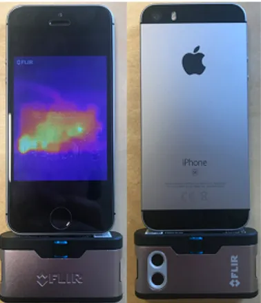
6.3.1 FLIR ONE
The FLIR ONE Gen 3 camera is a low cost easy to use thermal camera smartphone attachment and is shown in Figure 6. It is designed for simple applications or hobby use [50,51]. The FLIR ONE has a dual-camera setup with one thermal camera and on regular camera which is used for FLIR’s MSX technology. The thermal camera is a low resolution of 80x60 (4800 pixels), and
Figure 5: Images captured with a FLIR ONE Gen 3 thermal camera showing the visual image with feature
extracted representation of the DUT with the thermal camera covered, compared with the ironbow MSX image.
the regular camera has a 1440x1080 resolution. The camera can operate at temperatures of 0 °C – 35 °C and can measure temperatures of -20 °C – 120 °C [52]. Compared to the pro version of the FLIR ONE Gen 3 that has a thermal camera with a 160x120 (19200 pixels) resolution and 1440x1080 resolution lens of the regular camera. Its operating temperatures are the same at 0 °C – 35 °C, but the measure temperature range is -20°C to 400 °C. The FLIR ONE Pro has an image processing technology VividIR that improves the resolution of the thermal image with up to four times the pixels of the image captured from the thermal camera [53]. Although the FLIR one camera captures good images it i hard to capture stable images for comparison, because the camera has to be controlled with a smartphone and therefore, it is hard to get perfectly aligned images every time.
Figure 6: Front and back picture of a FLIR ONE Gen 3 thermal camera smartphone attachment connected
to a phone.
6.3.2 FLIR i7
The FLIR i7 camera is an older, handheld, easy-to-use, point-and-shoot IR camera with camera resolution of 140x140 (19600 pixels). It has an operating temperature range of 10 °C – 35 °C and a measurement temperature range of -20°C to 250 °C with an accuracy of±2 °C [54]. Figure 7 shows a test setup developed and evaluated for the FLIR i7 thermal camera. The same problem with getting perfectly aligned images every time is the same with this camera as with the FLIR ONE camera because a button has to be pushed on the camera to capture images.
6.3.3 FLIR Lepton
Figure 7: First version of the test setup with the constructed tripod fixture for the hend held FLIR i7 thermal
camera placed over the DUT.
on a PureThermal 2 FLIR Lepton Smart input/output (I/O) module breakout board [56] which is shown in Figure 8. The benefits of using this configuration are that it is possible to control
Figure 8: FLIR Lepton camera together with a PureThermal 2 FLIR Lepton Smart I/O module breakout
board.
the camera from a computer and use it together with MATLAB and not having to take images by hand which may interfere with the alignment of the images. There are several FLIR Lepton camera versions, with all versions before the Lepton 3 and 3.5 having a lower resolution of 80x60 (4800 pixels) and the Lepton 3 and 3.5 having a 160x120 (1920 pixels) resolution. All the FLIR Lepton camera versions except 2.5 and 3.5 have an operating temperature range of -10 °C to 80 °C and the measured temperature range is -10 °C to 140 °C. The 2.5 and 3.5 versions have an operating temperature of -10 °C to 65 °C and have a temperature range of -10°C to 400 °C. The FLIR Lepton 2.5 and 3.5 also have, by FLIR called, Radiometric technology where the value in each pixel in a captured image is a temperature value displayed in centiKelvin. The advantages of the Lepton cameras are that they can be controlled via a USB and may, therefore, be set up to avoid misalignment during and between testing.
6.4.
Flat field correction
Flat field correction (FFC) is a calibration method implemented on the FLIR Lepton and other FLIR thermal cameras. According to FLIR’s documentation for the FLIR Lepton thermal cameras [55], this calibration is performed because pixel values may drift over time and affect the image quality and temperature accuracy. With the default setting of the FLIR Lepton cameras, the FFC
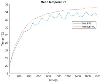
is performed every 3 minutes from last performed FFC and if a temperature change of a specified value occurs inside the camera (default 1.5 Kelvin). When capturing images of a heating PCB over time, the temperature data seem to be uneven. This is because the FFC calibration takes some time to finish and introduces a delay where the camera needs to refocus. In Figure 9, a comparison between measurements with and without FFC calibration is shown. The data displayed in the figure is collected from the two measurements that are acquired equally over the same PCB.
Figure 9: Data measurement differences between using FFC calibration and no FFC calibration of mean
temperature measurement of the DUT over 24 minutes with 60 seconds interval between measurements. Data acquired without FFC have more smoother curvature than the data with FFC enabled.
6.5.
IR test setup
Initially, the SIFT and SURF methods were proposed to align the thermal images perfectly. Due to the low contrast in thermal images and imperfections in these algorithms, a method of capturing near-exact images every time is developed with the use of the FLIR Lepton 3.5 thermal camera and the PureThermal 2 breakout board.
Figure 10: Test setup with the constructed fixture with the FLIR Lepton 3.5 thermal camera and
PureTher-mal 2 breakout board placed over the DUT at an opproximate distance of 100 mm.
The fixture constructed and shown in Figure 10, is built on a camera tripod [57] where the PCB holder and the camera holder are clamped down with screws onto the tripod’s centre rod. The
FLIR Lepton camera and the PureThermal 2 breakout board sits in a separate box that is glued onto the camera holder to sit in place. The camera holder, camera box and the PCB holder are designed in SOLIDWORKS [58] and 3D printed in polylactide (PLA) plastic.
Figure 11: Greyscaled IR image of a turned off DUT with the red line marking the borders which has to be
inside the image and should be covering as much as the image as possible for maximum resolution of the DUT.
The camera placement is approximately 100 mm above the DUT. The border of the DUT just inside of the frame of the Lepton camera, as shown in Figure 11 where the DUT covers most of the image with the red line marking its border. This way, the camera captures images the DUT at the highest resolution possible with as many pixels as possible covering the DUT. This is of greater importance when troubleshooting in specific areas and when using cheaper and lower resolution IR cameras.
The DUT is connected to a power supply, and dummy load output and the FLIR Lepton cam-era is connected to a PC with a USB cable. When initially starting up the camcam-era, the camcam-era auto-calibrates itself with FFC. The camera settings are then set inside MATLAB to not perform FFC calibration during testing. This is because the acquired data should not contain uneven mea-surements that may be caused by the FFC, as stated in the previous section and shown in Figure 9. Because the goal of the tests is not to measure the exact temperatures but to analyse the tem-perature differences, it is better to have the same calibrations of the camera for all images.
6.6.
IR data acquiring
Before the data acquiring, session starts the DUT should be turned off and cooled down to room temperature. The data acquiring is performed through MATLAB and is done by capturing images of the DUT. First, the user inputs the number of images and the time interval between each image for the session. The session is then started by pressing a button in the MATLAB script and with a second of delay powering up the DUT. The first image is taken just before the initial startup of the DUT and is used as a calibration image for later image pre-processing. The following image capturing sequence is then proceeded according to the user input. After the acquiring session is completed, the data is saved as a cell-matrix with each cell containing the value matrix representing the image of the DUT, which is a 160x120 matrix of temperature values. A visual representation of the temperatures of the DUT over time is presented in Figure 12.
6.7.
Pre-processing
The pre-processing of the raw data from the thermal camera is done in two stages. The first is to convert the raw, temperature data into degree Celsius. The second pre-processing is performed to properly align all data in a data set and prepare them for comparison between each other.
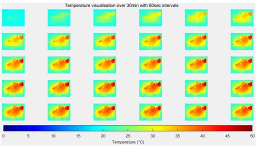
Figure 12: Rainbow coloured temperature visualisation of a known fault-free PCB over 30 minutes with
60 seconds interval between each image.
6.7.1 Temperature conversion
The raw images retrieved with the FLIR camera is a matrix with the pixel values (160x120 matrix for FLIR Lepton 3.5). According to the user documentation for the FLIR Lepton camera [59], for raw image data from the FLIR Lepton 2.5 and 3.5 cameras, each value of the image matrix rep-resents the temperature of the pixel at the measured surface. The temperature value is presented in centiKelvin, and the conversion to degree Celsius is, according to the documentation, called TLinear and is as follows:
TC=
TcK
100−273.15 (9)
Where TCis the temperatures in degree Celsius and TcKis the temperature in centiKelvin that
is divided with 100 to convert the value to Kelvin. Lastly, a conversion from Kelvin to degree Celsius is done by subtracting the difference of 273.15 between degree Celsius and Kelvin. All IR data acquired in this thesis is always converted right away inside MATLAB according to equation 9 for every element in the image matrix. The output is a 160x120 matrix with temperature in degree Celsius of the surface in each pixel of the image [59].
6.7.2 Data set alignment
The second pre-processing step is performed after all data has been acquired for a data set and is done because of differences in calibrations between data acquiring sessions. When new data is being acquired, the FFC calibration is performed on startup and stays the same throughout the whole data acquiring session. By retrieving a calibration image before the DUT has powered on, the differences in calibrations between measurement data in the data set can be calculated and subtracted for all images in the measurement data to line up all the data in the data set.
The pre-processing is performed on a complete data set where one measurement data is cho-sen as a reference. First, the mean value for all pixels in the first calibration image from all mea-surement data is calculated. Then the mean value difference between the reference data and all the other data is calculated. This value is an approximate difference in the calibrations between different data collection sessions. The mean difference is added to all pixel values of all the im-ages in all the data in the data set. This results in the mean value of all data starting at the same value and the heating curvatures can be displayed and compared. In Figure 13, the difference between the mean values of a data set before and after this pre-processing stage is displayed. The validation of this pre-processing method is done by observing the similarities of the data acquired from the fault-free PCBs. The drawback with this pre-processing step is that temperature values
Figure 13: Mean temperature of PCBs in a data set during 30 minutes from startup displaying differences
between the same data before and after aligning pre-processing. The curvature has not changed, but the starting point of all the data has been aligned to the same starting point.
may be incorrect, but in this thesis, the goal is to observe the heating differences and not the exact temperatures of PCBs.
6.8.
Clustering
Detecting faults in a PCB by analysing the temperature differences might be challenging. Finding variations in temperature in small areas or on a component level on the PCB by analysing the whole image in one piece. It may be hard to spot differences when comparing temperatures pixel-wise. Therefore, clustering is applied to remove unnecessary parts of the image. Parts that are outside the DUT and the areas of the DUT that do not change significantly in temperature. The clustering is also used to cluster the DUT itself into smaller critical parts that are easier to analyse separately.
The clustering is done with the MATLAB function ”imsegkmeans” which is an image seg-mentation that uses K-means clustering to create a numbered cluster of the image where the user chooses the number of clusters. The image is divided into clusters, and the image’s pixel values close to each other are assigned to the same cluster. In application with an IR image, the clusters are created with temperature values that are close to each other. Compared with image segmen-tation where the image is filtered with the clusters to create a low-resolution image with less and essential data, the clusters are only used to divide the image into separate images of the clusters, but still keep all temperature information.
Figure 14: Examples of clustering choices of clustering performed on images of the DUT over time during
The fault detection is done by comparing reference data from a known fault-free PCB and therefore, the clusters used on all the tests are created from this PCB. When creating the clus-ters, an appropriate clustering is chosen from an implemented MATLAB script where a different number of clusters are compared at a different point in time for the heating of the DUT. After the cluster data is acquired, several clustering alternatives of the DUT is displayed, and the most appropriate clustering is chosen by the user. Figure 14 shows some examples of how different clustering may look.
Figure 15: Example of a scattered clustering compared to the PCB component layout where a critical
transformer of the PCB is highlighted.
Figure 16: Example of a good clustering compared to the PCB component layout where a critical
trans-former of the PCB is highlighted.
If a cluster is scattered compared to the component layout of the PCB where the clusters do not cover entire components that are critical, temperature deviation may be hard to locate. An example of a scattered clustering is shown in Figure 15 where many components, for example, the transformer inside the red ellipse are poorly covered by one single cluster. Compared with a good cluster, as shown in Figure 16 where a single cluster fully covers the critical components. The clusters are also used to remove parts of the image that is not part of the DUT and to remove these; the clusters must cover the frame of the DUT according to Figure 11.
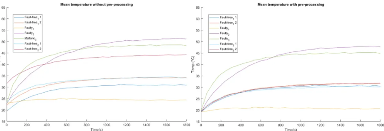
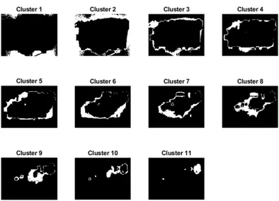
After an appropriate clustering is chosen, they are arranged in numerical order from the coolest to the warmest according to their mean temperatures. In this thesis, a clustering with 11 clusters of an image captured of the DUT when it has been running for 24 minutes is chosen. These clusters are shown cluster by cluster in Figure 17.
The outlying clusters that are not covering the DUT are then removed from the cluster set since the temperature in these areas of the image is not changing significantly over time. These clusters are set to 0, and the remaining clusters are rearranged again in numerical order starting from 1. The remaining clusters after this process are shown in Figure 18.
When dividing the image into clusters, one by one, the content of each cluster is set to 1, and the rest are set to 0 and is multiplied with the temperature image. This way, the image is split into multiple images with the shape of the chosen clusters; also, one image for the whole DUT with all the clusters included is created. The cluster visualisation with temperature visualisations of a pre-heated PCB is shown in Figure 19.
6.9.
Data analyse
Figure 17: All clusters separated in individual images, with the white parts is the area of the cluster in each
image.
Figure 18: The remaining clusters after outlier removal where cluster 1, 2 and 3 from Figure 17 have been
removed removed. The white parts is the area of the cluster in each image.
sampling frequency which is the image capturing interval. When analysing a data set the mean temperature is displayed over time as a graph, one graph for each cluster and one graph for the mean value of all clusters together. This is shown in Figure 20.
In theory, a faulty PCB’s temperature and the heating curve should deviate from a fault-free PCB. Therefore, by displaying the signature of the DUT next to the signature of a known fault-free PCB, the functionality of the DUT should be able to be determined. If in this test, the comparison is equal or similar, the DUT is considered to be fault-free, and if the correlation deviates too much, it is considered to be faulty. In some cases, the heat difference of a faulty PCB may be minimal, and it may not be possible to classify it from only comparing the mean temperature of the whole DUT. Thus, the test includes finding the temperature differences for each cluster and compare those among faulty and fault-free PCBs. With the thermal signatures of all the test boards displayed next to each other, the rest results may be validated. If all fault-free PCBs may be distinguished from the faulty ones, the test is sufficient for this set of PCBs. If not, the test has to be revised with either redesigning the data acquiring or improving the resolution of the tests by remake the clustering and add more clusters for comparison.
6.10.
Machine learning classification of IR images
The objective of this thesis is to binary classify PCBs and determine if they are fault-free or faulty and this is achieved with a CNN implementation. The training of the CNN is done with several thermal images of every PCBs during their heating process. The goal is to train the network to classify any image that has the same thermal signature and the same heating curvature as a
fault-Figure 19: One example of a thermal image divided into clusters. Cluster wise, rainbow coloured
visuali-sation of a powered PCB at one point in time.
Figure 20: Temperature graphs of all individual clusters and all clusters combined of a known fault-free
PCB over 30 minutes with 60 seconds interval between each data point. Showing the mean temperature of all clusters, individually and together, in separate graphs.
free PCB and any other as faulty. The CNN architecture is based on the CNN ResNet-50, which is imported and trained in MATLAB by following instructions from MathWorks where a CNN with five classes output classification is implemented with the same architecture [60]. The full process, including pre-processing, CNN training, validation and classification result, is shown in the flow chart in Figure 21.
6.10.1 Image pre-processing
When data is acquired with the FLIR Lepton camera, it is not initially represented as an image but a 120x160 matrix of temperature values. When a series of data matrices have been acquired for the machine learning data set, they are first converted into a greyscaled image where the values of the matrices are equally normalised into integers between 0 and 255 before it can be represented as an image. The second pre-processing stage is to mask out the DUT from the image according to Figure 11. This is done by removing the outlier clusters according to the clustering technique described in the section 6.8. and using all the remaining clusters as a mask for the image, as shown in Figure 22.
Figure 21: Flow chart describing the pre-processing of the CNN training and classification validation
starting with a data set of acquired thermal data that has been pre-processed with temperature conversion and data alignment. Following with pre-processing to fit the CNN divided in one part which is performed before importing the data into the network and one that is preformed inside the CNN.
Figure 22: A greyscaled image before and after pre-processing where parts of the image that do not belong
to the DUT are removed, where data value in outlier clusters have been set to ”0” which is represented as black in the image.
images are greyscaled 120x160, the pre-processing settings for the input to the CNN are set to ”grey2rgb”, and the network automatically resizes the images to the correct pixel size.
6.10.2 CNN training
Before the training of the CNN is performed, the data set has to be split into two sets, one for training Train set and one for accuracy validation Validation set. The data set contains multiple images of the same PCB and to get a valid classification result; it is crucial to split the training and validation set so that no images from a PCB that is in the validation set is used to train the network. The classification of the data is assigned to Fault-free for all the images of a fully functional PCB and Faulty for all images of a faulty PCB.
6.10.3 CNN classification and validation
After CNN has been trained, the validation set is sent through the network and classified by it without knowing the actual class of the images. The predicted classes for each image in the validation set are then compared with the actual classes, and the prediction accuracy can be de-termined.
6.11.
Magnetic near field fault detection
In order to investigate the possibility to use the magnetic near field measurements of a PCB for fault detection, a device consisting of 16 AAH002-02 sensors have been designed. Below follows the process of choosing the most suitable sensors, amplifiers and design of the GMR sensor device. Several sources of noise have to be considered in the evaluation system setup; the system is constructed on a breadboard, and the power supply used to power both the amplifier and the sensor might induce noise to the system.
6.11.1 Analogue GMR sensors evaluation
NVE Corporation [21] offers four subtype sensors in their AA-series of analogue GMR sensors, three of these are considered in the evaluation; the standard type AA002-02, the low-hysteresis
Figure 23: An overview of the system used to evaluate the sensors. The signal from different sensors are
amplified with an instrumentation amplifier, INA826 and then sampled with a Teensy 3.6. The sampled signals are sent to a computer and processed in MATLAB.
type AAL002-02 and the ultra-sensitive type AAH002-02. Some parameters are displayed in Table 2. The sensors are encapsulated in SOIC-8 packages, making them suitable for the PCB type application considered for the measuring device.
Parameter AA002-02 AAL002-02 AAH002-02 Field Sensitivity HIGH HIGH VERY HIGH Operation Field Range HIGH MEDIUM LOW
Hysteresis MEDIUM LOW HIGH
Table 2: Parameters from the GMR sensor datasheet. Operation field range is not an important parameter
as the sensors are meant to operate within the magnetic near field of the DUT. High hysteresis are inherent in magnetoresistive sensors, especially in the ultra sensitive type.
The sensors are tested with the system described in Figure 23. A signal generator is used to produce a square wave with different frequencies through a large shunt to test the at which fre-quency range the sensors can still produce an output. A DC power supply is used to produce a current, ranging from 0−3 A through the same shunt to see the output correspondence to differ-ent levels of the measured currdiffer-ent. The sensors are placed approximately 2 mm from the surface of the shunt, and 8000 data points are collected at 350000 samples per second (350 kS/s). Square waves are generated with 20 Vppat 20 mA AC in the frequencies 1 kHz, 10 kHz, 50 kHz and 100
kHz. The output from the measurements at 50 kHz and 100 kHz can be seen in Figure 24 and Figure 25. In each figure, the left plot corresponds to the output from AA002-02, middle plot cor-responds to AAL002-02, and the right plot corcor-responds to AAH002-02. At the frequencies 1 kHz, 10 kHz and 50 kHz, the ultra-sensitive sensor AAH002-02 produce a considerably higher out-put than AA002-02 and AAL002-02. The outout-put from the sampled square wave starts to become under-sampled between 50 and 100 kHz, which can be seen in Figure 25.
When testing the current range, 8000 data points are collected at 350 kS/s, and a mean value is computed from these measurements for each level of current. Figure 26 shows the output from each sensor in the ranges 0−0.3 A and 0−3 A, and in Figure 26a the range 0−0.03 A. In Figure 26b around 2.4 A, the output from AAH002-02 (blue line) starts to clip, which is due to the amplifier starting to reach the upper limit of the dynamic range. As expected, the ultra-sensitive sensor AAH002-02 has a much larger response to the current levels, and this can be seen as a steeper curve in Figure 26a and Figure 26b. In Figure 27, notice the scale of the y-axis; over the range, 0−0.03 A the difference in output corresponding to 0 A and 3 A for the sensors are approximately 9 mV for AAH002-02, and 0.4 mV for AAL002-02 and 3 mV for AA002-02.
An important factor that has to be considered when taking measurements with any of the mentioned sensors is the fact that there is a considerable amount of offset when a magnetic field is not applied, this is due to both the earth’s magnetic field and the residual magnetisation of the sensors [22]. This means that the ferromagnetic layers do not return to an original position after being exposed to an external magnetic field. The residual magnetisation is more prevalent in the