M
CEL505
GOVERNOR ELECTRONICS FOR DIESEL ENGINES
High availability pla orm for real- me control and advanced
fuel efficiency algorithms
Author:
Johnny Holmström
jhm07003@student.mdh.seUniversity Supervisors:
Prof. Lars Asplund
lars.asplund@mdh.seAss. Prof. Mikael Ekström
mikael.ekstrom@mdh.seCompany supervisors:
M.Sc Tomas Lindqvist
tomas.lindqvist@qtagg.seProf. George Fodor
george.fodor@qtagg.seArne Löfgren
arne.lofgren@qtagg.seJuly 15, 2013
Västerås, Sweden
Abstract
Fossil fuel is a rare commodity and the combus on of this fuel results in nega ve environmental effects. This paper evaluates and validates the electronics needed to run intelligent algorithms to lower the fuel consump-on for commercial vessels. This is dconsump-one by integra ng advanced fuel saving func consump-ons into an electrconsump-onic device that controls the fuel injec on of large diesel engines, as known as a diesel engine governor.
The control system is classified as a safety cri cal system. This means that the electronics needs to be de-signed for fail safe opera on. To allow for future research and development, the pla orm needs flexibility in respect to hardware reconfigura on and so ware changes, i.e. this is the basis for a system that allows for hardware-so ware co-design. For efficient installa on and easy commissioning, the system shall allow for auto-calibra on combined with programmable jumper selec ons to a ain a cost effec ve solu on.
The computa on of the fuel saving algorithm require accurate data to build a model of the vessels mo ons. This is achieved by integra ng state of the art sensors and a mul tude of communica on interfaces. Among other things gyroscopes contra accelerometers where evaluated to find the best solu on in respect to cost and performance.
This design replace the current product DEGO III. The new product requires the same func onality and shall allow for more func ons. Focus has been spent on communica on, methods of accruing sensor data and more computa on speed. In crea ng a new genera on of a product there are tasks like selec ng components, ques-ons pertaining to layout of the printed circuit board and an evalua on of supply chains. The manufacturing aspects are considered to ra onalize produc on and tes ng.
Document version
Version Date Note
1.0 2013-05-08 Ini al release
1.1 2013-05-15 Proof-reading
Table of Contents
1 Acknowledgments 5 2 Introduc on 6 2.1 Background . . . 6 2.2 Legacy . . . 6 2.3 Scope . . . 6 3 Purpose 7 4 Method 8 4.1 Workflow . . . 84.2 State of the art . . . 9
4.3 So ware . . . 10 4.4 Thesis output . . . 10 5 Design 11 5.1 Architecture . . . 11 5.2 Power supply . . . 13 5.3 FPGA . . . 14 5.3.1 Memory set up . . . 14 5.3.2 Decoupling capacitors . . . 14
5.4 Input and output . . . 16
5.4.1 Digital inputs . . . 16 5.4.2 Digital outputs . . . 17 5.4.3 Analog input . . . 18 5.4.4 Analog output . . . 19 5.4.5 Tacho input . . . 21 5.5 Galvanic isola on . . . 21 5.6 Failure indica on . . . 21 5.7 Digital selec on . . . 21
5.8 External Interface and buses . . . 22
5.8.1 Debug op ons . . . 22
5.8.2 Ethernet . . . 22
5.8.3 RS485 . . . 22
5.8.4 CAN . . . 22
5.8.5 I2C . . . 22
5.8.6 Serial Peripheral Interface Bus . . . 23
5.8.7 USB . . . 23
5.9 Touch interface/screen . . . 23
5.10 Iner a measurement . . . 23
5.11 Autonomous func onality . . . 23
5.11.1 Automa c tes ng . . . 23
5.11.2 Automa c calibra on . . . 24
5.12 Safety cri cal func onality . . . 24
6 Implementa on 25
6.1 Computer aided design . . . 25
6.1.1 Components crea on . . . 25
6.1.2 PCB schema c . . . 25
6.2 Produc on prepara ons . . . 25
6.2.1 Component selec on . . . 25 6.2.2 PCB Layout . . . 26 6.3 Prototype . . . 26 6.4 Tes ng equipment . . . 27 7 Verifica on 29 7.1 Digital out . . . 30 7.2 Digital in . . . 30 7.3 Analog out . . . 32 7.4 Decoupling model . . . 34 7.5 Supply voltage . . . 36 7.6 PWM input . . . 40
7.7 Earth fault detec on . . . 42
7.8 CAN . . . 43 8 Results 44 9 Discussion 46 10 Future work 47 10.1 Electronics . . . 47 10.2 System integra on . . . 47 10.3 Further tes ng . . . 47 10.3.1 Field tes ng . . . 48 10.3.2 Cer fica on . . . 48 References 50 Appendix A Logbook 51 Appendix B Simula ons 52 B.1 Digital switches . . . 52
B.2 Digital input . . . 53
B.3 Power filters . . . 54
Appendix C Thesis Specifica on 58
Appendix D Circuit diagram 63
1 Acknowledgments
During this master thesis there has been support and help. Apprecia on bestow Q-TAGG for support in re-sources and trust. Jörgen Bosson has been a great resource during the project examining solu ons and im-plementa ons. A special thanks is given to Lennart Lindh for his advisement. Per Lenander did a splendid job on se ng a standard and explaining his work in the preliminary inves ga on. Large apprecia on is given to Cograpro in Gothenburg, Sweden and Würth Elektronik in Germany for their advice on PCB manufacture. Elek-tronik Mekanik in Västerås has given helpful comments on component selec on and assembly. Mar n Ekström is recognized for many s mula ng discussions. A final men on goes to Bobo Lillqvist, Andreas Domfors and Thomas Pe ersson for reading the first dra of the report.
2 Introduc on
2.1 Background
A diesel engine fed on a steady flow of fuel will con nue to increase its revolu ons per minute un l it breaks down or where a steady undetermined state is reached. This is one of many factors that have to be regulated in a diesel engine [Figure 1]. Other factors are pressure for fuel injec on, individual load (if a system operates on several separate Diesel engines), safety aspects and much more. A device known as a governor is used to regulate machines like diesel engines. These are safety cri cal applica ons that need specific considera ons. During the last two decades there has been an increasing interest in using advanced sensors and digital solu ons to op mize the run of diesel engines. This theses expand and evaluate different aspects of the electronic hardware to such a solu on. Capable of delivering sensor data and computa onal power to run and evaluate complex models for fuel saving.
Figure 1: The system applica on opera ng four generators and two twin engine setups.
2.2 Legacy
The task of this thesis is to modernize an exis ng governor called DEGO III (Diesel Engine Governor III, [Figure 2]). The DEGO family have been developed during some thirty odd years.
• DEGO S
Was a system using an analog electronics pla orm to regulate diesel engines developed in the 70's. • DEGO II
DEGO S was improved into DEGO II. • DEGO III
The pla orm developed during the mid 90's is a digital version of the DEGO II. The system consists of two electronic boards (Termina on board and processor board) connected by a cable. The boards support the so ware func onality fully as of today. DEGO III runs on a micro-controller were all of the signal processing is made outside the processor proper. This system is used as founda on for this thesis and all the design documenta on and schema cs are made available.
2.3 Scope
The scope of the thesis is to create and adapt a more modern electronics system where the so ware runs on a FPGA so -core. The new system is refereed to as DEGO IV where the two boards of DEGO III are replaced by one board. A fundamental concept in crea ng DEGO IV is to reduce size, cost and complexity of the electronics. Examples of topics of interest are safety cri cal aspects, Iner a measurement, digital I/O, analog I/O and supply voltage stability.
Figure 2: DEGO III
3 Purpose
Q-TAGG R&D have an patented solu on for lowering fuel consump on on large commercial vessels. This thesis was created for evalua ng and crea ng an experimental embedded system capable of running this patented solu on. The new design is supposed to support the advanced func ons needed for this fuel op miza on. The details how the hardware will be used to achieve the fuel saving is s ll classified and will not be discussed in this thesis. Research aspects of this task was to evaluate the use of a FPGA in a Safety cri cal applica on, evaluate accurate hardware for measuring iner a and finally create a flexible pla orm for future changes, were there is a high demand for a pla orm that is programmable and auto-calibra ng.
4 Method
4.1 Workflow
The documenta on primarily consists of the thesis report. The report served as a development tool were ideas were developed and also shared among supervisors, during the final phase of the thesis the results were documented. The report were con nuously updated, showing the latest progress. This thesis is divided and documented in separate phases. First is the method describing how the thesis was performed. Following the method is the design (Sec on5) where different possible designs to solve the problem are discussed. This dis-cussion leads to the implementa on (Sec on6) where the manufacturing of the PCB´s is documented. Finally the results are presented followed by the conclusion of these results (Sec on7).
During the thesis a GANT schedule was used as the primary tool for planning and viewing deadlines. The deadlines should be considered as so -deadlines. Different stages in the thesis do overlap and run in parallel. During the first two weeks of the thesis there was none or li le research and the design mediates a func onal-ity rather than a solu on, details are le as assump ons or unanswered un l the Computer Aided Design (CAD) of the electronics begins. It is during the CAD process the design challenges are resolved. During this phase research and component selec on was done in parallel with the actual detailed design. There are however ques ons that need answering before the CAD is ini ated, therefore a work-flow is chosen as recommended by Altera for a design with FPGA devices [Figure3]1.
Figure 3: Work flow recommended by Altera, Image by Altera.
1Altera, "Ge ng started flow for board designs"
The phases can be broken down to: • Specifica on
Understanding the current system and new design requirements. • Method
Se ng up an efficient and construc ve work method. • Design
Making a rough new design based on a study of previous work. • Prototype
A final prototype is to be produced. • Verifica on
Verifying the theore cal design with measurements in the prototype. • Documenta on
In the documenta on phase the thesis work is more clearly described and edited. • Presenta on
In the last phase a thesis presenta on is prepared and presented.
4.2 State of the art
• Programmable
Making hardware se ngs controllable turns the focus to programmable hardware such as Field Pro-grammable Gate Arrays (FPGA), Field ProPro-grammable Analog Arrays (FPAA) and Field ProPro-grammable Mixed signal Arrays (FPMA) [8]. Other less advanced but efficient methods are digital poten ometers and MOS-FETs implemented as switches.
FPGAs have been in use for some me in systems where there is a need for either signal adapta on or hardware changes. FPGA technology is also ideally for running data processing in parallel. "An FPGA is a key component that is frequently used in complex system designs because of its programmable na-ture and integrated high-speed transceivers. Because of this flexibility FPGAs have become the central part of a flexible system, allowing designers to easily bridge different technologies and u lize both high and low speed signal processing."2. In these environments the FPGA have proven to be highly func onal
and there is an op on to run a so -core (an emulated central processing unit). In the DEGO IV there is a need to simplify the electronics design and to make the hardware modular.
Preliminary inves ga ons into FPGA technology for the DEGO IV were made resul ng in a selec on of language, tools, program structure and code. Very High speed integrated circuit hardware Descrip on Language (VHDL) was selected as the primary programming language (Hardware describing language) and Quartus became the chosen pla orm. A so -core system was setup to run so ware and IP compo-nents for hardware accelerated func ons. A FPMA seems to be advantageous compared to the FPGA but it is not yet commercially feasible.
• Auto-calibra on
The ambi on is to produce the DEGO IV without the need of manual calibra on. There are different type of basic circuitry that react and change the hardware to compensate offsets. Digital poten ometers or MOSFETs (floa ng gate transistors) are examples. In spite of the calibra on method there will be a need for a control loop measuring the circuit state like a redundant sensor [12] or measurement of current 2Altera, "Ge ng started flow for board designs"
and voltage. Using programmable hardware simplifies hardware calibra on, where FPMA creates a great pla orm for measuring and adap ng circuitry even during run me.
• Measurement of iner a
One of the requirements of the DEGO IV is to measures the angular posi on of the ship. This is achieved by installing the sensors such as accelerometers and gyroscope directly on the circuit board. Where Accelerometers measures the proper accelera on, gyroscope measures the angular velocity. There are different types of sensors such as mechanical-, piezoresis ve-sensors. The piezoresis ve sensors are in common use, where the MEMS based sensors have great advantages [9]. It is possible to determine both accelera on and angular velocity by using accelerometers [12]. This provides an accurate reading for a lower implementa on cost.
• Safety cri cal aspects
There are hardware and so ware requirements to ensure safe opera on. A system is defined as safety cri cal if a failure results in injuries of people, large damage to property or if lifes are at risk. There are aspects to be considered to maintain data integrity and system func onality in the safety cri cal system. A system not accep ng a single point failure causing a cascading common mode failure without redun-dancy could be considered to be a "weak system". These "weak systems" are more simple thus less prone to failure [3].
To ensure safety or to achieve redundancy there are some well known methods available. Fault-containment regions providing galvanic isola on to counteract cascading failure and interference. [3], Clock and power monitoring should be considered as a fundamental necessity [4].
To ensure correct processing of data within the processing unit there could be implementa ons of such methods as triple modular redundant architecture or dual lock step architecture that can ensure correct data processing by comparing the results [3]. Another important aspect in a mul -node system are the buses. There are many different bus standards such as Controlled Area Network (CAN), Ethernet, RS-485, SAFEbus, SPIDER, TTL and many more. The later men oned buses (SAFEbus, SPIDER, TTL) are me driven buses that are more suitable for safety cri cal applica ons [11]. An interes ng selec on is the SPIDER op cal bus, with its fully electromagne c immunity. If a fault is detected an alarm should relay this informa on to the user and the system should a ain a safe state as soon as possible.
4.3 So ware
There were some queries regarding the pla orm and work environment in the beginning of the thesis. Quartus and VHDL were already determined as the pla orm and language for the hardware describing code. For the electrical CAD there were some alterna ves inves gated, EagleCAD, Ul board and PADS. A er evalua ng the op ons and tes ng the interfaces PADS from Mentor Graphics was selected as the development tool. PADS was selected due to its compa bility towards quartus. The user interface and simula on capabili es seemed very good in both Ul board and PADS. Ul board is easily interfaced to Labview however PADS seems to have be er thermal analysis, which would render them as equal.
4.4 Thesis output
During the thesis the components defined in the thesis specifica on (AppendixC) is to be delivered. A report, a prototype and the func on is included in this specifica on.
5 Design
5.1 Architecture
The system func onality and layout is based on a design with low level of details. The top level design is then developed into more details during the research process. Some general proper es are important for the func onality of the overall design. Resistors and capacitors are set to a size of 0603 as recommended by man-ufacturer, this package is small and does not increase expenses nether does it render the targeted tolerance values difficult to reach [6].
The dielectric proper es are set to X7R for ceramic capacitors, resistors should be metal film or Metal foil due to their good temperature coefficients [14]. Size and dielectric property of components may vary in spe-cific cases. Tradi onal fuses are not to be used, they are replaced by thermistors due to their auto-rese ng proper es.
The DEGO IV system must have compa ble specifica ons to the DEGO III system (AppendixE). It is also im-portant to make the system easy to install and maintain. There are jumpers and pins in the DEGO III system that are designed for manual measurement, calibra on and setup. These pins have to be removed to sim-plify the manufacturing and procedures during installa on, without losing func onality or safety. The PCB is designed to maintain symmetry and electrical soundness according to reference documents on the subject3.
Trace length compensa on have to be considered in some of the high speed buses4. To get a good overview
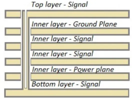
of the en re system a high level architecture block diagram was constructed [Figure4]. General condi ons are based on the IPC2221 standard5as in the case of layer stackup in a four layer PCB [Figure5] or a six layers PCB
[Figure6].
Figure 4: Block diagram of the FPGA system including interface and support func ons.
3David, L , J, "PCB Design Tutorial"
http://alternatezone.com/electronics/pcbdesign.htm
4Texas instruments,"High Speed PCB Layout Techniques"
http://www.ti.com/lit/ml/slyp173/slyp173.pdf
5The Ins tute for Interconnec ng and Packaging Electronic Circuits, "Generic Standard on Printed Board Design"
Figure 5: A four layer cross sec on of the governor PCB.
Figure 6: A six layer cross sec on of the governor PCB.
For connec ng the different layers there are via connec on. There are different types of vias [Figure7] where the vias are copper filled microvias. The A, B and F Vias were selected for connec ng the layers and supplying power. The vias can be placed directly in pads increasing the rou ng op ons and giving short paths to ground for decoupling and integrated circuits.
5.2 Power supply
The system will be fed by a 18V - 32V direct current supply. This voltage is to be broken down into a number of discrete power levels: 24V, 15V, -15V, 12V, 10V, 5V, 3.3V, 2.5V and 1.2V. In DEGO III there are exis ng power solu ons for some of these power levels. The solu on in DEGO III for fault monitoring the power levels and protec on from transients is accepted as it is with some reduc ons (see5.11.2). There are concerns regarding heat and efficiency in some of the voltage regulators. The LM2574 regulator is accepted as a regulator with good efficiency. The linear LM317L regulator and the in house developed step-down regulator for -15V is not accepted due to inefficiency on one hand and large amount of components on the other. The linear regulator is replaced with a LM2574 and the -15V will be regulated by the use of a integrated circuit (IC) TPS84259, this IC was released a couple of months ago (September, 2012). TPS84259 is an inverter with a wide range of input voltage and an output wa age of 15W. The TPS84259 does not require any external magne c components and only uses five passive external components giving a very low implementa on cost.
An early power es ma on showed low power requirements below 300mA for the FPGA [Figure10],
opto-cuplers of 200mA, control circuity use of 100mA and inputs and outputs of 1500mA, giving a total power re-quirement of 2,1A at different voltage levels. The TRACO DC-DC voltage converter for 12V supports galvanic isola on and deliver approximately 1A. Within the galvanic isola on area switching regulators regulate the power. To ensure a stable power supply to the FPGA some Low-Pass Filters (LPF) are introduced to the design. The filters were calibrated and simulated to remove harmful harmonics [Simula on:Appendix B].
An important part to protect the system from interference is to filter the main power. There are inductors for such filters, evalua on of the current solu on showed poten al for improvement. A flat wire inductor has be er proper es than a round wire one with a compact area, but the largest improvements are AC effec ve-ness, such as lower skin effect resul ng in a be er use of the copper cross sec on. Therefore there is li le difference using a flat-wire inductor or a round-wire inductor in a DC applica on. A common-mode inductor with a sec onal winding filters both differen al and common-mode interference effec vely and is therefore the best selec on.
5.3 FPGA
Many aspects of the FPGA are evaluated. Standardized solu ons are to be used as far as possible and reference designs will be incorporated into the design within copyright restric ons. The FPGA to be used is the Cyclone IV with FLASH, SRAM and a EEPROM. Design considera ons were made according to Altera and ISSI.6 Hot spots should be avoided to reduce failures from thermo-stress. Proper design is important at the BGA chip to avoid mechanical cracking in pads and vias [10]. 55% of PCB failures in aircra s are the result of overhea ng or thermal-aging according to Dave Steinberg [13]. This makes Thermal related ques ons the first priority for life expectancy. " A satellite in orbit around the Earth experiences a thermal cycle about every 90 minutes. In 20 years it can accumulate about 117,000 thermal cycles." Dave Steinberg. Making on site repairs is unprac-cal, the maintenance is limited to replacing the DEGO IV, a recommended opera on me of the DEGO IV is considered to be FPGA life me.
5.3.1 Memory set up
The selected memory set-up was chosen due to its simplicity. A 2 MB SRAM was selected as-well as a I2C EEP-ROM 512Kb memory. For the FPGA image and program code a 8MB Flash memory was added. The programing is done in Ac ve Serial Mode (ASM) by an Altera USB-blaster. A Serial Configura on Device (EPCS) is used, the EPCS then transfers the FPGA image during power up. During normal use the power up could be calculated based on the configura on me7of the FPGA. The configura on me can be calculated [Equa on 1], the DEGO
IV has 1 Bit/Clk.
DataSize∗ClkM ax
Bit/Clk = N anoSeconds (1)
5.3.2 Decoupling capacitors
Decoupling for the FPGA is a complicated task yet very important. To make a good es mate of the decoupling one needs good informa on of the system impedances (Z) and the maximum allowed system impedance
(Z-max) Z must at all mes be lower than Z-max [Equa on 2]. To determine The Z-max one needs to know the maximum current used by the system as well as allowable the AC ripple in percentage. For a FPGA these values are available in the documenta on. The Z-max is calculated [Equa on 3], [1]. The system impedance is very difficult to calculate but can be well es mated if parasi c effects on the impedance are kept to a minimum due to good PCB layout. If the clk is considered as the fundamental harmonic and the rest of the harmonics can be ignored and the decoupling can be es mated [Equa on 4].
A supplement method to compensate for changes in the impedance could be to place the resonances fre-quency of the decoupler capacitors with parasi c effects [Equa on 5] to cancel resonant frequency of the parasi c effects from trace induc on and die capacitance [Equa on 6]. There is an illustra on to view the idea of this hypothesis [Figure9]. It is important to remember that inductance reverses its effects a er the opera ng frequency passes the self-resonance of the system [15].
6These recommenda ons include but are not limited to documents such as
Altera, " Cyclone IV Schema c Review Worksheet",
http://www.altera.com/download/board-layout-test/schematic-review-ws/worksheets/Cyclone_IV_Schematic_ Review_Worksheet.doc
Altera, "CycloneIV Device Family Pin Connec on Guidelines",
http://www.altera.com/literature/dp/cyclone-iv/PCG-01008.pdf
Altera, "Cyclone IV Device Handbook",
http://www.altera.com/literature/hb/cyclone-iv/cyclone4-handbook.pdf. Altera, "I/O Management",
http://www.altera.com/literature/hb/qts/qts_qii52013.pdf. 7Altera,"Serial Configura on (EPCS) Devices Datasheet"
The previously men oned parasi c effects indicate to be the most influen al ones [1]. Other factors can how-ever be added to this calcula on to increase accuracy. For instance the plane capacitance can be added, and so on for be er results. Finally measurements on a prototype has to be done to answer if the systems impedance is properly within the limit of Z-max. For the DEGO IV Z-max is 252mΩ for the internal power (VCCINT) of the FPGA. Zmax > Z (2) Zmax = [ V oltageRail Ripple M axT ransientCurrent ] (3) C = [ 1 F∗Z 2π ] (4) F = 1 2π√Lcap∗ Ccap (5) F = 1
2π√(Ltrace + Lpackage)∗ Cdie (6)
5.4 Input and output
Input and output design will strive for an uniform solu on. Any adap on or filtering of one specific signal will be processed within the FPGA. These changes are all in the line with ambi on to simplify the hardware archi-tecture. Signals do have some differences. Signals are therefore divided into different categories. Transient protec on on I/O was first selected to consist of scho ky-diodes and zener-diodes but on recommenda on from an adviser this was changed to a transient voltage suppression diode due to high power absorp on and the good property that in the case of breakdown they goes to short circui ng thus protec ng the circuitry.
5.4.1 Digital inputs
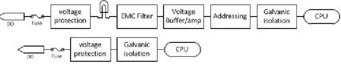
The system has a need for environment interac on by Digital Inputs (DI). The DI are required to accept signals in a range of 0V - 32V. In the DEGO III system design the signal will flow through transient voltage protec on, a LED indicator, cross cable jumping PCB from termina on board to processor board, signal filtering, current limi ng, signal selec on by mul plexing then finally before entering the Micro-Controller Unit (MCU), a layer of galvanic isola on. In the new design a few elements will be removed. This is due to the fact that there will be no cross cable jump and no limita on in number of inputs to the FPGA. The new and old signal flow can be seen in figure below [Figure10].
The largest change to the design is removing the mul plexing and adding a high input resistance of about 100kΩ. The input filter has been changed, the corner frequency has been moved to 1KHz from 10kHz. The filtering is be er despite fewer and smaller capacitors. The response me for the DI is unchanged for low fre-quency signals according to simula ons [Simula on:Appendix B] but as a result of heavier filtering there has been a larger phase shi at higher frequencies. It is difficult to es mate if the actual step response of the DI is improved or not.
5.4.2 Digital outputs
The Digital Outputs (DO) has a more complex design compared to the DI in the DEGO III design, where signals can be categorized in three subcategories. A new criteria is to make sure that all three signal types are com-pa ble to run with one new solu on. All DO in DEGO III are routed though a 8-bit addressable latch. This latch is no longer needed due to a higher number of general purpose I/O. The DEGO III design contained 4 channels that run through comparators then the signal is buffered by a transistor. There are 2 signals called Alarm1 and alarm2 that are routed directly to the termina on board and then powers internal logic for failures (Failure indica on [5.6]).
These two different types of channels are going to be replaced by one common type where the signal is routed directly to an output port or internal logic where the buffering is done directly by the galvanic layer. This will put heavy load on the galvanic isola on [Figure11]. Later es mates showed compromised stability of the signals, therefore it was decided that the four DO s ll needed a buffer, this was implemented by the use of MOSFET transistors. The last type of DO that transmits the signals for manual control. These outputs will experience some redesign but from a safety cri cal point of view they need to maintain the proper es of DEGO III. Manual control have an auxiliary power source and needs to support an external override no ma er the state of the CPU. This is further described in the safety cri cal sec on [5.12].
5.4.3 Analog input Design 1:
Analog Input (AI) converts an analog value to a Pulse Width Modulated (PWM) signal. The transla on is done by use of comparators. The input voltage during a short me frame is considered stable at a certain voltage level and the reference is varied as a triangular wave (the integrand of a square wave regulated from the FPGA). If these two signals are compared it would give a PWM signal output, see figure [12]. The ramp is generated by a dedicated circuit that will be redesigned and simplified: Previously in the DEGO III there was an analog circuit genera ng a square wave then integra ng it to a triangular wave. In the DEGO IV design the square wave can be generated by the FPGA.
There is a circuit calcula ng the phase shi between current and voltage, when the DEGO runs as a power generator governor. This design can be simplified and calcula ons can be done within the FPGA in VHDL. The AI can both measure voltage and current in DEGO III by se ng the mode with a a jumper. This jumper will be replaced with a digital switch in DEGO IV. Current measurement is done by grounding the signal with a resistor, the resul ng voltage is measured.
Design 2:
There is an op on to use an Analog to Digital Converter (ADC) to perform an analog measurement. There are a few different ADC components commercially available fulfilling the needs to support analog measurement of
±10V, DC and maintain current sensing of ±20mA. Evalua on:
Dithering [2] could be used if the environment is causing interference. The environment is free of interference elimina ng the use of dithering, even if the technique is highly interes ng. Using the first design, a signal from the FPGA to control the ADC PWM ensures a match in frequency. The complexity is lowered from DEGO III by using a FPGA and the PWM seemed like a good discrete approach. During calcula ons of the the ADC resolu-on, the PWM solu on showed a poor performance. Finally an integrated circuit was selected, AD7328 from Analog Devices. The selected circuit was an 12-bit, SPI controlled ADC with 8-channels and an range of±10V.
Figure 12: PWM signals are generated according to this principle.
5.4.4 Analog output Design 1:
The Analog Output (AO) can run as a voltage or current output. The design of the analog output from DEGO III will be kept intact as far as possible. There are a two new requirements that needs to be supported. The current output is stable by the use of two amplifiers that require manual calibra on of each board produced. The first requirement is to ensure no manual calibra on. The second new requirement is to eliminate a jumper at each output that sets the output range. This implies that the design needs a new configura on. For the first requirement there could be a way to handle the situa on by the use of one opera onal amplifier with high current ra ng. The second requirement could be handled by a digital switch much like the one discussed in AI (5.4.3). This all seems like a possible approach provided that an OP can be found that can provide a current of
± 20mA with sufficient resolu on. A new solu on was proposed simplifying the old one [Figure14].
Figure 14: Analog output: on top the DEGO III design with the proposed DEGO IV showed underneath.
Design 2:
During a one day seminar provided by Texas instrument a new idea was formed. A MCU could be used instead of using opera onal amplifiers and filters to convert the FPGA PWM output into a stable current. Such a MCU solu on could implement a switching regulator up to 5MHz. A closed control loop adjusts the voltage output level by sampling the output and then calcula ng the error to adjust the switching duty cycle. The solu on uses a Z-transform to implement a digital filter. In DEGO IV a real- me MCU could handle this, given a suffi-cient number of ADC and PWM ports.
In such a system the analog input signals would be provided by the MCU to the FPGA as a PWM signal. The analog output would be controlled by a MCU in the closed loop to ensure stable current output. This method limits the components of the Analog I/O to one MCU, three OP and three MOSFETs, with some surrounding passive components like a LC-filter [Figure15]. Because of safety cri cal reasons this solu on might not be possible to implement, specifically considering a lack of galvanic isola on. A possible compromise might be to use galvanic isola on transfering analog signals or using high input resistance.
Design 3:
Another method is to use an IC that is galvanically isolated like shown in [Figure16]. The solu on consists of a digital controllable amplifica on unit in the output range of +/- 15V. The output current is measured and a voltage is returned according to [Equa on 7]. This closed loop can regulate the current, it is programmable and can be implemented in the so - core or FPGA as VHDL. The resistance span for the load is increased from 50Ω - 500Ω to 25Ω - 700Ω compared to the DEGO III design. The manual jumper se ng for the current range is eliminated, in this way no calibra on of the circuit is needed anymore.
Another advantage is that the device drawing current can use a different neutral level without it effec ng the current being outpu ed, even if the resistance range will be changed. An exaggerated example is if the external device uses a neutral reference of 10V in rela on to DEGO IV, then the range of load would be 0Ω -250Ω. There was also a risk that the IC in design three only accepted AC signals, this was not evaluated. An-other disadvantage is that the cost increases from that of DEGO III. Values have been verified in a computer simula on [Simula on:Appendix B].
Design 4:
The last evaluated method was to use a biased transistor to regulate the current output. This solu on did not sa sfy the±20mA but delivered only a 20mA current.
Evalua on:
An evalua on was made based on func onality and complexity. The outcome was that the third design was considered the most flexible, func onal and easily manufactured solu on to the stated criteria. Due to pro-duc on costs this op on proved not to be op mal. To overcome this the requirement of±20mA was changed to 0 to 20mA. Two different outputs were selected for tes ng, a transistor based amplifica on unit and an integrated circuit with a transistor amplifica on with temperature compensa on (LT3092).
Figure 15: A diagram showing the proposed regula on loops for Analog I/O.
Figure 16: DAC solu on,using a regula on loop. Part of image property of TI.
I = V
5.4.5 Tacho input
The Tacho inputs of the DEGO III are well designed. With the FPGA technology we acquire the op on to move some func onality from digital electronics to the VHDL hardware descrip on. This enables us to eliminate the frequency divider and jumpers. The current and voltage transient protec on including hysteresis protec on can be kept from the DEGO III design.
5.5 Galvanic isola on
There are several op ons for galvanic isola on where opto-couplers or induc ve iCouplers are the two primary selec ons. There are some criterias to fulfill:
• Preferably they should be in PCB manufactures stock as a standard component. • There should be several IC manufactures.
• All isolators should be of the same type and part number. • Frequency supported has to be at least 13,5kHz.
• Long life expectancy.
The first two points were fulfilled by the opto-coupler but the other requirement are be er met by the Icoupler with a life expectancy of 50 years and with higher opera onal frequency. A opto-coupler can handle a large voltage as long as the current is limited. The Icoupler needs a fixed voltage of 2V to 5V and good flanks to work. Icoupler was selected due to its speed and life expectancy.
5.6 Failure indica on
The failure indica on on DEGO III is simple yet very effec ve. The func on is based on solid state relays. DEGO III uses an Array of NOT-gates for handling signal switching in a very cunning way. One could say it is a small piece of engineering art, sadly it increases the complexity of the board and it is therefore removed. DEGO IV uses the solid-state relay func on controlled directly by a control signal.
5.7 Digital selec on
In order to use dual func onality of some func ons like AI (voltage/current) or the voltage regulator se ng (fixed/adjustable), a hardware selector was needed. Currently manual jumpers are used, these should be re-placed with digital switches. Different requirements exist depending on the loca on of the switch. Primarily MOSFETs would be used as switches for the simplicity and low price. If a transistor should be used as a switch it should not operate in its ohmic state, but move as fast as possible from sub-threshold [Equa on 8] to ac ve mode [Equa on 9]. It is important that the MOSFET construc on fulfills these requirements to work properly. In some parts of the system a n-channel MOSFET is needed to power a P-Channel MOSFET. In some places the condi ons are insufficient to use one or two simple MOSFETs. In these places solid-state relays have been used. Switches have been simulated to ensure the func on and response me before manufacture. By these simula ons, phase shi has been minimized [Appendix B].
V gs < V th (8)
5.8 External Interface and buses
DEGO IV requires interfaces to be func onal. These peripherals include the digital and analog I/O for backward compa bility. There are also more complex interfaces necessary for normal opera on. There are interfaces necessary during run me and there are some needed for debugging and programming. Also Some buses for internal rou ng on the PCB and some buses that interact with external devices are required.
5.8.1 Debug op ons
There is a need to debug the system in development and in normal opera on. The main debugging is to be done by the use of an USB link, secondary debugging is done by a on-board 20 x 4 display with a parallel interface. In the future a touchscreen can serve as an on-board control interface (sec on5.9). This might even eliminate the need for a PC if the user wants a more integrated solu on.
5.8.2 Ethernet
Ethernet is a collec on of standardized methods for data communica on. DEGO IV is designed for compa bility with IEEE 802.38. This is implemented by the use of a Phyceiver handling the physical layer by communica ng
by Reduced Media Independent Interface (RMII). Originally a DMA9000A was intended to be used. This chip in-cludes the Sublayer for Media Access Control (MAC). The DMA9000A simplifies the so ware but limits the user. The design is verified to support 100BASE- TX. Ji er dampening and galvanic isola on necessary by IEEE802.3 is integrated in the RJ-45 Connector and supports BASE 1000 opera ons. DMA9000A was later replaced with a TI DP83848I.
5.8.3 RS485
The system needs two RS485 ports using a transceiver that connects to the bus. The connec on uses zener-diodes and filtering capacitors to sa sfy standards. The impedance in the transceivers is considered as very high and Pull-down resistors have been added. The transceivers (ADM2682E) are powered by the DEGO IV locally and are galvanically isolated.
5.8.4 CAN
The CAN connec on uses an isolated transceiver ADM3053. The design is equipped with protec ve circuitry and filtering by use of a common mode filter. The differen al pair have transient protec on by the use of zener-diodes that protect CAN-H and CAN-L from over +5V and nega ve voltage. Originally a digital switch would give a programmable op on to operate the transceiver on bus power or internally regulated power. Using the on-board power would effec vely interfere with the galvanic isola on. ADM3053 has a built in isolated DC-DC converter without an increased IC cost giving no disadvantage opera ng the CAN on a three wire interface. The construc on principle used is in line with normal praxis.
5.8.5 I2C
As described by the I2C specifica on9 this bus works as an addressed serial communica on link. There are
three buses available on the board, EEPROM uses one of these buses. Two buses are connected to external connectors resul ng in up to twenty op onal external devices can added to the system. The buses include pull-ups for data lines and series resistors to the devices according to I2C specifica on. The values for resistors in the external units are calculated according to 20 connected nodes. External units should use a 100Ω resistor in series on the CLK and data line to reduce noise while opera ng with twenty connected nodes. The I2C bus is configured for 3.3V devices.
8IEEE, "IEEE 802.3: ETHERNET"
http://standards.ieee.org/about/get/802/802.3.html
9Department of computer science, University of North Carolina, "The I2C-bus Specifica on"
5.8.6 Serial Peripheral Interface Bus
There are several peripherals in the system that are using a Serial Peripheral Interface Bus (SPI). The SPI is a four signal bus. Three buses are available for gyroscopes and two buses are reserved for ADC. There is one bus extended to a connector for external use.
5.8.7 USB
This interface was kept simple, an USB controller from FTDI UART- USB was selected. The communica on to the controller is a standard UART with signal pins RTS and CTS. Common mode filter was added to filter data lines but no external protec ve circuitry was added. The controller is internally powered from the board. The requirements for an USB self powered configura on are met10.
5.9 Touch interface/screen
There must be a method for interfacing and displaying output from the DEGO IV. To keep up with current technology and to make the interface user-friendly it has been decided that a touch-screen interface would be a good solu on. It is not within the scope of this thesis to design this interface. What is part of this thesis is to perform the necessary ac ons to allow this interface to be added at a later phase without the need to make design changes to the PCB. From discussions with consul ng a expert it was decided that I2C (Sec on5.8.5) or SPI (Sec on5.8.6) was a suitable hardware interface for this touchscreen. Another cost-effec ve and flexible solu on is to set up wireless access-points to interface tablets to ship control. DEGO IV will also support an 4x20 dot matrix display on a parallel and serial interface.
5.10 Iner a measurement
Based on the report by Christer Gerdtman et al. [7] good results of measuring quick movements was achieved by using gyroscopes in two axis. The MEMS based mouse in the paper operated using a CG-L43 NecTokin gyroscope. CG-L43 was for the DEGO IV unsuited due to the fact that there is a need for measurement in three axis with devices mounted on a PCB. A good alterna ve is the CRM200 Pin point and CRM100 Pin Point with its good performance and small size. These would measure rota onal speed very well, but due to the gyroscopes quality, the cost is high. There is an alterna ve solu on to use accelerometers that are cheaper and easier to acquire. It will require more work to get reliable rota onal data from these devices, but it is possible with filtering to acquire similar results.
5.11 Autonomous func onality
The DEGO IV system is designed to require low knowledge for the installa on and maintains. To ensure safe opera on there is a need for autonomous func ons that can test, monitor and calibrate the system. This will also lower produc on me and -cost as well.
5.11.1 Automa c tes ng
The first factor is to ensure correct func onality of the system, this includes both so ware and hardware. Test-ing can be divided into two parts where one is pure electrical (measurements) and a second is system behavior (logic). System behavior can be verified by connec ng the system to a test suit, simula ng all inputs and gen-era ng digital records of the test as described by Li Zhiming, Jiao Jian and Xu Guozhi [16]. Such a test would be a very useful tool in produc on but could also alert personnel to poten al problems during run me [5]. This is not in the scope of this thesis, however there are hardware requirements for this func onality that are
10FTDI, "FT232R USB UART IC Datasheet"
important to implement. To ensure hardware compa bility the electrical setup must support voltage mea-suring, at some points, to evaluate signal integrity. Appropriate posi ons for theses test points could be the present manual test points (see sec on architecture5.1), the measured signal could also handle autonomous calibra on(5.11.2). Complexity of the circuit would increase, therefore a decision was made not to include the con nuous system measurement points. Supply monitoring was included in analog circuitry.
5.11.2 Automa c calibra on
During startup and run me measured values could be used to calibrate digital poten ometers to compensate for inaccuracy in components and temperature varia ons. Using such a discrete solu on complicates the design considerably and should be avoided. The best approach would be to use components and design with a high accuracy and linear behavior to avoid dri .
5.12 Safety cri cal func onality
Controlling a ship includes safety cri cal func ons and electronics stability. To ensure correct func onality the system could benefit from a AT ny13 micro-controller set up, for a very low cost. This micro-controller could work as a watchdog with an external reset or as a external clock to give a redundant clock reference. If the system consists of several nodes with communica on, as is normal for this system, then the nodes can func on as redundant nodes for each-other.
5.12.1 Manual override
The crew must at all mes be in control of the ship. There is a manual override for the governor in DEGO III, this override contains many discrete components. One of the main objec ves of DEGO IV is to simplify the construc on, therefore there is a need to integrate func ons of the override into the so ware or VHDL. The override consists of two bu ons, one for increasing speed and one for reducing speed. These supersede the normal opera ng parameters and takes control of the engine speed. Integra ng the discrete components must be made safely and there must be an evalua on of system failures, such as a race condi on or a hardware failure in the FPGA. In the current DEGO III design there is a separate power feed of the manual override separa ng it completely from all circuitry in the board level design. Due to the fact of the safety cri cal nature of the project the removal of discrete logic have been deemed as a high risk. As described previously, different nodes in the system can serve as a redundancy for other nodes. Using this advantage one can eliminate discrete components safely without sacrificing safety.
6 Implementa on
6.1 Computer aided design
6.1.1 Components crea on
To implement the design there is a need to prepare design components. The largest prepara on is the footprint and the layout schema c of the CAD. As an example, the process of crea ng the FPGA is described. First a Layout and pin numbering has to be established [Figure17], then there is a need to establish the func on of each pin and finally how many pins the design requires. Selec ng pins for the PCB func onality is done by use of Alteras pin specifica on11. Finally the schema cs symbol is created to represent the pins needed for DEGO IV12. This
process is repeated for each component.
Figure 17: The pins are ordered in a numbered sequence 1 to 484
6.1.2 PCB schema c
The design of the schema c is done by a research process. Informa on for design is acquired by such media as data-sheets, ar cles, seminars and more (Sec on 5). The design is compiled to a PADS layout document created from scratch.
6.2 Produc on prepara ons
6.2.1 Component selec on
Components are selected with many aspects. The selected components must first fulfill its purpose, it must be affordable, it must be a Surface Mounted Device (SMD) [figure 18] and it must be possible to assemble with available pick and place machines. All of these criteria must be meet. Secondary criteria such as long life should be implemented if it's possible. It is important to ensure that the right components are available in produc on for a foreseeable future. Components should be selected so that they are obtainable from several manufactures. In the light of these criteria some ques on arose that needed to be answered:
• What are the availability and prices of Altera Low cost FPGA´s?
• What type and physical size of resistors are available and recommended by manufacturer? • What gyroscopes are most common (CRM100 and CRM 200)?
• Surface mounted complica ons, like if there are picker restric ons? 11Altera, "Pin Informa on for the Cyclone® IV EP4CE40 Device"
http://www.altera.com/literature/dp/cyclone-iv/EP4CE40.pdf
12Altera, "CycloneIV Device Family Pin Connec on Guidelines"
• Prototype considera ons and complica ons such as improper footprint, will these be detected before assembly?
• Soldering method, what are the ideal temperatures for soldering? • Time for comple ng a prototype?
These ques ons and a general discussion of the produc on flow were made during a early-produc on mee ng with the local manufacturer. Giving a produc on me of 4 weeks.
Figure 18: One of the surface mounted components in the design.
6.2.2 PCB Layout
To create the PCB layout, PADS Layout is used. Components are posi oned by hand, longer nets are routed in the internal layers according to the IPC222113. On superficial layers nets are not allowed to be longer than 3
cm as a maximum. The Ball Gate Array (BGA) components require a smooth surface, preferably Surface fin-ish electroless nickel gold. BGA also needs breakout tabs or stacked microvias in the pad. The aspect ra o of through-holes is recommended to 1:6 - 1:8, for a 1.6mm PCB that ends up with 0.55mm - 0.6mm pad leaving small tolerance with a fine BGA, 1.0mm pitch. Therefore stacked-microvias is the best op on allowing a max-imized rou ng net. This moves the produc on of the PCB further from the local area to either Germany or China.
6.3 Prototype
The process of moving theory to prac ce includes making the physical product. The task of producing the product were moved to a third party. The third party needed informa on of physical parameters, to assemble the final prototype.
The informa on included: • Bill of material • Pick & place data • PCB
The Bill Of Materials (BOM) and pick & place data were generated from PADS, and the PCBs were ordered from Germany. Several itera ons of the BOM were run to match components which were already available at the board manufacturer. Unfortunately there were some issues during the manufacture making a foreseeable delay in comple ng a prototype. This resulted in some manual assembly of the circuitry at Mälardalen University.
13The Ins tute for Interconnec ng and Packaging Electronic Circuits, "Generic Standard on Printed Board Design"
6.4 Tes ng equipment
In the upcoming work there is a need for a system test. The system needs to run in a diesel engine simula on using the simula on suite [figure19]. This suite simulates all diesel engine outputs but can not test the buses. For the purpose of tes ng the buses and the new func ons, another simula on suite is needed. This was designed and produced in parallel with the governor [figure 20]. This node operates on a AT90CAN micro-controller using many common features as the regulator including the CAN bus transceiver. This is equipped with general purpose LEDs, bu ons, AI, DI. All code is wri en in C with MISRA, including CAN protocols
Figure 19: Diesel engine simulator.
7 Verifica on
To ensure safe opera on and to es mate a life me expectancy the system needs to be tested. Some tests might be performed in the laboratory [Figure 22, 23] verifying the design and thesis. Other tests are needed to verify system func onality.
Figure 22: Assembled circuit boards.
7.1 Digital out
Setup:
An external load is connected to digital out. The output then toggles, controlled by the MCU.
Results:
The toggling signal passes the galvanic isola on almost unaffected, and the digital output delivers expected results.
7.2 Digital in
Setup:
An external signal is fed to the digital input. The comparator should react and send the signal onwards to the MCU through the galvanic isolators. The signal is 12V with a 2V ripple swept from 0,5Hz to 500kHz. Using this method the behavior of the DI can be observed. The step response and signal filtering can be compared to simula ons.
Results:
This func on worked well and there were no complica ons. The filters gave a dampening effect at 5kHz and above [Figure 24 25], verifying the simula ons (Sec onB). The step response was somewhat be er in the new solu on [Figure 26, 27] not including the switching me and mul plexing in the older version. The step response was lowered by approximately 15ms altogether.
Figure 24: 40Khz test signal. Blue: before filter. Yellow: a er filter.
Figure 26: Step response at 2kHz, new solu on.
7.3 Analog out
Setup:
Four different methods of an analog out (stable current) were discussed in the design sec on (Sec on5). Two of these methods were tested. One solu on used a biased transistor and one used a current source IC both controlled by a PWM. A poten ometer simulated the load from 120Ω to 680Ω. The resistance was varied in discrete levels of 120Ω, 220Ω, 470Ω and 680Ω. The voltages used during tes ng were 18V, 24V and 32V in rela on to 0%, 54% and 100% duty cycle and varied temperature.
Results:
The results show the transistor solu on to be the most accurate and stable solu on. It is also very cheap. The temperature dri for the transistor was 0,02mA in rela on to the current source IC which varied with 0,3mA. The transistor solu on was fully linear [Figure 28, 29]. The transistor solu on generated stable supply inde-pendent of varia on in the supply voltage [Figure 30, 31].
Figure 28: The output as a func on of the pwm at 470Ω: IC solu on.
Figure 30: Output at different voltages at 54% duty cycle for IC solu on.
7.4 Decoupling model
Setup:
The decoupling is simulated [Figure32] to determine if the model of parasi c effect canceling the impedance is valid. Due to changes in the design it is difficult to measure the actual results on the prototype. The simula on mimics three states, parasi c effects, decoupler effect and the combined system. The results should resemble figure 9in the sec on design (Sec on 5).
Results:
At first glance the simula on seemed to verify the hypothesis [Figure 33]. The parasi c effects are dampened but the impedance effects of the decoupling is not canceled. The same lower minimum remains with or with-out the parasi c effects. The parasi c effects are not canceled the impedance change of the decoupling. If more variables are added to make the model more accurate the situa on worsen, resul ng in a lower peak value but the minimum value of the impedance s ll remain. thus making the model incorrect.
7.5 Supply voltage
Setup:
Noise is introduced in the power feed to the card as differen al interference as an square pulse with an ampli-tude of 2V. Power levels are measured at regulators and at the MCU/FPGA. Voltage stability is also measured before and a er ferrite beads.
Results:
The power levels are stable and show li le noise [Figure 34, 35]. The common mode filtering show reduced noise at both 50kHz [Figure 36, 37] and 500kHz [Figure 38, 39]. The levels at the ferrite bead show no im-provement, it is possible however that these beads would filter noise if it was induced in the system. There is a slight varia on in power levels of 500mV and approximately 1Hz when two PWM are switching [Figure 40], this is within safe levels.
Figure 34: 5V supply.
Figure 36: Supply voltage with a 50kHz ripple.
Figure 38: Supply voltage with a 500kHz ripple.
7.6 PWM input
Setup:
A rectangular wave was inputed, diodes should restricts ji er and nega ve voltage, so the input signal was set to vary from -1 to 15V. The frequency was swept from 1kHz to 100kHz.
Results:
The physical result supports the simulated one. The lower frequencies passes quite unaffected [Figure 41], while the higher frequencies show more of a dampening effect [Figure42,43]. The final result a er at MCU/F-PGA show a good and noise free signal [Figure 44].
Figure 41: 5kHz pulse. Yellow: Before filter. Blue: A er filter.
Figure 43: 57kHz pulse. Yellow: Before filter. Blue: A er filter.
7.7 Earth fault detec on
Setup:
The system is connected according to schema cs [Figure 45]. A 10KΩ is connected from one of the supplies to ground "leaking power" should, if the system works, trigger an earth fault indica on.
Results:
This test toggles a DI, indica ng that an earth fault was detected.
7.8 CAN
Setup:
One node is connected to an electrical motor with a built in power amplifier. Messages are sent to rotate the motor. The messages are also read by a monitoring device.
Results:
CAN messages were received as expected. The slew rate of the transceiver was at first programmed to the fastest possible se ng which resulted in 1W use of power hea ng up the transceiver to 50◦C in an ambient temperature of 22◦C. The se ngs were changed and the effect was lowered to approximately 0.5W.
8 Results
• Safety cri cal aspects
As much system func onality as possible is integrated into the FPGA to lower the number of discrete components. From a safety standpoint this may not always be the best solu on. Inves ga on of failed systems show thermo stress as a primary cause to system failures and therefore layout factors have been considered for lower opera ng temperature. Actuator control is separated from the rest of the system with a fed of power galvanically isolated. Another Fault-containment region is made by galvanic isola on at the FPGA. For safer opera ons it might be suitable to implement a Triple Modular Redundant Architecture in the FPGA to ensure correct processing. For safer bus opera ons it might be useful to implement a RS-485 protocol opera ng on two duplicated transmission lines, similar as to what SAFEbus does. Voltage monitoring has been implemented and all system nodes are isolated in self-containment regions by galvanic isola on.
• Decoupling model
Crea ng a simplified model for determining and op mizing the decoupling was theorized. To ensure sta-ble func ons of the FPGA a decoupling of the IC is used. Basically it all comes down to manipula ng the system impedance to control the voltage ripple. There will be a maximum allowed impedance to get a desired voltage ripple. The problema c nature of the decoupling is the parasi c proper es of the PCB and package, these will induce a change in the impedance over a frequency range.
A major factor counterac ng the decoupling capacitors is the induc ve parasi cs. The capacitors have minimum impedance at it's resonance frequency as well as the induc ve parasi cs have it's highest impedance at its resonance frequency. The idea was to match these resonance frequencies to fla en the impedance curve. The resonance frequency should be placed higher than the ripple frequency. The best results of the decupling are acquired when good layout methods are in use. Matching the res-onance frequencies of decoupling and the induc ve parasi cs was a method that gave no considerable effects.
• Auto-calibra on
Ac ve auto-calibra on could be done with components like digital poten ometers. Auto-calibra on shapes a formidable challenge. A good course of ac on is to avoid all ac ve auto-calibra on if possi-ble, it is more efficient using a solu on with precision components or a passive calibra on by a discrete design. E.g. A feedback signal biasing a transistor for regula ng the current independent from the load, temperature and other external factors.
• Programmable
There are several possible solu ons to this problem, using a FPGA simplifies the method considerably. While having programmable logic it also offers many I/O opening up an effec ve and low cost method of opera ng digital switches by transistors as long as polarity and voltage levels allow the solu on to work. If alterna ng current is needed a switch made by a solid state relay could be implemented. The programmable nature is set by a VHDL layer separated from the so ware.
• Analog output
Crea ng an analog output with stable current showed to be a real challenge. Despite many different approaches to digitalize the output, a simple and cost effec ve solu on could not be found. The best solu ons were all based on a closed feedback loop adjus ng an amplifica on stage. The func onality of the feedback loop was never verified. finally a analog solu on by biasing a transistor was implemented. • Measurement of iner a
Implementa on of gyroscopes were selected as the be er solu on for measuring rota on of the PCB compared to accelerometers.
• Digital in
A need for durable DI was needed. The DI should be able to withstand very large transients. It was preferable if the new DI had a faster step response. A new design was implemented that had a very high resistance on its input and a be er filtering. With a be er filter the idea was to limit the ringing giving a faster step response. Simula ons showed a high dampening of the signal and a certain delay. Tes ng showed be er filtering and a somewhat improved step response.
• Product life & maintenance
Supply voltages are very stable and there is very li le overshoot on the inputs. The design of the circuit board such as layout will affect the PCB endurance and life me. Tes ng indicates the life me to be more than ten years14. There is li le data to support accurate es mates a er the ten years period and for now
the life me of the product is considered to be 10 years.
14Altera, "Cyclone IV Device Handbook"
9 Discussion
The verified results are as expected for signal condi oning. Unfortunately there were issues with the PCB, stopping the moun ng of the FPGA package in assembly. Therefore there was no HDL tested on this system. An MCU was patched on to the PCB to process signals and relay results. The prototype shows that the system design works and that necessary func ons can be delivered.
Parts of the design are in need of improvements. Some areas require more of a finishing touch and other areas need a second look at available op ons on the market. Looking at the complexity of the PCB, one could ask: is an FPGA suitable for safety cri cal system? Do the gain outweigh the cost of implementa on?
There are several different angles to consider, such as package (some claim BGA to be fragile and others claim it to be the most robust op on on the market), cost, life- me and much more. A possible approach might be to migrate to an Advanced Reduced instruc on set computer Machine (ARM). Using an ARM equipped with floa ng point unit and higher clock-frequency, there will be a sufficient speed upgrade to this system for han-dling calcula on and signal condi oning.
An interes ng aspect giving the FPGA solu on more credibility would be a new genera on FPGA containing both a hard-core and a so -core. Using such a device opens up a new op on of running par al reconfigura-on, moving the flexibility of the system to a new level. The selected components were in general ample and suitable. Most components selected will be used in the upcoming second prototype. One of the main concerns for the new prototype is the rou ng. The auto-router used has despite great efforts not delivered acceptable results. The rou ng has to be done manually to get be er results and to fulfill the requirements of IPC-2221. Further tes ng of the current prototype is needed to answer some of the ques ons that s ll exist and render a new design.
10 Future work
The electronics pla orm requires further development but there are also future changes to be made in so -ware. The so ware focuses on system integra on.
10.1 Electronics
• Programing interfaceFPGA image loading from a simple flash memory could replace the need for the serial configura on device.
• ARM
Evalua ng and implemen ng a change from FPGA to an ARM MCU with the benefit of lowering the number of complex design elements and cost.
• Transistors
Some of the transistors are all to largely dimensioned for their intended func on. A overhaul of the system could make be er use of components and system resources.
• Voltage regulators
The 12V DC-DC converter could be replaced by a 5V DC-DC converter thus removing the 5V regulator. Alterna vely using a DC-DC converter with less transforma on ra o to lower DC-DC price. The analog power to the FPGA (2.5V) could be replaced with a voltage stabilized by a zener-diode due to low current consump on.
• Bluetooth
A flexible approach to interfacing user controls and sensors is to use wireless technology. Industry stan-dard Bluetooth is a good op on. The transceiver for such a wireless system may be integrated in differ-ent loca ons. Determining the need for Bluetooth communica on and in which system to integrate the transceivers is an interes ng future project.
10.2 System integra on
• TouchscreenA future improvement of the system is to integrate an embedded touchscreen where an applica on server may run. The AID so ware might be developed to run in the emmbeded system or in an applica on server, these ques ons are evaluated in two separate thesis work.
• Intellectual Property
The Intellectual Property component layer is lacking watchdog, Ethernet, CAN and I2C controllers. This is the founda on for an upcoming thesis if a FPGA approach is to be con nued.
• SPIDER Bus
For the future it might be useful to implement an op cal SPIDER bus free of all electromagne cal inter-ference.
10.3 Further tes ng
There is a need for a system test simula ng a twin engine setup. To ensure a successful cer fica on process there are some environmental tes ng to be preformed. E.g. thermo-stress, radiated immunity, radiated emis-sion, and there should be no indica on of radiated or conducted emissions.
10.3.1 Field tes ng
A er a successful system test, there will be a field test on a Bal c sea RoPax or cruise ship where real-life condi ons are tested [Figure 46- 49]. The DEGO IV will replace one of their four exis ng governors in a long term test of two months. If a system failure would occur there is a redundancy in the other three engines. The ship would reach its intended port without delay on one of the twin engine setups. Tes ng as crash-stops, over-speed, maneuverability tes ng is only allowed in open sea. The tes ng is done on the Cinderella or a similar sized ship (Figure [46] - [49]).
10.3.2 Cer fica on
A er the field tes ng the system will be sent to an independent cer fica on agency for external revision and tes ng.
Figure 46: Viking Line cruise ship intended for tes ng.
Figure 48: Pickup on right engine sha on Cinderella.