Linköpings universitet
Linköping University | Department of Electrical Engineering
Bachelor thesis, 16 ECTS | Elektroteknik
FIR Filter Features on FPGA
FIR Filter Finesser på FPGA
Ahmed Akif
Supervisor : Oscar Gustafsson Examiner : Michael Josefsson
Upphovsrätt
Detta dokument hålls tillgängligt på Internet – eller dess framtida ersättare – under 25 år från publiceringsdatum under förutsättning att inga extraordinära omständigheter uppstår. Tillgång till dokumentet innebär tillstånd för var och en att läsa, ladda ner, skriva ut enstaka kopior för enskilt bruk och att använda det oförändrat för ickekommersiell forskning och för undervisning. Överföring av upphovsrätten vid en senare tidpunkt kan inte upphäva detta tillstånd. All annan användning av dokumentet kräver upphovsmannens medgivande. För att garantera äktheten, säkerheten och tillgängligheten finns lösningar av teknisk och admin-istrativ art. Upphovsmannens ideella rätt innefattar rätt att bli nämnd som upphovsman i den omfattning som god sed kräver vid användning av dokumentet på ovan beskrivna sätt samt skydd mot att dokumentet ändras eller presenteras i sådan form eller i sådant sam-manhang som är kränkande för upphovsmannens litterära eller konstnärliga anseende eller egenart. För ytterligare information om Linköping University Electronic Press se förlagets hemsida http://www.ep.liu.se/.
Copyright
The publishers will keep this document online on the Internet – or its possible replacement – for a period of 25 years starting from the date of publication barring exceptional circum-stances. The online availability of the document implies permanent permission for anyone to read, to download, or to print out single copies for his/hers own use and to use it unchanged for non-commercial research and educational purpose. Subsequent transfers of copyright cannot revoke this permission. All other uses of the document are conditional upon the con-sent of the copyright owner. The publisher has taken technical and administrative measures to assure authenticity, security and accessibility. According to intellectual property law the author has the right to be mentioned when his/her work is accessed as described above and to be protected against infringement. For additional information about the Linköping Uni-versity Electronic Press and its procedures for publication and for assurance of document integrity, please refer to its www home page: http://www.ep.liu.se/.
c
Abstract
Finite-length impulse response (FIR) filters are one of the most commonly used digital sig-nal processing algorithms used nowadays where a FPGA is the device used to implement it. The continued development of the FPGA device through the insertion of dedicated blocks raised the need to study the advantages offered by different FPGA families. The work presented in this thesis study the special features offered by FPGAs for FIR filters and introduce a cost model of resource utilization. The used method consist of several stages including reading, classification of features and generating coefficients. The results show that FPGAs have common features but also specific differences in features as well as resource utilization. It has been shown that there is misconception when dealing with FPGAs when it comes to FIR filter as compared to ASICs.
Sammanfattning
Finite-length impulse response (FIR) filter är en vanlig signalbehandling-algoritm där FPGA:n används för att implementera FIR filtret. En kontinuerlig utveckling av FPGA:n där dedikerade block infördes skapade ett behov av att studera finesserna som erbjöds av olika FPGAs familjer. Det här arbetet presenterar olika finesser som är speciellt gjorda för FIR filter samt kostnads modell för resurserna. Metoden i det här arbetet består av olika delar, bland annat att läsa datablad, klassificera finesserna och generera koefficienterna. Resultatet visar att FPGA:er har gemensamma finesser, men också avgörande skillnader. Det har visat sig att det finns missuppfattning när det kommer till hantering av FIR filter implementering i FPGA:n jämfört med ASICs.
Acknowledgments
Firstly, I would like to express my special thanks to my supervisor Oscar Gustafsson for his guidance that helped this work to see the light. I would also like to thank my examiner Michael Josefsson for his insightful tips that helped this report to be directed qualitatively and professionally. I would also like to thank my family and friends for their support and encouragement.
Last but not least, I would like to thank myself for maintaining patience, persistence and commitment to get this work done.
Linköping, June 2018 Ahmed Akif
Abbreviations
FPGA: Field Programmable Gate Array. FIR: Finite-length Impulse Response. DSP: Digital Signal Processing. LUT: LookUp Table.
ASIC: Application Specific Integrated Circuit. CLB: Configurable Logic Block.
IOB: Input/Output Block.
CLE: Configurable Logic Element. SRAM: Static Random Access Memory. LTI: Linear Time Invariant.
IIR: Infinite-length Impulse Response. ACIN: A- Cascaded Input.
BCIN: B- Cascaded Input. PCIN: P- Cascaded Input. PCOUT: P- Cascaded Output.
SRL16: 1-16 Bit Shift Register Logic component. KTH: Royal Institute of Technology, Stockholm. IEEE: Institute of Electrical and Electronics Engineers.
Contents
Abstract iii
Acknowledgments iv
Abbreviations v
Contents vi
List of Figures viii
List of Tables x
1 Introduction 1
1.1 Background . . . 1
1.2 Motivation and Purpose . . . 1
1.3 Research Questions . . . 2
1.4 Delimitations . . . 2
1.5 Related Research . . . 2
2 Theory 4 2.1 Field-Programmable Gate Array (FPGA) . . . 4
2.1.1 Configurable Logic Block (CLB) . . . 5
2.1.2 Interconnections . . . 6
2.1.3 Input/Output Block (IOB) . . . 7
2.1.4 DSP Block . . . 7
2.2 Digital Filter . . . 8
2.2.1 Finite-length Impulse Response (FIR) Filter . . . 8
2.2.1.1 FIR Filter Structures . . . 8
2.3 Filter Complexity Optimization . . . 9
2.3.1 FIR Filter Symmetry . . . 9
2.3.2 Input sharing of Multiple FIR filters . . . 11
2.3.3 Interpolation . . . 11
2.3.3.1 Exploiting Symmetry in Polyphase Interpolator FIR Filter . . . 12
3 Method 13 4 Results 14 4.1 Features of The DSP Slice Types . . . 14
4.1.1 Virtex-5 FPGA DSP48E Slice . . . 14
4.1.2 The 7-Series FPGA DSP48E1 Slice . . . 15
4.1.3 UltraScale FPGA DSP48E2 Slice . . . 16
4.2 FIR Filter Structures and Resource Utilization . . . 17
4.2.2 Symmetric Pipelined Direct Form FIR Filter . . . 17
4.2.3 Transposed Direct FIR Filter . . . 19
4.2.4 Transposed Symmetric FIR Filter . . . 19
4.3 Generated Results . . . 19
4.4 Input Sharing of Multiple FIR Filters . . . 20
4.4.1 Input Sharing of Pipelined Direct Form FIR Filter . . . 20
4.4.2 Input Sharing of Symmetric Pipelined Direct Form FIR Filter . . . 21
4.4.3 Input Sharing of Transposed FIR filter . . . 22
4.4.4 Exploiting Symmetry in Polyphase Interpolator FIR Filter . . . 23
4.5 Generated Results . . . 23
5 Discussion 24 5.1 ASIC vs FPGA . . . 24
5.1.1 Benefits of an ASIC Based Circuit . . . 24
5.1.2 Benefits of an FPGA Based Circuit . . . 25
5.2 Results . . . 25
5.2.1 Pipelined Direct Form vs Transposed Direct form . . . 25
5.2.2 Resource Utilization in Direct Form DSP48E vs. DSP48E1 and DSP48E2 25 5.2.3 Input Sharing in FIR Filter with ASIC Perspective . . . 26
5.3 Method . . . 26
5.4 Ethics of Manufacturing Companies . . . 27
5.4.1 Assessment Schedule . . . 27 5.4.2 Precautionary Principle . . . 28 5.5 Source Criticism . . . 28 6 Conclusion 29 6.1 Future Work . . . 29 Bibliography 30
List of Figures
2.1 An overview of a typical FPGA architecture. The red boxes indicate a number of CLB blocks distributed over an FPGA. The green boxes indicate input/output blocks of an FPGA. The blue boxes indicate DSP blocks where the focus of this work lies. The vertically and horizontally distributed lines indicate interconnec-tions between the blocks. . . 5 2.2 Simplified internal structure of a typical CLE. The purpose of a LUT is to
imple-ment mathematical operations such as addition. The LUT box and its three-inputs is described in figure 2.3 . . . 5 2.3 Simplified internal structure of a LUT. The three-inputs of a LUT control the
selec-tion of the 1/0 input bit of the multiplexers. . . 6 2.4 Simplified network of interconnections. SB refers to Switch Boxes and CB refers to
Connection Boxes. . . 6 2.5 An example of a signal flow graph as an alternative representation of the
differ-ence equation presented above. The akindicate FIR filter coefficients and x(n ´ k)
indicate delayed versions of input signal x[n]. . . 8 2.6 Direct form structure of a FIR filter. x(n)and y(n)are input and output sequence
respectively. h[0]. . . h[N ´ 1]represent the coefficients. . . 9 2.7 Transposed direct form structure of the FIR filter where input signals are fed into
multipliers directly. . . 9 2.8 Impulse response of 9-tap linear phase FIR filter. . . 10 2.9 Symmetric FIR filter structure in direct form. Each multiplier represent two
coef-ficients and therefore the total usage of multipliers are decreased to half. . . 10 2.10 Symmetric FIR filter structure in transposed direct form. Each multiplier represent
two coefficients and therefore the total usage of multipliers are decreased to half. The dashdotted box indicates one Look-Up table. . . 10 2.11 Input Sharing of two FIR filters h and g in direct form. Input delay element is
shared between the filters h and g to save resource usage. . . 11 2.12 The concept of polyphase interpolator. The input x[n]feds into subfilters and sent
to output y[n]. . . 11 2.13 Symmetric coefficients of two FIR filters in transposed direct form. . . 12 4.1 Simplified schematic of a DSP48E slice. ACI N, BCI N and PCI N are the only
inputs to the slice while ACOUT and PCOUT are the only outputs. The dashed box indicates a closed DSP slice block where it is prohibited to reach any desired signal inside this block. . . 15 4.2 Simplified schematic of a DSP48E1 slice. ACI N, BCI N, PCI N and D are the only
inputs to the slice while ACOUT and PCOUT are the only outputs. The dashed box indicates a closed DSP slice block where it is prohibited to reach any desired signal inside this block. . . 15
4.3 Simplified schematic of a DSP48E2 slice. ACI N, BCI N, PCI N, D and F are the only inputs to the slice while ACOUT and PCOUT are the only outputs. The dashed box indicates a closed DSP slice block where it is prohibited to reach any desired signal inside this block. . . 16 4.4 Non-symmetric direct form FIR filter structure in DSP48E, DSP48E1 and DSP48E2
where the area marked in dashed box indicates one DSP slice. . . 17 4.5 Symmetric pipelined direct form FIR filter structure in DSP48E where the dashed
box indicates one DSP slice and the dashdotted box indicates one LUT. . . 18 4.6 Symmetric pipelined direct form FIR filter structure in DSP48E1 where the dashed
box indicates one DSP slice and the dashdotted box indicates one LUT. . . 18 4.7 Transposed direct form FIR filter structure in DSP48E, DSP48E1 and DSP48E2. . . 19 4.8 Transposed symmetric form FIR filter structure in DSP48E, DSP48E1 and DSP48E2
where a dash box indicates one DSP slice and a dashdotted box indicates one LUT. 19 4.9 Input sharing of two FIR filters in pipelined direct form. No resource reduction is
obtained because the resources are not shared between the two filters. . . 20 4.10 Input sharing of two symmetric direct FIR filter in DSP48E. Input delay buffer and
pre-adder are shared between the filters g and h. . . 21 4.11 Input sharing of two symmetric direct FIR filters in DSP48E1 and DSP48E2. Input
buffer delay is shared between the filters g and h. . . 22 4.12 Input sharing of two FIR filters in transposed direct form. No resource reduction
is obtained because the resources are not shared between the filters g and h. . . 22 4.13 Symmetric pairs technique of 12 coefficients interpolated by 3 polyphase subfilters. 23 5.1 Mapping of two pipelined direct form FIR filter in ASIC. . . 26
List of Tables
4.1 Utilized resources of single N-tap FIR filter in DSP48E, DSP48E1 and DSP48E2. . . 20 4.2 Utilized resources of K parallel N-tap FIR filters in DSP48E, DSP48E1 and DSP48E2. 23
1
Introduction
Digital signal processing has gained much popularity in the digital world in the recent decades due to its ability to transform digital and/or analog signals in an efficient way by reducing the cost associated with the design and implementation. Therefore it became a competitor to analog signal processing by replacing a big amount of its applications. Digital signal processing can be used in various applications, some of which are speed, image and audio processing. Although DSPs could be implemented in digital signal processors,the milestone in digital signal processing implementation came in the 1980’s with the introduc-tion of the field programmable gate arrays (FPGA) [8].
Finite-length impulse response (FIR) filters are one of the most commonly used digital signal processing algorithms. FPGA is the hardware used nowadays to implement FIR filter be-cause of its high-speed, low cost and low power dissipation. There are many different FPGA manufacturers with different hardware architectures.
1.1
Background
In 1985, the first commercial FPGA device XC2064 was launched by Xilinx. Xilinx is a well-known company in FPGAs industry. The XC2064 device had two three-input lookup tables (LUT) and minimal amount of logic gates.
Over time, a number of features have been added to perform different tasks. The continuous increase in customer demands led to developing the FPGA where dedicated blocks, such as DSP blocks have been added to perform specific functions including FIR filter.
1.2
Motivation and Purpose
Nowadays, modern FPGAs have millions of logic gates and has become much more com-plex than its first launch in 1985. The continued development of the FPGA device through the insertion of dedicated blocks raised the need to study the advantages offered by differ-ent FPGA families and then determine the consequences of using a certain FPGA instead of another one. Therefore, the purpose of this work is to in-depth study the features offered by
1.3. Research Questions
different FPGA families that are specially designed for implementing FIR filters and thereby introduce a cost model in form of resource utilization to help the designer to choose an ap-propriate design when implementing the FIR filter after taking into consideration different scenarios that may occur.
1.3
Research Questions
The study of this work can be formulated in the following questions: 1. What features do different FPGA families have aimed at FIR filters?
2. How much of resources are needed in implementing FIR filter to meet certain scenarios? Example of scenarios include:
• Filter order.
• Different stages of pipelining. • Impulse response symmetry.
These questions are the guidance through the whole work in order to keep the limitations valid and to choose an appropriate method.
1.4
Delimitations
The work limits itself to study the DSP slices in different FPGA families that can be used to implement the FIR filter. The studied DSP slices are Xilinx DSP48E, DSP48E1 and DSP48E2. The focus of this work is to introduce a cost model based on resource utilization.
The time for this work is ten weeks long, therefore only the Xilinx DSP slices mentioned above are going to be studied. Note that there is no implementation of FIR filter presented in this work.
1.5
Related Research
There are several popular implementation methods used in today’s industry to map FIR filter on FPGAs. Implementation methods discussed in [7] are: (1) traditional multiplication and addition design, (2) distributed arithmetic with relative multiplierless design, (3) add and shift, i.e. convert multipliers into adders, subtractors and shift operators and eliminate these operators afterwards and (4) implement a soft core by CoregenTM from Xilinx. The result implemented on Xilinx Spatan 3 device showed that the total occupied slices in add-and shift method were much less compared with the other three methods.
A study made by Kadam et al. [6] where an analysis of various FIR filter structures made to implement an efficient FIR filter on FPGA. Fast FIR architecture, pipelined and parallel processing architectures was implemented and analyzed. Pipelined structures in form of inserting delay elements after the adders will not increase the area. Parallel processing leads to more use of resources due to increased sample rate. To implement parallel structure for filter order 3, 3N multiplications and 3(N ´ 1) additions are needed. Fast FIR structures reduce the resources by using 2N multiplications and 2N+4 additions compared to the parallel structure. The study concludes that the pipelined structure is the best alternative when it comes to resource reduction.
An another study was made by Selvakumar et al. [9] was made to present an efficient parallel FIR filter structure in symmetric convolutions. Since the multiplier consumes more hardware
1.5. Related Research
than the adder, the multipliers has been replaced by additional adders in both pre-processing and post-processing adder block in FIR filter allowing the number of increased adders to remain the same when the length of the FIR filter becomes large.
It should be mentioned that the work in this thesis differentiate itself from the researches presented above by studying the features in different DSP slices rather than presenting im-plementation methods.
2
Theory
This theory part is divided into three sections. The first section is going to describe the ma-jor building blocks in modern FPGAs, what these blocks consist of and what they are used for. The second section is going to present the mathematical equation for a digital FIR filter and the representation of the equation in a signal flow graph form in order to make different FIR filter structures.
The third section is going to describe a number of techniques in order to optimize the FIR filter complexity.
2.1
Field-Programmable Gate Array (FPGA)
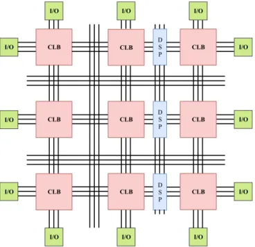
An FPGA is an integrated circuit that can be programmed after manufacturing to function as any digital circuit determined by the designer. The key difference between FPGA and Application Specific Integrated Circuit (ASIC) is that the ASIC can only be used for a cer-tain application. The major building blocks in modern FPGAs consist of Configurable Logic Blocks (CLBs), Interconnections, Input/Output Blocks (IOBs) and embedded blocks such as DSP blocks. An overview of the architecture of modern FPGAs is shown in figure 2.1 [3].
2.1. Field-Programmable Gate Array (FPGA)
CLB D S
P I/O
I/O I/O I/O
I/O
I/O
I/O
I/O I/O I/O
I/O I/O CLB CLB CLB CLB CLB CLB CLB CLB D S P D S P
Figure 2.1: An overview of a typical FPGA architecture. The red boxes indicate a number of CLB blocks distributed over an FPGA. The green boxes indicate input/output blocks of an FPGA. The blue boxes indicate DSP blocks where the focus of this work lies. The vertically and horizontally distributed lines indicate interconnections between the blocks.
2.1.1
Configurable Logic Block (CLB)
The CLB is used to implement logic functions and mathematical operations. Inside each CLB, are so called Configurable Logic Elements (CLEs) which in turn consists of Look-Up Table(LUTs), D-flip flops and a 2-to-1 multiplexers, as illustrated in figure 2.2 [3].
LUT D-flip flop
A B C
Figure 2.2: Simplified internal structure of a typical CLE. The purpose of a LUT is to im-plement mathematical operations such as addition. The LUT box and its three-inputs is de-scribed in figure 2.3
The core of the FPGA consists of thousands of CLE copies connected with each other. The LUT is made of a series of cascaded multiplexers where the LUT inputs are used as the select lines and the inputs to multiplexers is a 1-bit SRAM memory that is set to either 0 or 1. The internal structure of a LUT is shown in figure 2.3 [3].
2.1. Field-Programmable Gate Array (FPGA) 1 0 1 0 1 0 1 0 1 0 1/0 1/0 1/0 1/0 1/0 1/0 1/0 1/0 1 0 A B C 1 0
Figure 2.3: Simplified internal structure of a LUT. The three-inputs of a LUT control the selec-tion of the 1/0 input bit of the multiplexers.
2.1.2
Interconnections
As illustrated in figure 2.1, a big part of the FPGA’s architecture is utilized by vertically and horizontally distributed interconnections. These interconnections consist of switch boxes and connection boxes in order to get the desired connection [3]. Each CLB is surrounded by a group of connection boxes that in turn are connected to each other via a group of switch boxes, as shown in figure 2.4. These connection boxes are used to connect different CLBs to each other and furthermore provide connection to both I/O blocks and embedded blocks [3].
CLB
CB
SB
SB
CB
SB
CB
SB
CB
Figure 2.4: Simplified network of interconnections. SB refers to Switch Boxes and CB refers to Connection Boxes.
2.1. Field-Programmable Gate Array (FPGA)
The placement of interconnections plays an important role in determining the flexibility and efficiency of the FPGA. Therefore, manufacturers nowadays offer flexible construction of in-terconnections including sets of both short and long wires in order to efficiently perform any digital circuit.
2.1.3
Input/Output Block (IOB)
Input/Output blocks are placed all around FPGA’s edges, as shown in figure 2.1 where the IOBs function as a communication interface between the internal signals and the external pins.
2.1.4
DSP Block
Although a Configurable Logic Block is capable of performing arithmetic operations and storing data, it would be too slow and utilizes a huge amount of resources because a CLB is designed to be relatively general in order to perform different types of functions. As the demand for the FPGA is increasing, modern FPGAs offer embedded blocks to perform spe-cific functions, some of which are memory blocks and DSP blocks. The introduction of these embedded blocks clearly reduce area utilization, power consumption and as a consequence results in better performance [2].
Although the internal structure of DSP blocks and its related details are different depending upon manufacturer and device version, the overall architectures of most DSP blocks look alike.
A DSP block consists of an adder and multiplier followed by an accumulator. The aim of introducing DSP blocks are to enhance performance of these arithmetic operations. Also, there are specific connections in each DSP block that can be used to connect multiple DSP blocks to each other which in turn can be used to implement an efficient FIR filter [2].
2.2. Digital Filter
2.2
Digital Filter
A digital filter is used to modify signal characteristics in the time and/or frequency domain. A digital signal is obtained by sampling the continuous signal in different time frames after which the signal is represented as a sequence of discrete values, unlike the analog signal which is continuous and represented as a function of time [10].
Digital FIR filter algorithms can be described mathematically by the difference equation y[n] =
N
ÿ
k´1
ak¨x(n ´ k)or by signal flow graphs that are represented as block diagrams [10].
T
x[n]
x[nk]
y[n]
ak ak
Figure 2.5: An example of a signal flow graph as an alternative representation of the differ-ence equation presented above. The akindicate FIR filter coefficients and x(n ´ k)indicate
delayed versions of input signal x[n].
The fundamental components used in digital filters, as shown in figure 2.5, are multipliers, adders and delay elements. While difference equations are used to describe the relation between the input and output sequence and are therefore an external behavioral of the filter, signal flow graphs are more detailed and are used to exactly compute the output values y[n]
and the internal values in the filter [10].
A Linear time invariant (LTI) filter is one of the most commonly used digital filters. A LTI filter can be described by its impulse response h[n]. Impulse response h[n] is the output obtained by applying an impulse as an input sequence. The output y[n]is obtained by the process of convolution that convolve the impulse response and input sequence in the time domain and can mathematically be presented as y[n] =x[n]¨h[n].
2.2.1
Finite-length Impulse Response (FIR) Filter
LTI filters are usually divided into two types which are finite-length impulse response (FIR) and infinite-length impulse response (IIR). Finite-length impulse response means that the impulse response becomes zero after a finite number of samples. In contrast, the infinite-length impulse response has an infinite number of sample values [10]. The work presented in this thesis covers the FIR filter only.
2.2.1.1 FIR Filter Structures
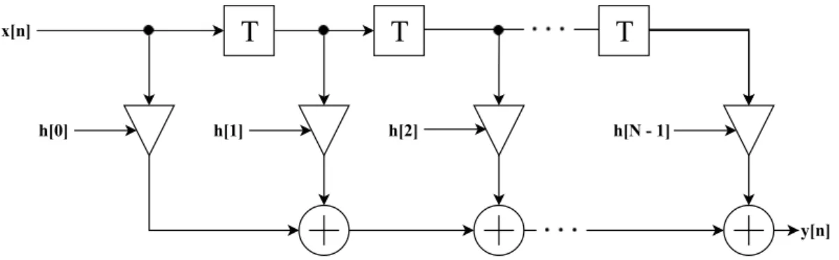
There are different ways to construct FIR filter. Two common ones are classified as 1) direct form structure and 2) transposed direct form structure.
The direct form structure is the classical implementation of the FIR filter equation shown in section 2.2. The input samples are delayed by using delay elements in form of D-flip flops. The direct form structure depends upon so called chain adder where input data is partially computed and outputted through a chain of small adders. The chain adder technique leads to significant reduce in area utilization. The critical path of the FIR filter is the longest path
2.3. Filter Complexity Optimization
of logic between two registers. Latency is the number of inserted pipelined registers between input and output. Figure 2.6 shows the direct form structure of a FIR filter [4].
x[n]
T
h[0] h[1]
T
T
h[2] h[N 1]
y[n]
Figure 2.6: Direct form structure of a FIR filter. x(n)and y(n)are input and output sequence respectively. h[0]. . . h[N ´ 1]represent the coefficients.
The transposed direct form is obtained from the direct form after applying the transposition theorem. Transposition is obtained by replacing inputs with outputs and replacing outputs with inputs where the inputs are directly connected to multipliers [10]. The critical path of transposed structure reduced significantly in comparison with direct form.
T
T
h[0] y[n]T
h[N 1] x[n] h[N 2] h[N 3]Figure 2.7: Transposed direct form structure of the FIR filter where input signals are fed into multipliers directly.
2.3
Filter Complexity Optimization
There are several techniques that are practically used for FIR filter to improve filter imple-mentation by reducing area usage, time and power dissipation.
2.3.1
FIR Filter Symmetry
A FIR filter has the ability to obtain linear phase which in turn implies that the impulse response h(n)presents symmetry where h(n) = h(N ´ n) where N is the filter order and x[n]are the input samples. Figure 2.8 shows the impulse response of 9 coefficients FIR filter where figure 2.9 and figure 2.10 show the representation of an odd number FIR filter in signal flow graph in direct form and transposed direct form respectively.
The math behind resource reduction when using symmetry follows the distributive property of multiplication as illustrated in the following example:(x ¨ y) + (x ¨ z) =x(y+z)while the left hand side of the equation performs two multiplications and one addition, the right hand side performs only one multiplication and one addition [1].
2.3. Filter Complexity Optimization h[0] h[1] h[2] h[3] h[4] h[5] h[6] h[7] h[8]
Figure 2.8: Impulse response of 9-tap linear phase FIR filter.
The implementation of impulse response symmetry in figure 2.8 can be shown in figure 2.9 where the input delay chain is fed forward and backward to save resources. Two symmetric coefficients are now represented with a single multiplier.
T
T
h[(N 1)/2] h[0] x[n] h[1]T
T
T
T
y[n]Figure 2.9: Symmetric FIR filter structure in direct form. Each multiplier represent two coef-ficients and therefore the total usage of multipliers are decreased to half.
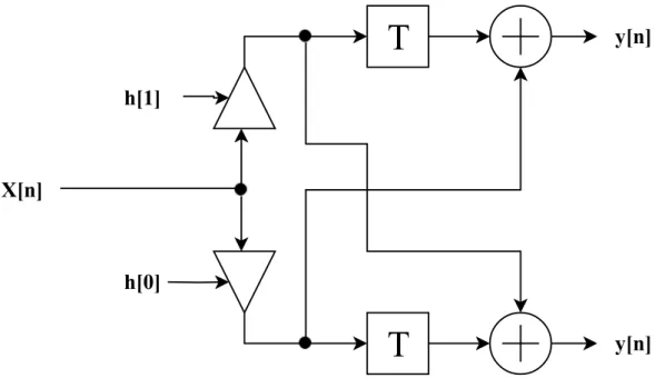
The impulse response symmetry can also be implemented in transposed direct form where the total usage of multipliers are decreased to half, as shown in figure 2.10.
T
y[n]T
h[N 1] x[n]T
h[N 2]Figure 2.10: Symmetric FIR filter structure in transposed direct form. Each multiplier repre-sent two coefficients and therefore the total usage of multipliers are decreased to half. The dashdotted box indicates one Look-Up table.
2.3. Filter Complexity Optimization
2.3.2
Input sharing of Multiple FIR filters
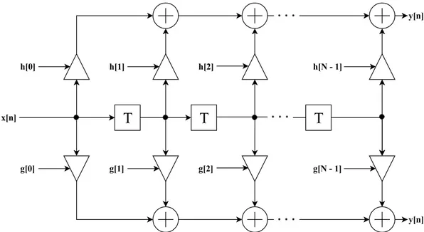
The input sharing of multiple FIR filters are beneficial when dealing with large numbers of filters because of its ability to save area. The input sharing of the direct form FIR filter can be shown in figure 2.11 where the delay element is shared between two filters.
x[n]
T
T
T
y[n] g[0] h[0] g[1] h[1] g[2] h[2] g[N 1] h[N 1] y[n]Figure 2.11: Input Sharing of two FIR filters h and g in direct form. Input delay element is shared between the filters h and g to save resource usage.
The input sharing can also be used in transposed direct form, however, it would not be bene-ficial in saving area when using non-symmetric coefficients because of no resources are going to be shared.
2.3.3
Interpolation
The interpolation process is a multi-rate filter technique used to increase sample rate or sample frequency in order to obtain a certain function.
The reduction in memory and computation time is obtained by so called polyphase interpo-lator where the interpolation process is divided into multiple stages. The input signal x[n]
is fed through the polyphase interpolator which consist of subfilters placed in parallel. Af-terwards, each subfilter outputs the corresponding input sample and send it to output y[n]
through a commutator, as shown in figure 2.12 [4].
h0[n] h1[n] h2[n]
hp1[n]
x[n] y[n]
Figure 2.12: The concept of polyphase interpolator. The input x[n]feds into subfilters and sent to output y[n].
2.3. Filter Complexity Optimization
2.3.3.1 Exploiting Symmetry in Polyphase Interpolator FIR Filter
As described in subsection 2.3.3, a polyphase interpolator divides the symmetric coefficients of interpolation filter into subfilters. The subfilters can be symmetrical or non-symmetrical. When the coefficients of the subfilters are symmetrical (as for linear phase), the transposed direct form structure can be obtained as shown in figure 2.13.
T
h[0]
X[n]
h[1]
T
y[n]
y[n]
Figure 2.13: Symmetric coefficients of two FIR filters in transposed direct form. However, the coefficients of subfilters are not necessarily symmetric in themselves. There-fore, a technique called symmetric pairs is performed to obtain symmetry when coefficients of subfilters are not symmetric [4]. The number of subfilters is determined by the factor L. For simplicity, the following example demonstrates the symmetric pairs technique for a 12 coefficients interpolated filter by factor 3. The filter coefficients in the example below can be seen as impulse response in figure 2.8 but with 12 coefficients instead of 9 coefficients. The filter coefficients 1, 2, 3, 4, 5, 6, 6, 5, 4, 3, 2, 1 produce the following subfilters: H1=1 , 4 , 6 , 3H2=2 , 5 , 5 , 2 H3=3 , 6 , 4 , 1
The example above shows that the subfilter H2 is symmetric while the other two filters, H1 and H3 are non-symmetric. By using the symmetric pairs technique, new subfilters produced where:
H1=1+3 , 4+6 , 6+4 , 3+1= 4 , 10 , 10 , 4 H2=2, 5, 5, 2
H3=3 ´ 1 , 6 ´ 4 , 4 ´ 6 , 1 ´ 3=2 , 2 , ´2 , ´2
Symmetry are now obtained in H1 and H3, although H3 has a negative symmetry, and the area reduction is satisfied according to symmetry features discussed earlier.
3
Method
In order to study how FIR filter is mapped on Xilinx FPGAs, the process is divided into several stages.
The first stage is to determine the DSP slice versions that will be studied and they are DSP48E for FPGA Virtex-5, DSP48E1 for 6- and 7-series FPGAs and DSP48E2 for Ultrasclae FPGA. Afterwards, the data sheets of corresponding DSP slice version are studied and an overview are taken of each DSP slice version.
The second stage is to focus on the unique features in each DSP version that are specifically designed for the implementation of the FIR filter. The focus is to determine the features of a certain DSP slice which is not found in the other DSP versions. Afterwards, different types of filter structures are studied were each filter structure is mapped in a different way. The focus is on presenting a cost model in form of utilized DSP slices and then determine the latency of the corresponding structure. The utilized DSP slices and clock cycles latency are calculated separately.
The third stage is the simulation of various types of FIR filter structures on the coefficients generator and then comparing the results obtained from the generator with those found in corresponding data sheets. The generator used for coefficients generating is Xilinx CORE Generator version 5.0 for the Virtex-5 DSP48E and version 6.3 for the 7-series DSP48E1 and UltraSclae DSP48E2.
The Xilinx CORE Generator software is used for generating coefficients of just single FIR filter because the input-share feature is not supported by the software. In addition, the symmetry of transposed structure is not supported either.
4
Results
The results presented in this chapter are divided as follows:
The features of the three DSP slice types are presented. Afterwards, different FIR filter struc-tures and their resource utilization are presented for single FIR filter. The last section in this chapter presents the different FIR filter structures and the associated resource utilization when multiple FIR filters share the input signal.
4.1
Features of The DSP Slice Types
Xilinx first introduction of the DSP48 slice architecture is though to deliver programmable devices with more flexibility and higher capability of performing logic operations and im-plementing digital signal processing applications. The three DSP slice types discussed below are considered an improvement of the DSP48 slice version while the features of the presented DSP slice types have a lot of similarities but also important differences. The main differences are discussed below.
4.1.1
Virtex-5 FPGA DSP48E Slice
The DSP48E slice is an extension of the DSP48 slice as mentioned above. The DSP48E comes with all the features introduced in the DSP48 and even more. One of the important features included in DSP48E is the 25 ˆ 18 complement multiplier instead of 18 ˆ 18 two’s-complement multiplier offered in DSP48 [12]. The DSP48E has no pre-adder.
4.1. Features of The DSP Slice Types
T
T
T
T
T
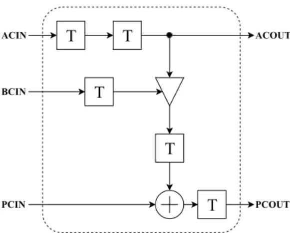
BCIN PCIN PCOUT ACIN ACOUTFigure 4.1: Simplified schematic of a DSP48E slice. ACI N, BCI N and PCI N are the only inputs to the slice while ACOUT and PCOUT are the only outputs. The dashed box indicates a closed DSP slice block where it is prohibited to reach any desired signal inside this block.
The add and subtract feature in DSP48 is extended to even handle logic operations in DSP48E. The DSP48E has a cascade path ACI N, BCI N and PCI N in form of input paths and ACOUT and PCOUT as an output paths. The input and output paths are used to cascade multiple DSP slices with each other and resulting in so-called cascaded chain [12].
It should be mentioned that the DSP48E include more improvements, but they are less im-portant in this work.
4.1.2
The 7-Series FPGA DSP48E1 Slice
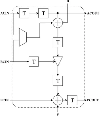
The Xilinx 7-series FPGA DSP48E1 slice fundamental resources consist of 25 ˆ 18 two’s- com-plement multiplier, 48-bit accumulator and a 25-bit pre-adder. The pre-adder contribute in reducing the number of utilized resources and thereby leads to low power consumption when symmetrical coefficients are used [13]. The pre-adder has a 25-bit input vector D. The pur-pose of the input vector D is to increase capacity of the ACI N path. The presence of input, output and intermediate pipelined registers also serve in increasing throughput. Figure 4.2 shows an overview of a DSP48E1 slice architecture.
T T T BCIN PCIN PCOUT T T ACIN ACOUT T D
Figure 4.2: Simplified schematic of a DSP48E1 slice. ACI N, BCI N, PCI N and D are the only inputs to the slice while ACOUT and PCOUT are the only outputs. The dashed box indicates a closed DSP slice block where it is prohibited to reach any desired signal inside this block.
4.1. Features of The DSP Slice Types
4.1.3
UltraScale FPGA DSP48E2 Slice
The DSP48E2 slice is an improved version of the DSP48E1 discussed in subsection 4.1.2. The main improvements include optimizing the 25 ˆ 18 two’s complement multiplier to a 27 ˆ 18 two’s complement multiplier, 27-bit pre-adder instead of 25-bit pre-adder in DSP48E1. The pre-adder has a 27-bit input vector D. The pre-adder has more flexibility by selecting inputs from the input paths ACI N or BCI N. The adder capability is increased by introducing a third input operand F instead of two-input adder in DSP48E1 [14]. Figure 4.3 shows an overview of a DSP48E2 slice architecture.
T
T
T
BCIN PCIN PCOUTT
T
ACIN ACOUTT
D FFigure 4.3: Simplified schematic of a DSP48E2 slice. ACI N, BCI N, PCI N, D and F are the only inputs to the slice while ACOUT and PCOUT are the only outputs. The dashed box indicates a closed DSP slice block where it is prohibited to reach any desired signal inside this block.
4.2. FIR Filter Structures and Resource Utilization
4.2
FIR Filter Structures and Resource Utilization
The resource utilization is dependent upon the FIR filter structure, as discussed below.
4.2.1
Pipelined Direct Form FIR Filter
The pipelined direct form FIR filter structure in DSP48E, DSP48E1 and DSP48E2 looks alike with respect to area utilization. However, they have different latency.
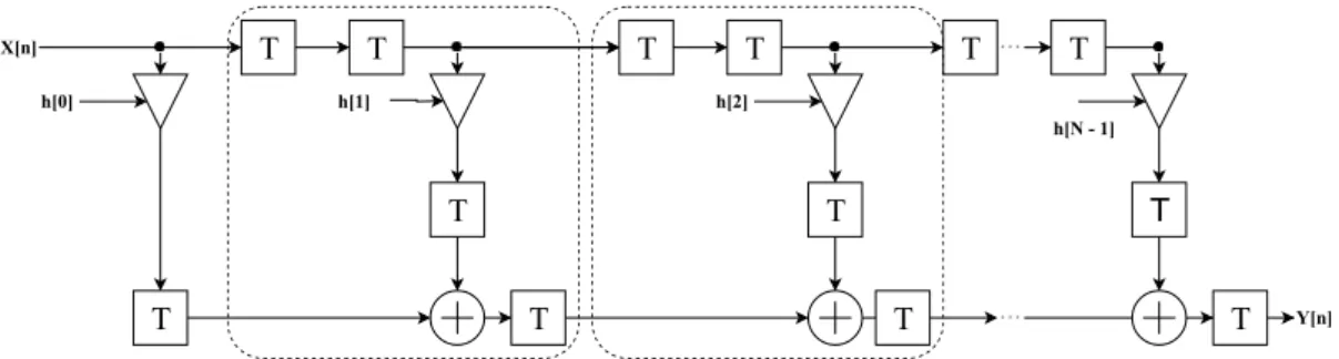
One of the most important characteristics of DSP48E slice, as well as DSP48E1 and DSP48E2 is its ability to cascade multiple DSP slices to shape certain functions such as a FIR filter. The cascade function is performed by connecting multiple adders in series. The cascade-addition is applied by connecting the input and the output of one DSP slice to the neighbour DSP slice resulting in higher performance and reduction in utilized resources because the logic outside DSP slice blocks is not used. The minimal use of the FPGA-logic gives better efficiency and less resource utilization [4]. Figure 4.4 shows the structure of the direct form FIR filter structure for the slice types DSP48E, DSP48E1 and DSP48E2.
Y[n] X[n] T T T T T h[0] h[N 1] T h[1] T T T h[2] T T T T
Figure 4.4: Non-symmetric direct form FIR filter structure in DSP48E, DSP48E1 and DSP48E2 where the area marked in dashed box indicates one DSP slice.
The direct form FIR filter structure in DSP48E, DSP48E1 and DSP48E2 utilize N DSP slice/block for N non-symmetric coefficients.
The initial latency for the slice DSP48E is 5+N clock cycles[12], while the initial latency for the slice DSP48E1 is 6+N [13] and an initial latency of 6+N clock cycles for the slice DSP48E2 [14].
4.2.2
Symmetric Pipelined Direct Form FIR Filter
The direct form FIR filter gives the opportunity to use coefficient symmetry to minimize the required DSP slices without affecting the functionality and speed. By taking advantage of the pre-adder, the symmetric pipelined direct form FIR filter requires N/2 DSP slice for N coefficients. However, symmetric pipelined direct form FIR filter makes use of logic outside DSP blocks, in the FPGA.
The utilized logic in DSP48E depends upon input bit width W and coefficients N where the utilized DSP slices is((W+1)¨(N/2)) + (W/2). The initial latency is 6+N clock cycles [11]. Figure 4.5 shows the symmetric pipelined direct form FIR filter structure in DSP48E.
4.2. FIR Filter Structures and Resource Utilization
T
T
T
T
T
T
T
T
h[1]T
T
T
T
T
T
h[(N 1)/2]T
T
T
T
T
h[0] y[n] x[n]Figure 4.5: Symmetric pipelined direct form FIR filter structure in DSP48E where the dashed box indicates one DSP slice and the dashdotted box indicates one LUT.
The resource utilization in DSP48E1 is the same as DSP48E with respect to the number of utilized DSP slices, i.e. N/2 DSP slice. However, the Look-UP table logic utilization is way less than DSP48E, as illustrated in figure 4.6. The utilized logic in DSP48E1 is[N/16]LUTs and the initial latency is 7+N where one DSP slice takes 8 clock cycles, two DSP slices take 9 clock cycles, and so on [13].
T T T T h[0] y[n] T x[n] T T T T T T T T T T T T T T T T h[1] T T T T T T T T h[(N 1)/2]
Figure 4.6: Symmetric pipelined direct form FIR filter structure in DSP48E1 where the dashed box indicates one DSP slice and the dashdotted box indicates one LUT.
The resource utilization in DSP48E2 is the same as DSP48E1 with respect to the number of utilized DSP slices and logic, i.e. N/2 DSP slice+[N/16]LUTs.
4.3. Generated Results
4.2.3
Transposed Direct FIR Filter
The transposed direct FIR filter utilize N DSP slices for N non-symmetric coefficients for DSP48E, DSP48E1 and DSP48E2. However, the three DSP slice types have different latency. The DSP48E and DSP48E2 have a constant latency of 6 clock cycles whereas the transposed direct form FIR filter structure in DSP48E1 has a constant latency of 8 clock cycles. Figure 4.7 shows the FIR filter structure of a transposed direct form in DSP48E, DSP48E1 and DSP48E2.
T T T T T T T T h[0] Y[n] T T T T 0 h[N 1] X[n] h[N 2]
Figure 4.7: Transposed direct form FIR filter structure in DSP48E, DSP48E1 and DSP48E2.
4.2.4
Transposed Symmetric FIR Filter
The transposed symmetric FIR filter utilize N/2 slices for N non-symmetric coefficients for DSP48E, DSP48E1 and DSP48E2. However, they have different latency. The DSP48E and DSP48E2 have a constant latency of 6 clock cycles where the transposed symmetric form FIR filter structure in DSP48E1 has a constant latency of 8 clock cycles. Figure 4.8 shows the FIR filter structure of a transposed direct form in DSP48E, DSP48E1 and DSP48E2.
T
y[n]T
h[N 1] x[n]T
h[N 2]Figure 4.8: Transposed symmetric form FIR filter structure in DSP48E, DSP48E1 and DSP48E2 where a dash box indicates one DSP slice and a dashdotted box indicates one LUT.
4.3
Generated Results
The following table shows the generated results of the utilized resources of single FIR fil-ter in DSP48E, DSP48E1 and DSP48E2. The generation of coefficients is run by using Core Generator software tool by Xilinx.
4.4. Input Sharing of Multiple FIR Filters
Filter Structure DSP Slice Type DSP Slices Latency LUTs
Non-symmetric direct DSP48E N 5+N None
Non-symmetric direct DS48E1 N 6+N None
Non-symmetric direct DS48E2 N 6+N None
Symmetric direct DSP48E N/2 6+N (W+1)ˆ(N/2) + (W/2)
Symmetric direct DSP48E1 N/2 7+N N/16
Symmetric direct DSP48E2 N/2 6+N N/16
Transposed direct DSP48E N 6 None
Transposed direct DSP48E1 N 8 None
Transposed direct DSP48E2 N 6 None
Symmetric transposed DSP48E N/2 6 W ˆ N
Symmetric transposed DSP48E1 N/2 7 N
Symmetric transposed DSP48E2 N/2 6 N
Table 4.1: Simulated results of utilized resources of single N-tap FIR filter in DSP48E, DSP48E1 and DSP48E2.
4.4
Input Sharing of Multiple FIR Filters
The results presented in the table above present the resource utilization of the three DSP slice types DSP48E, DSP48E1 and DSP48E2 with respect to a single FIR filter. The results presented in the following sections belong to the input sharing of multiple FIR filters.
4.4.1
Input Sharing of Pipelined Direct Form FIR Filter
Input sharing of K FIR filter in DSP48E, DSP48E1 and DSP48E2 gives K ˆ N DSP slices for N non-symmetric coefficients. Figure 4.9 illustrates input sharing of two FIR filters in pipelined direct form. The initial latency is the same for respective type of DSP slice as discussed in the single FIR filter in subsection 4.2.1.
X[n] T T T g[0] T T T T T T T T T T h[0] T T T T T h[1] g[1] g[2] Y[n] T T T h[N 1] T T T Y[n] T T h[N 1] h[2]
Figure 4.9: Input sharing of two FIR filters in pipelined direct form. No resource reduction is obtained because the resources are not shared between the two filters.
4.4. Input Sharing of Multiple FIR Filters
4.4.2
Input Sharing of Symmetric Pipelined Direct Form FIR Filter
Unlike FIR filter structures in non-symmetric direct and transposed form, the symmetric pipelined direct form FIR filter structure utilizes LUTs logic which in turn can be used in input sharing.
In DSP48E symmetric FIR filter, LUT logic usage is preferred more than a DSP slice. The data is pre-added before the multiplication with the coefficients. The introduction of chain input delay buffer saves logic by using an SRL16E shift register [11]. The adder chain is reduced by half due to symmetry which in turn leads to reduction in latency. Figure 4.10 shows the structure of two symmetric pipelined direct form FIR filter in DSP48E.
T
T
T
T
T
T
T
T
h[1]T
T
T
T
T
T
h[(N 1)/2]T
h[0] y[n] x[n]T
T
T
T
g[1]T
T
T
T
g[0]T
T
T
T
y[n] g[(N 1)/2]T
T
T
T
Figure 4.10: Input sharing of two symmetric direct FIR filter in DSP48E. Input delay buffer and pre-adder are shared between the filters g and h.
In DSP48E1 and DSP48E2, the initial latency for respective DSP types still the same as men-tioned in the single FIR filter. However, the input sharing of multiple filters give logic utiliza-tion of[N/16]LUTs. The figure 4.11 illustrate input sharing of 2 symmetric direct FIR filters in DSP48E1 as well as DSP48E2.
4.4. Input Sharing of Multiple FIR Filters T T T T g[0] y[n] T x[n] T T T T T T T T T T T T T T T T g[1] T T T T T T T T g[(N 1)/2] T T T T T T T h[0] T T T T T T T h[1] T T T T T T T h[(N 1)/2] y[n]
Figure 4.11: Input sharing of two symmetric direct FIR filters in DSP48E1 and DSP48E2. Input buffer delay is shared between the filters g and h.
4.4.3
Input Sharing of Transposed FIR filter
Input sharing of K FIR filter in DSP48E, DSP48E1 and DSP48E2 gives K ˆ N DSP slices for N non-symmetric coefficients as illustrated in figure 4.12. The initial latency is the same for respective type of DSP slice as discussed in the single FIR filter.
X[n] T T T T h[0] T T h[N 1] T g[0] T T g[N 1] T T T T T T T T Y[n] T 0 g[N 2] T T T h[N 2] T T Y[n] T 0
Figure 4.12: Input sharing of two FIR filters in transposed direct form. No resource reduction is obtained because the resources are not shared between the filters g and h.
4.5. Generated Results
4.4.4
Exploiting Symmetry in Polyphase Interpolator FIR Filter
The symmetric pairs technique is obtained by adding and subtracting the output of subfilters H1 and H3, as discussed in section 2.3.3 . Afterwards, the subfilters H1 and H3 are scaled by a factor of a hal f to obtain the output of the primary filter, as illustrated in figure 4.13.
x[n] y[3n] h1[n] h2[n] h3[n] 1/2 1/2 y[3n+1] y[3n+2]
Figure 4.13: Symmetric pairs technique of 12 coefficients interpolated by 3 polyphase subfil-ters.
The symmetric pairs technique can be applied when using an even number of coefficients interpolated by 2, for example: H=1, 2, 3, 3, 2, 1 introducing subfilters H1=1, 3, 2 and H2=
2, 3, 1. The subfilters are not symmetric in themselves, therefore symmetric pairs technique is needed to obtain symmetry. However this technique is not required when the number of coefficients is odd and interpolated by 2, for example: H = 1, 2, 3, 4, 3, 2, 1 introducing subfilters H1 = 1, 3, 3, 1 and H2 = 2, 4, 2 do not need symmetric pairs technique because filter symmetry is already satisfied. By using the symmetric pairs technique, N coefficients take N/2 DSP slices, as in normal symmetry, and N DSP slices otherwise.
4.5
Generated Results
The following table shows the generated results of the utilized resources of K parallel N-tap FIR filter in DSP48E, DSP48E1 and DSP48E2. The generation of coefficients is run by using Core Generator software tool by Xilinx.
Filter Structure DSP Slice Type DSP Slice Latency LUTs
Non-symmetric direct DSP48E K ˆ N 5+N None
Non-symmetric direct DS48E1 K ˆ N 6+N None
Non-symmetric direct DS48E2 K ˆ N 6+N None
Symmetric direct DSP48E K ˆ(N/2) 6+N (W+1)ˆ(N/2) + (W/2)
Symmetric direct DSP48E1 K ˆ(N/2) 7+N N/16
Symmetric direct DSP48E2 K ˆ(N/2) 6+N N/16
Transposed direct DSP48E K ˆ N 6 None
Transposed direct DSP48E1 K ˆ N 8 None
Transposed direct DSP48E2 K ˆ N 6 None
Symmetric transposed DSP48E K ˆ(N/2) 6 N ˆ W
Symmetric transposed DSP48E1 K ˆ(N/2) 7 N
Symmetric transposed DSP48E2 K ˆ(N/2) 6 N
Interpolator non-symmetric direct DSP48E K ˆ N 5+N N Interpolator symmetric transposed DSP48E1 K ˆ(N/2) 7+N N
Interpolator symmetric pairs DSP48E2 K ˆ N 6+N K ˆ(N/2)
Table 4.2: Simulated results of utilized resources of K parallel N-tap FIR filters in DSP48E, DSP48E1 and DSP48E2.
The generated results presented above applies to all Filter structures in table 4.2 where the number of filters are k parallel N-tap FIR filter.
5
Discussion
In this section, the results obtained will be discussed and analyzed as well as the methodology used in this work. Finally, the work is going to be seen in a wider perspective where the ethical and environmental effects of the manufacturing process of electronics are discussed.
5.1
ASIC vs FPGA
When designing a system, it is of importance to decide in advance which integrated circuit is going to be used. ASIC and FPGA based circuits have many characteristics in common, but also many differences. A brief introduction of the most common differences will be presented below.
5.1.1
Benefits of an ASIC Based Circuit
One of the most important aspects when designing a system is its performance. ASIC pro-vides approximately 3.2 higher performance than the FPGA according to a comparison study of more than 20 different designs [2].
Another benefit of using ASIC instead of FPGA is the low power consumption associated with ASIC based systems. An FPGA contains a lot of logic in order to cover the implemen-tation of different functions, which in turn lead to more power consumption than an ASIC based design. Although FPGA designs aimed for low power consumption customers exist, most are not. [2].
Conceptually, the most important feature offered by an ASIC based design and what makes it more preferable than an FPGA based design is its flexibility. In spite of the fact that the modern FPGAs contain dedicated blocks, these blocks are designed to be very general in order to perform many different functions. The drawback of having blocks for general use make the FPGA less desired for many users. In contrast, an ASIC can be designed by a user to implement any circuit as well as implementing self-specialized blocks for the desired application [2].
5.2. Results
5.1.2
Benefits of an FPGA Based Circuit
In addition to ASIC, An FPGA also contains considerable advantages. An FPGA can be useful when designing a prototype where test and evaluation process can be performed on parts of the design, even when the design is not fully completed [2]. In contrast, manufacturing parts of an ASIC will be expensive.
The low cost of the FPGA device makes it available even for hobbyists to start using the FPGA. In contrast, the tool cost for ASIC is much more than the FPGA and can therefore not be affordable by many users.
An FPGA provides configurability through the big amount of embedded logic. The logic can be used to design any desired circuit. However, the availability of logic lead to that some of the logic will not be used which in turn can lead to lower performance and high power consumption compared to an ASIC design. The self-configurability feature in an FPGA can help the designer to keep the design private and not hand it over to an outside party. This feature gains more interest when dealing with designs that contain confidential information such as cryptographic codes [2].
5.2
Results
The results are going to be discussed in the following sections.
5.2.1
Pipelined Direct Form vs Transposed Direct form
The results presented for single FIR filter and input sharing of FIR filter show that the utilized DSP slices for mapping a FIR filter on FPGA is the same for direct and transposed direct form FIR filter structure. However, they have different clock cycle latency. Another factor that might be of interest in analyzing the direct and transposed structure are their throughput. In transposed structure, the input chain sends data from the input to the output with no delay element in-between which in turn can lead to speed challenges. However, the latency of direct form FIR filter increases by increasing filter taps (as shown in table 4.1) while the latency in transposed direct form is constant.
As the focus of this work is primarily on resource utilization, the transposed form structure is still preferred when the number of utilized DSP slices for mapping a FIR filter on FPGA is the same as in the corresponding direct form structure. It should be noted that both direct and transposed structures do not use Look-Up table logic in the implementation of the FIR filter which in turn saves a lot of resources.
5.2.2
Resource Utilization in Direct Form DSP48E vs. DSP48E1 and DSP48E2
When dealing with symmetric coefficients in pipelined direct form structure, the latency in the three DSP slice types have approximately the same latency. However, it is of importance to shed light on resource utilization differences between DSP48E on one hand, DSP48E1 and DSP48E2 on the other hand.
Although symmetric coefficients utilize the same amount of DSP slices in all three structures, the utilized LUT logic is different. Symmetric pipelined direct form FIR filter in DSP48E slice, as shown in figure 4.5, implement the chain input as well as the adder in the LUT logic which in turn lead to significant resource utilization and power dissipation. In contrast to DSP48E and as the use of symmetric coefficients increased by users, symmetric pipelined direct form FIR filter in DSP48E1 and DSP48E2 have traded-off DSP slices (as shown in figure 4.6) by inserting the pre-adder and the chain input delay into the DSP slice while the logic has been
5.3. Method
changed from the LUTs as an operation mode into SRL16E. The 16-bit shift register SRL16E is used to improve performance and area efficiency.
5.2.3
Input Sharing in FIR Filter with ASIC Perspective
In the single FIR filter, mapping a DSP slice into FPGA is considered beneficial by efficient utilization of the area. However the implementation of input sharing FIR filter can be less effective in some cases.
In figure 4.9 as an example, input sharing of two pipelined direct form FIR filters is shown. Each DSP slice can be thought of as a closed box where it is prohibited to reach the signals inside this box. By assuming that the two pipelined direct form FIR filter are replaced by a ten FIR filter of the same type, it would be less practical to use the direct form structure as the delay elements of the shared input can not be used to reduce area utilization. In contrast to FPGA, ASIC can be used to implement the two pipelined direct form FIR filter shown in figure 4.9 as illustrated in figure 5.1 where the input delay chain is shared between the two filters resulting in effective utilization of resources.
X[n]
T
T
g[0] h[0] g[1] h[1]T
y[n]T
y[n]Figure 5.1: Mapping of two pipelined direct form FIR filter in ASIC.
Symmetry in pipelined direct form FIR filter, as shown in figures 4.10 and 4.11, use LUTs logic in addition to DSP slices. In parallel implementation of a FIR filter, the input sharing is practical because of the savings of resources. However, the DSP slices in DSP48E on one hand, DSP48E1 and DSP48E2 on the other hand use logic differently. As it is preferred to use the DSP48E1 and DSP48E2 approach in single FIR filter as discussed earlier, it is obvious that the approach might not be as good when using many filters in parallel. Therefore, the more number of a FIR filter the better it is to not use the built-in registers in order to save power. Symmetry in transposed direct FIR filter is not included in Xilinx Core Generator. However, the symmetry of transposed FIR filter in ASIC can be obtained as shown in section 2.3.1.
5.3
Method
Traditionally, the FIR filter structures are viewed as adders, multipliers and delay elements that are connected in series when they are mapped in hardware. This is partially true but not the wholly true because the target device in implementing the FIR filter determines the view of how to look at the structure.
In ASIC, FIR filter resources are counted as adders, multipliers and delay elements. In con-trast, the counting of FPGA is done by determining the number of DSP slices and Look-Up
5.4. Ethics of Manufacturing Companies
tables. As discussed earlier, there are difference in calculating resources as adders, multi-pliers and delay elements than calculating DSP slices. The reason is that an ASIC based design offers more flexibility in reaching the required signal and thus designing the desired application while it is not the case for an FPGA because of the pre-construction of the DSP slices by the FPGA manufacturer.
FIR filter structures generator Core Generator by Xilinx does have some limitations such as missing an option of utilizing symmetry in transposed direct form as well as sharing input of several FIR filter structures. Efforts has been made to think individually how it would looks like using symmetry in this case. Taking the transposed direct structure in figure 2.6 as an example, the filter symmetry can be obtained by implementing the adder chain placed in the bottom of the structure in the LUTs logic instead of DSP slice.
The work presented in this thesis has some deficiency. There is a factor of difference in clock cycle latency between the generator results and the data sheets of the three DSP slice types that the author has not figured out the reason behind. If the number of clock cycle latency in generator results has matched the corresponding latency in data sheets, the results would have presented clearly and precisely.
It should also be mentioned that this work does not contain all the possible scenarios that could affect the resource utilization in implementing the FIR filter, such as decimation of the FIR filter.
As long as the target device manufacturer is Xilinx and the results are taken from the genera-tor created by the same manufacturer, the results provide high quality and should be consid-ered reliable. Thus, the results would be the same if this work is done again using the same methodology discussed in this work.
5.4
Ethics of Manufacturing Companies
Since the arise of the technology in the late 1980’s the world has changed dramatically, and technology is so dominant in our daily lives. Electronics and more specifically integrated cir-cuits such as FPGAs have played a key role in creating and developing systems and allowing more people to engage in technology. In order to understand the process of manufactur-ing electronics, a closer look is taken to analyze how electronic manufacturmanufactur-ing companies produce products and how they handle ethical issues. The analysis process is based on as-sessment schedule made by [5] and the precautionary principle.
5.4.1
Assessment Schedule
There are many stakeholders in a manufacturing company including customers, suppliers and owners that play an important role in driving a company. It is obvious that most of the time the customers need a functionable products that serve their needs, no matter how environment-friendly the products are, and at the same scale, almost all owners care only about how much money they can make. The relation between the company’s behavior and customers’ needs can be changed by raising awareness among customers about the impor-tance of taking a part by forcing the companies to change their morals and conditions so that it matches customers’ needs and not exposing them into danger by using such products. A similar example would be when the car manufacturer Volkswagen cheated in gas ex-hausters by manipulating software to read false data than the actual tests would give. When people figured out Volkswagen’s cheat, they stopped using these cars and the company had to change their strategy by introducing better cars. According to utilitarianism, the producing
5.5. Source Criticism
of electronic circuits benefit the majority of people that use these products and therefore they do not care about small consequences. Unlike utilitarianism, the deontological ethics con-sider the act instead of the consequences. For instance, an employee follows their boss orders because it is his duty to do so. New solutions could be presented, such as making strict regu-lations on extraction of raw materials, increasing rates on non-environmental power sources. It is applicable if there are political willpower [5].
5.4.2
Precautionary Principle
Precautionary principle based on scientific certainty is crucial and all companies should there-fore take it into consideration to benefit the whole society, for instance if we take it from power consumption point of view, we can efficiently consume power and it would lead to reducing greenhouse effects. Regulations on scientifically proven high quality raw materials and the use of them lead to reducing of bad consequences that would harm humans and so-ciety. These raw materials would be cleaner and environment friendly when recycling them. Strong precautionary principle also applies on security issues in form of insulting human rights, disease causing and integrity insulting by selling products that is not fully safe and not mentioning the bad consequences that could possibly happen [5].
5.5
Source Criticism
The sources used in this work is a combination of books, datasheets and Ph.D. theses. The book authored by Hakan Johansson and Lars Wanhammar [10] at Linkoping university is published in 2011. Hakan Johansson is a professor that works in Linkoping university and has authored several books that discuss linear systems, digital filters and more. Thus, the source [10] should be reliable. The source [5] is written by Sven Ove Hansson who is a professor in philosophy in Royal Institute of Technology (KTH) in Stockholm. The book is published in 2008 and considered new. Hansson has published approximately 30 books in relative areas to the one used in this work. The KTH reputation and the author position gives him trustworthiness. The use of the articles [9], [6] and [7] are taken from IEEE website which is the world’s largest professional organisation in technology and electronics field. Furthermore, the source [7] has been cited by three other papers which gives it validity. Ph.D. theses have also been used. They were done in well-know universities in the world and are relatively new which are considered a positive sign.
The majority of information in this work comes from the official data sheets and white papers presented by Xilinx. The data sheets of DSP slice types are well-known in industry and comes from Xilinx which itself invented the FPGA circuit.
6
Conclusion
It has been shown that the different types of DSP slices have different features that are spe-cially designed for FIR filter implementation. The utilized resources are different according to filter structures which lead to different trade-offs between area, speed and power dissipa-tion.
FPGA based system designs and ASIC based system designs are two two different systems. There is a common misconception between users when dealing with these two different sys-tems. The resources of an FPGA are DSP slice-based where each DSP slice is considered a closed block where its internal signals are unreachable. In contrast, ASIC resources consist of adders, multipliers and delay elements. Access on ASIC signals can be reached almost anywhere in the circuit
6.1
Future Work
According to the limited time that is set for this work to be done, this thesis discussed only one manufacturer. It would be of interest to cover more manufacturers in order to determine which manufacturer’s approach implement the most effective FIR filter with respect to the scenarios presented in this work.
Bibliography
[1] Matthew John Dallmeyer. “Reducing FIR Filter Costs: A Review of Approaches as Ap-plied to Massive Fir Filter Arrays”. PhD thesis. University of Dayton, 2014.
[2] Andreas Ehliar. “Performance driven FPGA design with an ASIC perspective”. PhD thesis. Linköping University Electronic Press, 2009.
[3] Umer Farooq, Zied Marrakchi, and Habib Mehrez. “FPGA architectures: An overview”. In: Tree-based Heterogeneous FPGA Architectures. Springer, 2012, pp. 7–48.
[4] LogiCORE IP Product Guide. “FIR Compiler v7.2”. In: ().
[5] Sven Ove Hansson and Kalle Grill. Teknik och etik. KTH: s filosofienhet, 2008.
[6] Mahesh Kadam, Kishor Sawarkar, and Sudhakar Mande. “Investigation of suitable DSP architecture for efficient FPGA implementation of FIR filter”. In: Communication, Information & Computing Technology (ICCICT), 2015 International Conference on. IEEE. 2015, pp. 1–4.
[7] Ying Li, Chungan Peng, Dunshan Yu, and Xing Zhang. “The implementation methods of high speed FIR filter on FPGA”. In: Solid-State and Integrated-Circuit Technology, 2008. ICSICT 2008. 9th International Conference on. IEEE. 2008, pp. 2216–2219.
[8] Uwe Meyer-Baese and U Meyer-Baese. Digital signal processing with field programmable gate arrays. Vol. 2. Springer, 2004.
[9] J Selvakumar, Vidhyacharan Bhaskar, and S Narendran. “FPGA based efficient fast FIR algorithm for higher order digital FIR filter”. In: Electronic System Design (ISED), 2012 International Symposium on. IEEE. 2012, pp. 43–47.
[10] Lars Wanhammar and Håkan Johansson. Digital filters using Matlab. Department of Electrical Engineering, Linköping University, 2011.
[11] UG073 Xilinx. XtremeDSP for Virtex-4 FPGAs User Guide. 2007. [12] UG193 Xilinx. Virtex-5 FPGA XtremeDSP Design Considerations. 2017. [13] UG479 Xilinx. 7 Series DSP48E1 Slice User Guide. 2018.