Structure-dependent charge transfer at the interface between organic thin
films, and metals and metal oxides
Sareh Ahmadi
Doctoral Thesis in Microelectronics and Applied Physics
Stockholm, Sweden 2013
KTH Royal Institute of Technology ISBN 978-91-7501-934-5 School of Information and TRITA-ICT/MAP AVH Report 2013: 06 Communication Technology ISSN 1653-7610 SE-164 40 Kista ISRN KTH/ICT/-MAP/AVH-2013:06-SE SWEDEN
Akademisk avhandling som med tillstånd av Kungl Tekniska högskolan framlägges till offentlig granskning för
avläggande av teknologie doktorsexamen i Mikroelektronik och tillämpad fysik torsdagen den 12 december 2013, klockan 10.00 i Sal D, KTH-Forum, Isafjordsgatan 39, Kista, Stockholm.
© Sareh Ahmadi, December, 2013
The purpose of the research work, presented in this thesis is to offer a detailed atomic level study of interfaces created by adsorption of organic molecules on metals and metal oxides to point out significant impact of substrate, dye structure as well as different mediators on the charge transfer at these interfaces, which is proven to influence the device performance to a great extent.
Adsorption of organic photosensitive molecules on metals and metal-oxides is the main focus of this thesis. Phthalocyanines which are organic semiconductors offer a broad range of properties, such as thermal and chemical stability, high charge mobility and strong absorption coefficient in the visible and near-IR regions, which make them very attractive to be applied in various systems and devices. Fuel cells, organic field-effect transistors (OFETs), organic light emitting diodes (OLEDs) and solar cells are examples of phthalocyanine’s applications. The main focus of this work is to characterize the interfaces of Dye Sensitized Solar Cells (DSSCs). DSSC was invented by Michael Grätzel and Brian O’Regan in 1988. At the heart of this cell there is an oxide which is coated by a photosensitive dye. Under illumination, an electron is excited from HOMO to LUMO of the molecule, which can be further transferred to the conduction band of the oxide by a proper energy level alignment. The original state of the dye is regenerated by electron donation via the electrolyte, which usually is an organic solvent containing a redox couple e.g., iodide/triiodide. The iodide is regenerated by reduction of triiodide at the counter electrode. To improve the functionality of the cell, different additives can be added to the electrolyte.
To mimic the interfaces of this cell, molecular layers of MPc (M: Fe, Zn, Mg) are adsorbed on both metallic surfaces, Au(111) and Pt(111), and rutile TiO2(110). Layers of iodine were inserted between metallic substrates and dyes to investigate the electronic properties and charge transfer at these multi-interface systems. 4-tert-butyl pyridine is a significant additive to the electrolyte and has proven to enhance the cell’s performance. This molecule was also adsorbed on Pt(111) and TiO2(110). Phthalocyanines were deposited by organic molecular beam deposition and 4TBP was evaporated at room temperature. Surface structures and reconstructions were confirmed by LEED measurements. Surface sensitive synchrotron radiation based spectroscopy methods, XPS and NEXAFS were applied to characterize these surfaces and interfaces. STM images directly give a topographical and electronic map over the surface. All measurements were carried out in UHV condition. When MPc was adsorbed on Au(111) and TiO2(110), charge transfer from molecule to substrate is suggested, while the opposite holds for MPc adsorbed on Pt(111). Moreover, stronger interaction between MPc and Pt(111) and TiO2(110) compared to Au(111) also demonstrates the effect of substrate on the charge transfer at the interface. The stronger interaction observed for these two substrates disturbed the smooth growth of a monolayer; it also resulted in bending of the molecular plane. Interaction of MPc with metallic surfaces was modified by inserting iodine at the interface. Another substrate-related effect was observed when MgPc was adsorbed on TiO2(110); (1 × 1) and (1 × 2)-cross linked surfaces, where the surface reconstruction directly affect the molecular configuration as well as electronic structure at the interface. Besides, it is shown that the d-orbital filling of the central metal atom in MPc plays an important role for the properties of the molecular layer as well as charge transfer at the interface.
Upon adsorption of 4TBP on Pt(111), C-H bond is dissociatively broken and molecules is adsorbed with N atoms down. Modification of surface by iodine, prevent this dissociation. In the low coverage of iodine, there is a competition between 4TBP and iodine to directly bind to Pt(111). Investigation on the adsorption of 4TBP on TiO2(110) illustrated that these molecules in low coverage regime, prefer the oxygen vacancy sites and their adsorption on these sites, results in a downward band bending at the substrate’s surface.
Keywords: photoelectron spectroscopy, X-ray absorption spectroscopy, organic semiconductors, phthalocyanine, charge transfer, electronic structure, dye sensitization.
Publications
List of papers included in this thesis
I. Sareh Ahmadi, Nina Shariati, Shun Yu and Mats Göthelid, "Molecular layers of ZnPc and FePc
on Au(111) surface: Charge transfer and chemical interaction”, J. Chem. Phys. 137 (2012) 084705
II. Sareh Ahmadi, Shun Yu, Markus Soldemo, Chenghua Sun and Mats Göthelid, "Reduced
Au-MPc hole injection barrier by an intermediate iodine layer", Submitted to J. Phys. Chem. C.
III. Sareh Ahmadi, Björn Agnarsson, Ieva Bidermane, Bastian M. Wojek, Quentin Noel and Mats
Göthelid, "Effect of the iodine on the site-dependent charge transfer at the Pt(111)-ZnPc interface”, Submitted to New J. Phys.
IV. Shun Yu, Sareh Ahmadi, Chenghua Sun, Pooya Tabib Zadeh Adibi, Winnie Chow, Annette
Pietzsch and Mats Göthelid, "Inhomogeneous charge transfer within monolayer zinc phthalocyanine adsorbed on TiO2(110)", J. Chem. Phys. 136, (2012) 154703
V. Sareh Ahmadi, Shun Yu, Markus Soldemo, Marcelo Zuleta, Pål Palmgren and Mats Göthelid,
"Charge transfer and band bending on TiO2(110)-MgPc", Submitted to J. Phys. Chem. C.
VI. Sareh Ahmadi, Ieva Bidermane, Quentin Noel, Chenghua Sun and Mats Göthelid,
“Dissociative bonding of 4-tert-butyl pyridine to Pt(111) and surface passivation by iodine”, manuscript.
VII. Shun Yu, Sareh Ahmadi, Chenghua Sun, Pål Palmgren, Franz Hennies, Marcelo Zuleta, Mats
Göthelid, “4-tert-butyl pyridine bond site and band bending on TiO2(110)”, J. Phys. Chem. C, 114, (2010), 2315-2320
List of papers not included in this thesis
1) “Experimental and Theoretical Study of Electronic Structure of Lutetium bi-Phthalocyanine”, Ieva Bidermane, Johann Lüder, Sophie Boudet, Teng Zhang, Sareh Ahmadi, Cesare Grazioli, Marcel Bouvet, Jan Rusz, Biplab Sanyal, Olle Eriksson, Barbara Brena, Carla Puglia, and Nadine Witkowski, J. Chem. Phys. 138, (2013), 234701
2) "Photoelectron and Absorption Spectroscopy Studies of Metal-Free Phthalocyanine on Au(111) : Experiment and Theory "Masumeh-Nina Shariati, Johann Lüder, Ieva Bidermane,
3) "Iodine structures on stepped Pt surfaces", Sareh Ahmadi, Shun Yu, Dunja Stoltz, P. Tabib Zadeh Adibi, J. Adell, Mats Göthelid, manuscript
4) "Electronic structure of ordered iodine layers on Au(111), Pt(111) and Cu(111)", Sareh Ahmadi, Shun Yu, Mats Leandersson, Dunja Stoltz and Mats Göthelid, in preparation 5) “Structure, adsorption energy, charge density and chemical reactions in iodine layers on
Pd(111)“, Benjamin. Bruhn, Sareh Ahmadi, Pål Palmgren, Henrik. von Schenck, Jonas Weissenrieder, Mats. Göthelid, and Chenghua Sun, Submitted to J. Phys.Chem.
6) "Adsorption of TiOPc on (1x1) and (1x2) reconstructed rutile TiO2(110) surfaces", Shun Yu, Sareh Ahmadi, Pål Palmgren, Franz Hennies, Anneli Önsten, Mats Göthelid, manuscript 7) "Surface concentration dependent structures of iodine on Pd(110)", Mats Göthelid, Michael
Tymczenko, Winnie Chow, Sareh Ahmadi, Shun Yu, Benjamin Bruhn, Dunja Stoltz, Henrik von Schenck, Jonas Weissenrieder, and Chenghua Sun, J. Chem. Phys. 137 (2012), 204703 8) "Light-induced rearrangements of chemisorbed dyes on anatase(101)", Marcelo Zuleta, Tomas
Edvinsson, Shun Yu, Sareh Ahmadi, Gerrit Boschloo, Mats Göthelid, Anders Hagfeldt, Phys. Chem. Chem. Phys. 14, (2012) 10780
9) “Crystallization Induced Charge Transfer in TiOPc Thin Films Revealed by Resonant Photoemission Spectroscopy” Shun Yu, Sareh Ahmadi, Marcelo Zuleta, Karina Schulte, Annette Pietzsch, Franz Hennies and Mats Göthelid, J. Phys. Chem. C 115 (2011) 14969 10) Structure dependent 4-tert-butyl pyridine induced band bending at TiO2 surfaces”, Mats
Göthelid, Shun Yu, Sareh Ahmadi, Chenghua Sun, Marcelo Zuleta, J. Photoenergy. (2011) 11) "Adsorption Geometry, Molecular Interaction and Charge Transfer of Triphenylamine-based
Dye on Rutile TiO2(110)", Shun Yu, Sareh Ahmadi, Marcelo Zuleta, Haining Tian, Karina Schulte, Annette Pietzsch, Franz Hennies, Jonas Weissenrieder, Xichuan Yang and Mats Göthelid, J. Chem. Phys. 133 (2010) 224704
12) “Monitoring N719-dye Configurations on (1xn)-Reconstructed Anatase (100) by means of STM: Reversible Configurational Changes upon illumination”, Marcelo Zuleta, Shun Yu, Sareh Ahmadi, Gerrit Boschloo, Mats Göthelid and Anders Hagfeldt, Langmuir 26 (2010) 13236
13) "Modification of Charge Transfer and Energy Level Alignment at Organic/TiO2 Interfaces", Shun Yu, Sareh Ahmadi, Pål Palmgren, Franz Hennies, Marcelo Zuleta, Mats Göthelid, J. Phys. Chem. C 113 (2009) 13765
Acknowledgements
In the fall 2006 I took a course during the first year of my master studies, which somehow changed my study path and to some extent my life. The course was called “Experimental Techniques – Surface”. The course was very interesting and advanced. The time was a bit short and I was not used to 7-week periods at KTH yet, but I got lots of motivations and inspirations from the person who was teaching with so much passion about his research field. I received the top grade in that course and on top of that I was offered to do my master thesis on the same topic, “surface science”. Today I am very glad that I passed that course, got a good grade, and accepted the offer to do my master thesis and following that got admitted to do my doctoral studies at the group of Prof. Mats Götelid. There are too many things that I should thank you for. For your endless patience, great understanding of the different situations, positive attitude, and being a great teacher. I have learned a lot from you; most importantly I have learnt how to learn better. I was very lucky to work together with a competent experimentalist person, who always has great ideas.
My great gratitude to Prof. Oscar Tjernberg, my official supervisor and head of the unit, who was a great support for me during my studies, and helped me with both scientific issues and administrative issues. I am very grateful.
I would also like to thank Prof. Ulf Karlsson, my co-supervisor and head of the Material’s platform for his support during the years that I was at Material Physics. I deeply admire your ideas and efforts to promote science. What you are doing is very valuable and many scientist, now and in the future will benefit from that. It has always been a pleasure to listen to your talks, whether you talk about the new synchrotron radiation source or skiing or travelling, you add a great deal of good spirit to it. You asked me a few times how my Swedish is and maybe I have disappointed you, så jag säger det här på svenska: tack så mycket för åren på Materialfysik.
I would like to express my gratitude to Dr. Shun Yu, my colleague for more than four years. You helped me a lot in finding my way in the laboratory, working with vacuum systems and sample preparations. I sincerely thank you for all the help and support during the experiments in Kista, our long and challenging beamtimes at MAX-lab and for scientific discussions. I learned a lot from you and with you. You are a hardworking, smart, young scientist and I hope you keep moving up toward your dreams.
I also express my gratitude to my colleagues at the surface physics group. Dr. Anneli Önsten, you are a great colleague and a great friend. I’m very grateful for your kindness and your support during these years. Many thanks to Dr. Pål Palmgren, Dr. Marcelo Zuleta, Dr. Dunja Stoltz, Dr. Winnie Chow, Dr. Michael Tymczenko, A. Prof. Jonas Weissenrieder and Markus Soldemo for experimental work and fruitful discussions over the years.
My gratitude to Dr. Bastian Wojek for the help with experiments, and having scientific discussions whenever I asked you. I deeply appreciate your contribution to my research work and thank you for being a great companion in the late evenings of writing thesis.
A big thanks goes to lab for lightening my life or at least the chamber! My gratitude to MAX-lab staff, especially Dr. Annette Pietzsch at the beamline I511 and Dr. Alexei Preobrajenski at the beamline D1011.
Many to thanks to my collaborators at Uppsala University; Prof. Carla Puglia, Dr. Nina Shariati and Ieva Bidermane. It was a pleasure working with you.
I would also like to thank the senior researchers at the Material Physics unit; Prof. Jan Linnros, Prof. Johan Åkerman and A. Prof. Ilya Sychogov for contributing to the great research environment at the unit.
I would like to give a special thanks to Madeleine Printzsköld, our department administrator and also Marianne Widing, former administrator who helped me a lot with lots of administration work, arranging trips and helping with the courses and much more.
Many thanks to my colleagues (former and present) at the Material Physics unit, Karolina, Sohrab, Mats Leandersson, Stefano, Olof, Tobias, Roody, Mahtab, Torsten, Yashar, Ben, Federico, Miao, Anna, Karin and Fatjon. Thank you all for making it a pleasure to work at Material Physics. A special thanks to Magnus, I enjoyed the time sharing office with you and frankly you were the best. I always admire your hard work, your intelligence and your kindness.
I would like to thank my friends who were great supports during these years and have become kind of my family here in Sweden. Thanks Morvarid, Golshan, Katrin, Sarah, Reza, Maryam, Niloo and Hoda. Many thanks to my friend, Dr. Manijeh Alipour, who is the reason that I ended up at KTH, and later during years she helped me with translations and proof-reading of my manuscripts.
And of course, millions of thanks to my parents for supporting me and my decisions, and being there for me all the time. And my sisters, whose love and support gave me the courage to follow my dreams.
And again, thank you Mats, for everything.
Sareh Ahmadi Stockholm, November 2013 ﻥﺎﻣﺎﻣ , ﻡﺭﺍﺩ ﺎﻣﺷ ﺯﺍ ﻭﺭ ﻡﺯﻳﭼ ﻪﻣﻫ ﺎﺑﺎﺑ . ﻡﺯﻳﺯﻋ ﻩﺭﺎﺗﺳ ﻭ ﻩﺩﻳﭘﺳ , ﻩﺩ ﯽﻣ ﯽﮔﺩﻧﺯ ﺩﻳﻣﺍ ﻥﻣ ﻪﺑ ﺎﻣﺷ ﻕﺷﻋ .
Contents
1. Introduction ... 1
2. Experimental Methods ... 5
2.1: Synchrotron Radiation ... 5
2.2: Spectroscopy Techniques ... 6
2.2.1. X-ray Photoemission Spectroscopy ... 6
2.2.2. X-ray Absorption Spectroscopy ... 12
2.3: Scanning Tunneling Microscopy ... 16
2.4: Low Energy Electron Diffraction ... 19
3. Adsorbates and Substrates ... 23
3.1: Adsorbates... 23
3.1.1. Metal-Phthalocyanines (MPcs) ... 23
3.1.2. 4-tert-butyl pyridine (4TBP) ... 24
3.2: Substrates ... 25
3.2.1. Au(111) and iodated surfaces ... 25
3.2.2. Pt(111) and iodated surface ... 28
3.2.3. TiO2(110) ... 29
4. Results and discussion ... 33
4.1: ZnPc and FePc on Au(111) and Au(111)-I surfaces ... 33
4.1.1. Monolayer versus thick film ... 34
4.1.2: d-orbital occupancy ... 37
4.1.3. Tuning the hole barrier injection ... 38
4.2: ZnPc on Pt(111): structure, chemical interaction and charge transfer ... 40
4.2.1. The effect of substrate on the molecular growth mode ... 40
4.2.2. Substrate-induced inhomogeneous charge transfer ... 42
4.2.3. ZnPc adsorption on Pt(111)-I surfaces ... 43
4.3: Adsorption of ZnPc on TiO2(110) ...46
4.3.1 Charge transfer at the interface ...46
4.3.2. d-orbital ... 47
4.3.3. NEXAFS ... 47
4.3.4. Lifetime of a core excited state ... 48
4.4: Adsorption of MgPc on TiO2(110); 1 × 1 and 1 × 2-cross linked structures ...49
4.4.1. Thick film ... 50
4.4.2 Low coverage ... 50
4.4.3. Band bending ... 52
4.5: 4TBP on Pt(111): Dissociative bonding ... 53
4.6: 4TBP on TiO2(110); Bond site and band bending ... 54
Bibliography ... 63
Abbreviations ...69
Summary of contributions ... 71
Chapter 1
Introduction
The research work presented in this thesis is focused on adsorption of phthalocyanines on metallic surfaces, modified metallic surfaces, as well as TiO2. Besides, adsorption of small metal-free organics is investigated on both metallic and oxide surfaces.
Phthalocyanines have similarities with naturally occurring porphyrins, chlorophyll and hemoglobin, which are involved in important biological processes of photosynthesis in plants and oxygen transport within the red-blood cells1–3. This fact was the origin of interest in phthalocyanines, since they could be used as models for biological systems. These macro-cyclic compounds are conventionally used as dyes and pigments. However their applications have been growing much broader in recent years. The properties such as thermal and chemical stability, conductivity (their HOMO-LUMO gap is comparable with inorganic semiconductors), long diffusion length of charge carriers, high charge mobility and strong absorption coefficient in the visible and near-IR regions make them attractive for use in various systems and devices. These characteristics make them promising candidates to be used in catalysis2, fuel cells4–6, organic thin-film transistors7, organic field-effect transistors (OFETs)8, organic light emitting diodes (OLEDs)9–11 , photodynamic cancer therapy12,13, sensors14,15, and dye sensitized solar cells7,16–18.
The function of these devices is influenced by an essential factor; interaction and charge transfer at the interface between Pc and the substrate. Numerous studies, applying several experimental and theoretical methods have been carried out to investigate the interfacial interaction and charge transfer, as well as the effect of these interactions on the functionality of devices. Charge transfer at the interface of Pc and substrate can determine the layer growth mode, molecular configuration, magnetic properties, optical properties and charge injection, which would effectively modify the organic device function. This has encouraged many research groups to investigate the effect of substrate-adsorbate interaction on the properties of the molecular layer and consequently the potential devices, which would have organic components of similar nature19–34.
Besides, manipulation of the interaction at the interface of MPc-substrate is possible by either decorating the molecules (adding external atoms or molecules to the center or periphery of Pcs)35–37 or modifying the substrate by inserting an intermediate layer38,39. Adsorption of other molecules on top of
Pc thin films has been also reported40–44. For instance, upon adsorption of pyridine on an ordered monolayer of FePc on Au(111), pyridine molecules coordinate to the iron site. This coordination led to a strong ligand field which modified the magnetic and electronic properties of the iron atom42. In another study, Gerlach, et.al.37 showed that by fluorination of CuPc adsorbed on Cu(111) and Ag(111), the molecular distortion and interfacial interactions are modified.
The work presented in this thesis is mainly focused on the application of phthalocyanines in dye sensitized solar cells (DSSCs). At the heart of the DSSC, there is a mesoporous oxide layer, which can be TiO2, ZnO or Nb2O5. The oxide is coated by dye molecules for sensitization. Under illumination, an electron is excited from HOMO to LUMO of the molecule and with a proper energy level alignment this electron can be transferred to the conduction band of the oxide. The original state of the dye is restored by electron donation via electrolyte, usually an organic solvent containing a redox couple e.g., iodide/triiodide couple. The iodide is regenerated by reduction of triiodide at the counter electrode. In order to improve the device performance, different additives have been introduced to the electrolyte45. One important additive is 4-tert-butyl pyridine (4TBP), which increased the fill factor and the open circuit voltage by approximately 0.4 V46.
In this thesis, adsorption of FePc and ZnPc on Au(111) and ordered Au(111)-I surfaces (section 3.2.1) are studied in paper I and paper II, which discuss the effect of central metal atom of MPc on its interaction with the substrate, as well as the influence of the substrate modification. In paper III, ZnPc is adsorbed on Pt(111), where molecules experience a stronger interaction with the substrate than on Au and this interaction is further modified by adsorption of ZnPc on ordered Pt(111)-I (section 3.2.2). Introducing iodine as an intermediate layer was done to mimic the electrode/electrolyte/dye multi-interface. TiO2 is used as substrate in paper IV and paper V, where adsorption of ZnPc and was studied. Paper VI and paper VII discuss the effect of 4TBP, the additive in the electrolyte, on both Pt(111) and TiO2 surfaces respectively. In paper VI, the effect of iodine as intermediate layer between Pt and 4TBP on the electronic structure at the interface as well as molecular configuration is investigated.
All the measurements in this work were done on single crystal substrates to eliminate the effects from different planes and reduce defects to a controlled amount. Instead of larger molecules, which have shown higher efficiency in DSSCs, phthalocyanines with lower measured efficiency are used, which are smaller compared to for instance ruthenium complexes and enable us to carry out a detailed atomic-level study on their interface with different substrates. Moreover, to better control the measurement conditions, experiments are done in ultrahigh vacuum (UHV) chambers. Surface sensitive methods, XPS, XAS and STM are used to characterize the surface properties. The spectroscopy measurements are performed at the MAX lab synchrotron radiation facility. These facilities provide high performance light sources, enabling high-resolution measurements.
The main goal of this thesis is to provide a detailed molecular description of reactions, structure and charge transfer at interfaces in organic photovoltaics, applying highly advanced characterization and
preparation methods. The relation between charge transport in a thin film and its structural properties is also elucidated. This thesis has taken the initial steps to study a model-system for organic photovoltaics, applying surface science characterization methods. On the basis of the discussions presented in this work, further modifications or replacements of different components can be carried out to improve the performance of this type of solar cells.
Chapter 2
Experimental Methods
2.1: Synchrotron Radiation
Synchrotron radiation is used as light source for a large number of experimental techniques. Great advantages such as high photon flux, high brilliance (Brilliance: number of photons/(time × spot size× convergence × 0.1% band width), tunable photon energy, linear polarization, pulsed time structure and wide range of energy provided by synchrotron radiation sources, make them the most versatile light sources available.
The basic principle behind it is based on an electromagnetic theory, in which when a charge is accelerated, it radiates. In a synchrotron radiation source, electrons are confined in a storage ring by means of magnetic fields. When electrons are accelerated in a circular path with relativistic velocity, a cone-shaped radiation will be emitted offering a wide spectral range, from IR to X-rays.
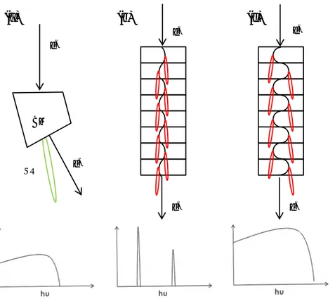
To be more specific, a storage ring is not perfectly circular but rather polygon and the straight sections are connected to each other by vacuum pipes with an angle. The electrons are bent in the ring mainly by bending magnets, which are pairs of big magnets. In the straight sections of 3rd generation storage rings, insertion devices such as wigglers and undulators are also installed to enhance the brilliance. These insertion devices have rather similar structures, both comprising of a periodic magnet array. However the magnetic field applied in a wiggler is stronger than the one for the undulator, which results in higher energies and a continuous spectrum as well as larger divergence than from an undulator (See Figure 2-1). To maximize the intensity of the photon energy coming out of the undulator, the undulator gap should be adjusted properly.
The generated light in the storage ring will be conducted to the beamlines with experimental equipment besides the monochromator and focusing components. The experiments in this work are mostly done at beamline I-511 (hv: 100 eV-1500 eV) which is an undulator-based beamline for UHV surface science research. Some of the experiments are completed at the beamline D-1011 (hv: 30 eV-1600 eV) which is a bending magnet beamline.
Figure 2-1: Schematics of the electron trajectories and the photon spectrum generated by in (a) bending magnet, (b)
undulator and (c) wiggler.
2.2: Spectroscopy Techniques
2.2.1. X-ray Photoemission Spectroscopy
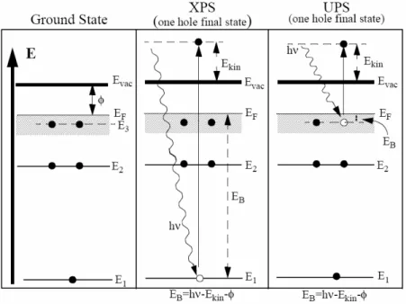
Photoelectron spectroscopy (PES) is a powerful experimental technique that provides information about the occupied electronic states of molecules or solids. This technique is based on the photoelectric effect which was discovered by Heinrich Hertz in 1887 and later explained theoretically by Albert Einstein that the photon energy depends on the frequency of the light rather than the intensity.
Electrons in materials can be excited to higher energy levels upon exposure to the light. When photons hit the material, electrons absorb the photons and if the incident photon has high enough energy, these electrons (photoelectrons) overcome the material’s energy barrier (work function) and enter the vacuum (continuum state). A schematic view of the photoemission process is shown in Figure 2-2.
e -BM e -SR e -e -e -e -(a) (b) (c)
Figure 2-2: The photoemission process (XPS and UPS). In core level photoemission by illumination of photon of proper
energy, a core electron is excited above the vacuum level. In UPS, the radiated photon lifts an electron from the valence band to the continuum.
When applying photons with a well-defined energy hv, intensity of the emitted photoelectrons is
measured as a function of kinetic energy (𝐾𝐸) using an electron energy analyzer (electron
spectrometer). The binding energy (𝐸𝐵) of the photoelectron is then determined by the energy conservation law (equation 2.1), where Φ represents work function of the sample (energy difference between Fermi level and vacuum level)47.
𝐾𝐸 = ℎ𝑣 − 𝐸𝐵− 𝛷 (2.1)
The technique was developed by Prof. Kai Siegbahn in the 1950’s and was called Electron spectroscopy for chemical analysis (ESCA) and later denoted X-ray Photoelectron Spectroscopy (XPS)48. This technique is used to study the electronic structure, chemical composition and chemical bonds of molecules and solids.
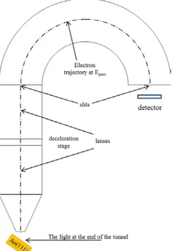
The photoelectron which found its way out of the sample’s surface is then collected by the photoelectron spectrometer. A schematic of the hemispherical analyzer is shown in Figure 2.3. There are retarding lenses at the entrance, which are used to adjust the incoming photoelectrons to the defined pass energy. The photoelectron then enters the hemispherical electrodes. The concentric hemispherical analyzer (CHA) possesses double layer structure electrodes, where inner and outer shells have different electrical potentials. These electrodes only conduct electrons with the desired kinetic energy to a micro-channel-plate (MCP) at the end of trajectory. The signal is enhanced using cascade amplifiers. A large number of electrons hit the phosphorescence screen and the signal will be recorded on a charge-coupled-device (CCD) camera. Electrons with higher or lower kinetic energy than the pass energy collide with the electrodes.
Figure 0-3: The schematic view of the hemispherical electron energy analyzer.
Photoelectron spectroscopy is classified as X-ray photoelectron spectroscopy (XPS) and Ultraviolet photoelectron spectroscopy (UPS), depending on the incident photon energy. However, since nowadays synchrotron sources allow us to choose the photon energy in a wide and continuous range of energies from UV to soft x-ray, the border between these two photoemission spectroscopies is not explicit.
Cross section
As mentioned above, even though synchrotron facilities give us the opportunity to select any photon energy from the spectrum of a fairly large window, one should keep in mind photon-electron interaction cross-section in order to choose the proper photon energy. Electrons from the same orbital can be excited with different quantum efficiencies depending on the photon energy, which makes it important to consider this fact while selecting the photon energy for measurements. A complete set of the cross section for 103 atoms at different photon energies are published by Yeh and Lindau49, guiding us to choose the proper photon energy to probe the molecular orbitals.
Mean free path
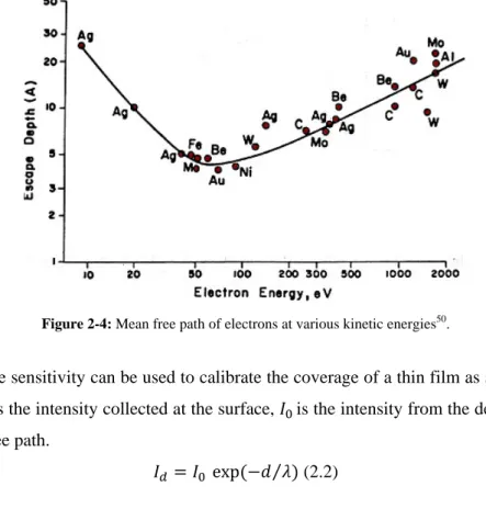
Another point which one has to consider, when selecting a photon energy for photoemission experiments is the scattering of the electron inside the matter. The excited electron can be inelastically scattered by phonons or plasmon excitations. X-rays can penetrate deep in to solids (µm range), but actually the detected photoelectron in the photoemission experiments come from the topmost atomic layers, since the interaction with the matter is much stronger. From the electrons which reach the
analyzer, only the elastically scattered ones will contribute to the main peak of the photoemission spectrum. The distance an electron can travel inside the matter without experiencing inelastic scattering is called “mean free path”. This distance is defined more by the kinetic energy of the electron rather than the type of matter. In fact since the average length that an electron travels will be reduced by elastic scattering processes, and consequently probability of inelastic losses become higher, the kinetic energy of the excited electron plays an important role, determining this travel distance. The mean free path versus kinetic energy curve is given in Figure 2.4 and shows the surface sensitive energy range. This curve which is called the “universal curve” exhibits that electrons with kinetic energy between 50 to 100 eV show the minimum mean free path, and electrons with kinetic energy higher or lower than this kinetic energy, have larger probe depth. This decreases the surface sensitivity. By increasing the thickness of the upper layer, intensity of the substrate declines exponentially.
Figure 2-4: Mean free path of electrons at various kinetic energies50.
Therefore, surface sensitivity can be used to calibrate the coverage of a thin film as shown in equation (2.2), where 𝐼𝑑 is the intensity collected at the surface, 𝐼0 is the intensity from the depth d and 𝜆 is the inelastic mean free path.
𝐼𝑑 = 𝐼0 exp(−𝑑 𝜆⁄ ) (2.2)
Emission angle
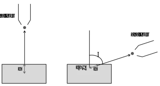
Besides the kinetic energy, the emission angle also affects the surface sensitivity. Two different commonly used emission angles (normal and grazing emission) are depicted in Figure 2.6. Going from normal emission to grazing emission, the photoelectron has to travel longer to reach the vacuum and escape the surface, which would cause higher probability of inelastic scattering for the excited electron from some depth, letting only the surface-area electrons make it out of the surface and reach the analyzer.
Figure 2.5: illustration of increasing the surface sensitivity in photoemission experiments, by going from normal emission to
grazing emission. Mean free path (d) is the same in both cases; however in grazing emission the probe depth is smaller than in normal emission, which results in higher surface sensitivity achieved in grazing emission.
XP spectrum
In an x-ray photoelectron spectrum, the number of collected electrons as a function of binding energy is displayed (Figure 2.6.). The electron binding energies are element-specific and specific for each particular level inside an atom. Even though core electrons are localized and do not participate in chemical bonds, they will be influenced by any variation in the charge distribution of valence bands. These variations can be due to initial or final state effects and can give a shift (called chemical shift) to the core-level spectra. Initial state effects are the shifts which are related to the ground state system and are caused by electron-density-induced binding-energy changes. On the other hand final state effects appear in the core-excited state of the system; when an electron leaves the matter, screening of the core hole and refilling induce changes in the spectrum which are considered as final state effects. The origin of chemical shifts is the surrounding electronic environment and neighboring atoms. In other words, an electron rich environment shifts the core level to lower BE, whereas a low electron density environment shifts the core level to higher BE.
But before making further interpretation of XPS results, an energy calibration should be done. For solid systems, the zero energy is chosen at the Femi level. For metallic substrates, Fermi level is measured directly on the sample, though for the semiconductor sample it had to be measured on a metallic (Tantalum) foil in direct electrical contact with the substrate.
d dcos 𝜃
𝜃 analyzer
analyzer
Normal emission Grazing emission
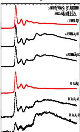
Figure 2.6: N1s spectra of ZnPc on Pt(111). From bottom to top: sub monolayer of ZnPc, monolayer and the thick film. The
shift between N1 of the sub-ML and N2 of the TF is a final state effect. N1 and N2 are the two chemically shifted spectra, corresponding to the molecules at the first and second layer on Pt respectively. SUN1 and SUN2 are the shake-up structures.
Resolution
Another concept to be considered for an XP spectrum is the resolution. The parameters affecting the resolution give two types of peak broadening; the first group gives a Gaussian broadening to the peak. Mostly external parameters such as light source, optical components and detector contribute to the Gaussian width, but phonon excitations and different chemical components can also affect the Gaussian width. The second group contributes to the Lorentzian width, which corresponds to the core-hole lifetime. In some cases curve-fitting applying Voigt (Gaussian-Lorentzian) functions should be done, in order to distinguish the different contributions. For example, in case where the shift between different chemical components is not easily resolved in the spectrum, by curve-fitting one can deconvolute the different peaks, which can give invaluable information about the studied system. An example is presented in Figure 2.6, showing two different N1s peaks of Zinc Phthalocyanine adsorbed on Pt(111), which are chemically shifted with respect to each other due to different interaction with the substrate.
In a spectrum such as the ML in Figure 2.6, different relative intensities for different peaks are observed, which simply correlate with the number of each atom. However diffraction effects22 and photoionization cross-section issues can vary the ratio between the different peaks.
403 402 401 400 399 398 397 396 395 Int ens it y( ar b. uni t) TF ML sub-ML N1s, hv:490 eV ZnPc-Pt(111) SUN1 SUN2 N2 N 2 N1 Binding Energy(eV)
Satellites
Additional features at higher binding energy of the main peak of the photoelectron spectrum are often observed. These features which are called satellites, appear when an excitation in the molecular valence levels takes place at the same time as the photoelectron is ejected. If the valence electrons are excited to bound states, the satellite is called shake-up. This secondary excitation in semiconductors appears as an extra peak and since this excitation reduces the photoelectron kinetic energy, the additional peak appears at the higher binding energy than the main peak. In semiconductors, the minimum energy an electron in the valence band needs to be excited to the conduction band is equal to the band gap. The difference in the binding energy of this shift peak corresponds to the band gap of the semiconductor. In the organic semiconductors, the observed shake-up structure is the consequence of excitation of an electron from HOMO (Highest Occupied Molecular Orbital) to LUMO (Lowest Unoccupied Molecular Orbital) of the molecule, and the shift from the main peak is equal to the HOMO-LUMO gap51. If the photoelectron is emitted to vacuum, similar to shake-up there will be a satellite which is described as a shake-off. The shake-off structures appear in higher binding energies than shake-ups47.
In metals, instead of an additional peak, a difference in the photoelectron spectrum’s line-shape is observed. Upon exciting an electron from the valence band of the metal surface to its conduction band, while the photoelectron is emitted, a reduction in the photoelectron kinetic energy takes place. This reduction in the photoelectron’s kinetic energy gives rise to intensity on the low-kinetic energy side which is translated to be the high-binding energy side. Therefore, when fitting the spectra from metallic surfaces, an asymmetry factor has to be considered, which gives a “Doniach-Sunjic” line shape.
2.2.2. X-ray Absorption Spectroscopy
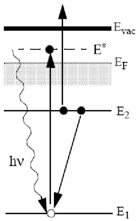
X-ray absorption spectroscopy (XAS) also known as “near edge x-ray absorption fine structure” (NEXAFS) is another surface sensitive method which is applied to study the electronic structure of the empty states (unoccupied orbitals in molecules and conduction band in solids). The absorption process is shown in Figure 2.7 schematically. This technique deals with structure up to 30 eV above the absorption edge.
Figure 2.7: Schematic representation of the x-ray absorption process.
In this method, an X-ray photon is absorbed as its energy is scanned through the absorption edge. Since the photon energy needs to be scanned continuously, these types of measurements require a tunable source in a relatively large energy window, and synchrotron radiation is the solution for it. Once the incident photon is of sufficient energy, it can lift the core electron to an unoccupied state, which leaves the sample in an unstable situation. But this core hole will be filled by another electron, either radiatively by fluorescence decay or non-radiatively via Auger decay. The screening of the created core hole is done within femto- to attoseconds time frame. The final state of the XAS is the main difference between this method and XPS, since XAS possess a “self-screened” final state. In XPS, since the photoelectron leaves the sample and enters the vacuum, screening has to be done by the surrounding electronic environment. The significant experimental characterization of XAS is the ability to map the unoccupied states, whereas XPS provides the information of the occupied states. Besides, both methods are element specific and also chemically specific (responds differently to different electronic environment of the same atom); hence these two methods, as complementary methods to each other can deliver broad and detailed information about different electronic states of the studied system.
Different methods can be used to detect and record an XA spectrum, depending on the equipment and the field of research. These possible methods are: transmission, fluorescence and Auger decay. Transmission is when the intensity of transmitted X-ray is measured before and after the sample. This seems to be a straightforward technique; however it requires a very thin solid film. It can also be used in the measurement on liquids due to their higher penetration depth with respect to solid matters. Fluorescence decay can be measured by a fluorescence detector but the dominant decay, following K
edge excitations for low-Z elements (Z: atomic number) is Auger decay, since typically in an absorption process, both Auger processes and photoemission processes take place (Auger peaks are recognized by their fixed kinetic energy). Therefore since in this work K edge of N and C are measured, we have used Auger decay methods.
Auger decay methods are classified in three categories. First one is Total Electron Yield (TEY) which has contribution from both elastically- and inelastically-scattered electrons. Since inelastically scattered electrons bring information from a deeper region, this method is mostly used for bulk studies. By applying a retarding voltage in Partial yield method and filtering the low kinetic energy electrons, surface sensitivity is enhanced. The third method based on Auger decay is the Auger electron yield (AEY) which is somehow different from the first two. In this case, we use the photoelectron spectrometer to detect the electrons, since this would make it possible to measure constant-kinetic-energy Auger electrons. This kinetic energy is the kinetic energy of the desired Auger peak, and the photon energy range normally starts just below the absorption edge. Number of Auger electrons (intensity) depends on the number of excited electrons, and that itself depend on the absorption cross-section. This method (AEY) provides the most surface sensitive detection technique. In this thesis, the XAS data are collected with both TEY (at the beamline D-1011, MAX lab) and AEY (at the former beamline I-511, MAX lab).
Intensity of the recorded spectrum might have contributions from the light intensity correlated with the incident photon energy and continuous movement of monochromator and insertion devices while scanning the photon energy. It also might be influenced by the contamination of the optical components along the beamline. Therefore it is necessary to calibrate the intensity by recording the photocurrent at the gold mesh just in front of the sample and dividing the XAS data to this recorded current. To remove the contributions of contaminations, the spectrum can be normalized to the spectrum recorded from the clean substrate. In this way the useful data will be separated from contributions of the background. Not only the photon intensities, but also their energy should be calibrated. This is done by measuring the kinetic energy of a core level with the first and second order light, keeping the monochromator fixed. The difference in the measured energy gives the actual photon energy.
The first resonance in the spectrum, as shown in the Figure 2-8 represents the transition from the core level to the lowest unoccupied molecular orbital (LUMO) typically a 𝜋∗ and the broad peak at higher photon energy corresponds to the transition from the core level to 𝜎∗ states. The system is perturbed upon XAS. This affects the resonance peaks in the XA spectrum. 𝜋∗ states which are located just below or above the vacuum level, can be shifted all the way down below the Fermi level and for the first resonance peak, it might even be lower than the binding energy of the same core level binding energy measured by photoemission. This shift to lower energy is described by the Coulomb potential between core-hole and the excited electron. However delocalized weakly-bound 𝜎∗ states are located
above the vacuum level. This causes a shorter lifetime for the excited electron in comparison with the one excited to 𝜋∗ and this short lifetime leads to broadening of the peak.
Figure 2-8: N K-edge XAS of a monolayer and a thick film of ZnPc on Pt(111), showing that ZnPc molecules are almost flat
in the ML regime, but tilted at the TF.
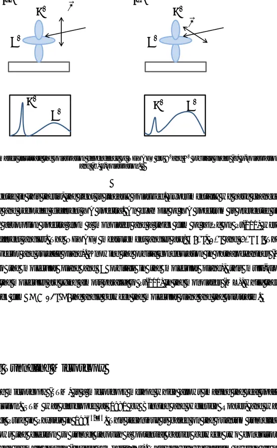
One of the significant points about XAS is that it enables us to determine the orientation of the adsorbed molecules with respect to the substrate. Intensity of resonances in XA spectra is directly proportional to the absorption cross-section, which is highly angular dependent. As a consequence of this, the angle between the light polarization and the molecular orbital influences the intensity of that resonance peak. In Figure 2-9, the schematic of the relation between the light polarization angle and molecular orientation is illustrated. This means that by tracing the intensity variation as a function of changing the angle, one should be able to determine the orientation of the adsorbed molecules on the substrate. 395 400 405 410 415 420 Thick-G NEXAFS N K-edge ZnPc/Pt(111) Thick-NE Int ens it y ( ar b. uni t) Thick-NI ML-G ML-NE
Binding Energy (eV)
Figure 2-9: The schematics illustrate the polarization dependence of NEXAFS for 𝝅∗and 𝝈∗ orbitals under (a) p-polarization and (b) s-polarization.
In the work presented in this thesis, the light is linearly polarized. Experimentally we have changed the incident angle and recorded different XA spectra. An example of XA spectrum is presented in Figure 2-8. X-ray absorption spectra from a monolayer and a thick film of ZnPc on Pt(111) were measured in 3 different angles. The NEXAFS measurement angles are: 𝜃: 0°, 40° and 80°(𝜃: The angle between E vector and surface plane). Knowing the orbital configuration in phthalocyanines (𝜋 orbitals normal to the molecular plane and 𝜎 orbitals in the molecular plane), this multi-plot demonstrates that the molecules are lying almost parallel to Pt(111) in the monolayer (ML), while they are tilted in the thick film (𝜑 < 45°, 𝜑: the angle between the molecular plane and the substrate).
2.3: Scanning Tunneling Microscopy
Scanning tunneling microscopy (STM) is a microscopy method which allows imaging the real space with atomic resolution. STM was developed at 1981 by Binning and Heinrich Rohrer, and was awarded the Nobel Prize in Physics in 198652–54. This technique is based on the quantum tunneling effect, which allows the electron to tunnel through a potential barrier between two conductors provided that the gap is small enough (couple of Ångströms). This gap can be vacuum or even air or liquid, where the energy of the potential barrier is larger than the energy of tunneling electron. Tunneling effect is the result of overlap between the wave function of two conductive surfaces, i.e. the transition takes place via this wave function overlap despite the gap of a few Ångströms. In this case,
𝜋
∗𝜎
∗𝐸
𝜋
∗𝜎
∗𝐸
(a)
(b)
𝜎
∗𝜋
∗𝜎
∗𝜋
∗electrons can tunnel in both directions, from one conductor to another, causing a zero net current. In order to achieve a net current, a bias is applied between the two conductors.
In an experimental STM set up, a very sharp (ideally monoatomically sharp) conductive tip (commonly made of W or Pt-Ir) scans over a relatively flat surface. The surface has to be metal or semiconductor for the tunneling effect to happen. Since the distance between the tip and the sample should be kept very small (couple of Å), roughness of the sample should not be too high, which would result in either disturbing the tunneling during the measurement or crashing the scanning tip. Therefore, this measurement requires samples of high quality and careful surface –science sample preparations.
As mentioned earlier, in order to control the direction of electron tunneling, a voltage should be applied between the conductive surfaces. So we need to add a small bias between the tip and the conductive sample. Depending on the polarity of the applied voltage, electrons can tunnel to or from the tip. Schematic illustration of energy levels corresponding to the sample and the tip is presented in Figure 2-10.
Figure 2-10: A schematic representation of the principle of STM, for (a) zero bias voltage, (b) positive bias voltage and (c) negative bias
voltage. (Figure taken from55)
As shown in Figure 2-10, if a negative bias is applied to the sample, the electron flow is from the sample to the tip. These electrons are from the occupied states of the sample which will tunnel to the tip, giving information about occupied states of the sample. On the other hand, applying a positive bias to the sample changes the electron flow; from the tip to the sample. These electrons will tunnel to the unoccupied states of the sample (unoccupied molecular states or conduction band states), carrying information of the unoccupied electronic states of the sample.
(a)
(b)
As explained above, the basic principle of STM is the quantum tunneling effect, in which the tunneling current has an exponential relation with the distance between the two conductors. (See equation 2.3). This correspondence enables this technique to map the topography as well as the electronic structure of the studied sample’s surface by simply scanning over it.
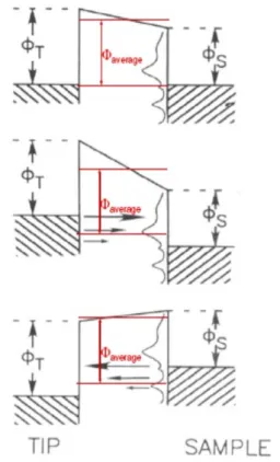
𝐼 ∝ exp �−2𝑑�2𝑚�𝛷𝑎𝑣𝑒𝑟𝑎𝑔𝑒ħ −𝐸�� (2.3)
In Figure 2-11, schematic view of STM setup is demonstrated. The function of STM can simply be described as following. A coarse motion moves the tip towards the surface until the distance is small enough for tunneling to take place. This is controlled by the applied voltage and the reference tunneling current. From this position, the tip’s motion is controlled by piezo components, usually X, Y and Z components. X and Y are used to scan the tip over the sample and the Z component is responsible for adjusting the tip-surface distance. The tip’s Z control is done in different ways, determined by the imaging mode.
Figure 2-11: Schematic of STM (Courtesy to Michael Schmid, TU Wien)
Imaging with STM can be carried out, using two different methods. These imaging modes are known as constant-current and constant-height modes. In constant-current mode, the tunneling current signal which is transferred to the control unit will be compared to the set-point in the feedback loop. Then, the control unit sends a signal to the Z component to change the height until the tunneling current matches the set-point. Variations in the tip position provide a topographical map of the surface, which will be recorded as an STM image. The other imaging mode is the constant-height mode, in which the tip-surface distance is kept fixed and the feedback loop is not active. Variations of tip position, which keep its distance constant from the surface, correspond to the topography of the surface and cause
fluctuations in the tunneling current. These current changes will be translated to topography in the calibrated control unit. The drawback of the constant-height mode is that the feedback loop, which can control the tip-surface distance and prevent the tip from crashing is deactivated. Hence the constant current mode is the most common imaging mode in tunneling microscopy.
The extremely small tip-surface distance together with the highly precise piezo movement, results in very high resolution obtained in this microscopy technique (0.01 Å, vertical resolution and about 2 Å, lateral resolution), which makes it a highly local tool to probe the electronic properties of surfaces. Giving an atomically resolved image of surfaces and adsorbate layers, STM provides the opportunity to investigate the atomic arrangements at the surface and possible surface reconstructions.
The STM images presented in this thesis are obtained via two different microscopes; Omicron VT-STM and RHK (UHV SPM 3500). In both cases, measurements are performed in UHV and in-situ sample preparations are carried out. Image processing is done using WxSM. (more details on preparation methods are mentioned in the articles.)
2.4: Low Energy Electron Diffraction
Low energy electron diffraction is a technique employing elastic scattering of electrons from the surface to reveal information about the surface reconstructions. Importance of the investigation on atomic orders at the surface comes from the fact that sometimes atoms arrange themselves differently at the surface of a material with respect to the bulk, causing changes in the unit cell parameter. These new arrangements as result of relaxation or reconstruction take place to reduce the total energy. Elastic scattering or diffraction of electrons is a standard technique to obtain structural information of surfaces56. The basic diffraction condition in LEED can be described the same as in x-ray diffraction. The scattering parameter should satisfy Bragg’s law (equation 2.4).
𝑛𝜆 = 2𝑑 sin 𝜃 (2.4)
(“n”: an integer, λ: the wavelength of incident wave, d: the spacing between the planes in the atomic lattice and θ: the angle between the incident ray and the scattering planes.)
Results of a LEED measurement contain information of the unit cell parameter as well as the location of atoms in this unit cell. Information of the former (lattice parameter) is extracted by a reverse transformation, since the diffraction pattern corresponds to reciprocal lattice. However determination of the coordination of atoms requires detailed studies, which is not included in the scope of this work. The experimental setup for LEED comprises of the following parts; an electron gun to produce the electron beam and a display system to show the Bragg diffraction spots. A typical four-grid LEED system is shown in Figure 2-12.
Figure 2-12: The schematic of a four-grid LEED optics.
The electron gun is located in the center of the diffractometer. The electron gun produces an electron beam with the beam diameter of about 1mm or less and the energy range ~ 10-500 eV. The LEED experiment is based on the electron acceleration from the electron gun. Acceleration occurs by applying a variable voltage which affects the kinetic energy of the emitted electrons. Once the electrons hit the sample, they will be diffracted and pass through vacuum toward a series of grids. To get a field-free region, the first grid is grounded; in second and third ones variable voltage (the suppress voltage) is applied to filter out the inelastically scattered electrons. A high voltage is applied between fourth grid and the screen which gives the electrons enough energy to light up the phosphor screen and reveal the diffraction pattern.
The electron wavelength is given by de Broglie equation 2.5. 𝜆 =√2𝑚𝐸ℎ (2.5)
In this equation, h is Planck’s constant, m is the electron mass and E, the energy of electrons.
Since the interatomic distances in solids are a few Å, the electron wavelengths are selected in this range, meaning the acceleration energy of the electrons in the electron beam is about 30 to 500 volts. Recording and analysis of the diffraction pattern reveals the arrangement of the atoms on the surface. Also sharpness of the pattern describes the extent of order of atoms on the surface.
In Figure 2-13(a), an example of a LEED pattern is demonstrated, in which the Au(111)-I (5 × √3) reconstruction is depicted. Figure 2-13(b), shows a calculated pattern of the same reconstruction.
Figure 2-13: (a) and (b) are the measured and calculated LEED pattern
of the Au(111)-I(5 × √3) surface reconstruction. 5𝑥√3
Chapter 3
Adsorbates and Substrates
3.1: Adsorbates
3.1.1. Metal-Phthalocyanines (MPcs)
Phthalocyanines are synthetic macro cyclic compounds, constructed of four lobes; each lobe is
composed of one pyrrole and one benzene group. Metal-free phthalocyanine (H2Pc) is noted as
H2C32N8H16 (Figure 3-1(a)). The flexibility of this molecule provides an opportunity to replace the two central H atoms with a metallic atom (MPc) (a metal-oxygen or metal-halogen can also be inserted to Pc center). Depending on what would occupy the center, the molecule can possess a planar or a non-planar configuration. In most cases the molecule remains non-planar except when a big metallic atom e.g, Sn or Pb occupies the center. Moreover, if a polar component such as TiO replaces the two H atoms in the center, the molecule will possess a shuttle-shaped geometry.
The various features, such as electronic, optical and magnetic properties of Pcs can be tuned by changing the metallic center57–61. In particular, transition metal phthalocyanines has gained lots of attention, owing to the significant effect of d-orbitals on properties of the molecules21–23,62–72.
These molecules can create self-assembled layers, making the thin film processing very convenient23,57,58,62,73–76. These intrinsically semiconducting molecules, show a very high thermal (stable up to 500℃) and chemical stability in addition to their electronic, optical and magnetic properties. These characteristics make MPc a promising candidate to be used in organic solar cells, organic light-emitting diodes (OLEDs) and organic field-effect transistors (OFETs). The function of these devices is influenced by another essential factor; the interaction and charge transfer at the interface of MPc layers and the substrate. Charge transfer at the interface of MPc and the substrate can determine the layer growth mode, molecular configuration, magnetic and electric properties of the molecular layer, which would effectively modify the organic-device functions. More manipulation of MPc-substrate interaction is possible by either decorating the molecules (adding external atoms or molecules to the center or periphery of Pcs)35–37 or modifying the substrate by inserting an intermediate layer38,39. Adding a layer on top of MPc-substrate has been also reported40–44.
In this thesis MgPc, FePc and ZnPc are studied. In MgPc and ZnPc, HOMO (Highest Occupied Molecular Orbital) and LUMO (Lowest Unoccupied Molecular Orbital) have only contributions from organic ligand, while HOMO and LUMO of FePc have considerable contributions from Fe d orbitals. This is described by d orbital of Fe being open-shell type while Zn has a closed d-shell. Zn2+ and Mg2+ show a similar electronic configuration having fully filled sub-shells. However adsorption of these molecules on different substrates results in change in the orbital configuration and the participation of each orbital in interfacial interactions.
3.1.2. 4-tert-butyl pyridine (4TBP)
4tert-butylpyridine is a heterocyclic molecule which possesses the structure of a pyridine, in which one of the hydrogen atoms (position 4) is replaced by a tert-butyl [−𝐶(𝐶𝐻3)3] group. The schematic illustration of chemical formula of both pyridine and 4tert-butyl pyridine (4TBP) is presented in Figure 3-2. Pyridine itself is actually made of a benzene ring which has accommodated a nitrogen atom by replacing a methine-group (𝐶 − 𝐻) with the chemical formula of C5H5N. Pyridine is a colorless liquid which is soluble in water. It is a weakly alkaline, highly flammable compound with unpleasant fish-like smell. 4TBP is known to be a significant additive to the electrolyte of DSSCs. There have been several works which have investigated the effect of 4TBP on the function of DSSCs. Following results have been reported.
Figure 3-2: Chemical formula of (a) pyridine and (b) 4.tert-butyl pyridine (4TBP).
Upon addition of 4TBP to the (I3
-/I-) electrolyte, the fill factor and open circuit voltage are increased without affecting the short circuit current46. These effects are described by occupying active sites of TiO2 by 4TBP
77 .
In different studies, a 4TBP-induced shift of the conduction band edge of TiO2 to lower binding
energies was found to be responsible for enhancement of open circuit voltage. Moreover, 4TBP
reduces the concentration of protons and other cations in the electrolyte and remove them from the substrate. These cations are known to induce band bending in TiO2 conduction band edge in the opposite way as 4TBP. Besides, 4TBP blocks the transport of tri-iodide to the surface and removes adsorbed iodine from the surface reducing the electron recombination from TiO2 to tri-iodide in the electrolyte78,79.
3.2: Substrates
3.2.1. Au(111) and iodated surfaces
Au(111)
The clean Au(111) surface has a (22× √3) reconstruction80, also known as the herringbone structure. This surface is the only (111) surface between closed-pack fcc metals, which is reconstructed. In Figure 3-3, two STM images from the clean surface are presented. Figure 3-3(a) shows large flat terraces separated by monoatomic steps (1.3Å) and Figure 3-3(b) illustrates the herringbone structure. The herringbone structure consists of dark (lower) and bright (higher) regions. The surface plane of Au(111) has more atoms than the bulk plane (4% higher). The surface is described by a stacking-fault-domain model. In this surface, different areas (fcc and hcp) are periodically stacked. These two regions are separated by a domain wall (also known as soliton wall) from each other.
N
2
1
3
4
5
6
N
(a)
(b)
As Figure 3.3(b) shows, fcc and hcp areas appear darker in the STM image than the domain walls. It means that these regions (hcp and fcc) are located lower than domain walls, which appear as brighter stripes between the two hollow site regions. A closer look in the image reveals that the widths of the dark regions are different; wider regions have fcc and narrower ones have hcp stacking26.
Figure 3-3: STM images of Au (111) surface; (a) 300x300 nm2 showing large flat terraces separated by monoatomic steps (1.3 Å) and (b) 70x70 nm2 herringbone structure is visible. Fcc and hcp regions and soliton wall are marked panel (b).
Au(111)-I(√𝟑 × √𝟑)R30°
After iodine deposition, the herringbone structure disappears. One of the possible Au(111)-I structures is the (√3 × √3)R30°, which is a common organization found after deposition of smaller adsorbates on the (111) surface of transition metals81–83. This structure most often holds 1/3 monolayer (ML) of adatoms (1 ML corresponds to the number of gold atoms on the bulk terminated 111-surface). STM image and LEED pattern of this surface, together with the atomic model are presented in Figure 3-4.
Figure 3-4: (a), (b) and (c) are STM image (+0.38 V, 0.7 nA), LEED pattern and atomic model of the Au(111)-I�√𝟑 ×
√𝟑�𝑹𝟑𝟎° surface. The unit cell is outlined in the model.
In the present case, it was suggested based on IV-LEED that every iodine atom is in contact with three gold atoms in the hcp-hollow sites84. Our calculations give a slight preference for the fcc site as some other theoretical studies of the halogen adsorption on transition metal surfaces did, however the energy difference between the two sites is very small85,86. STM and LEED (as used here) are not able
Fcc region Hcp region Soliton wall
to tell the difference between these two sites, therefore an atomic model of this reconstruction in Figure 3-4(c) is presented with iodine atoms in (unspecified) hollow sites.
Au(111)-I (𝟓 × √𝟑)
At the saturation limit for our deposition method, a (5 × √3) structure was achieved. Higher coverage structures are only observed with an over-pressure of iodine83 or in electrochemical conditions. The STM image in Figure 3-5(a) displays the surface with atomic resolution, which fits nicely with the atomic positions in the structure model on the right hand side (Figure 3-5). This structure has been observed by STM81,87 and LEED88 as discussed previously, and is known to appear in the coverage range 0.33<𝜃<0.4. Surface X-ray Scattering (SXS) measurements in electrochemical conditions have also reported (p× √3) structures with p varying with the applied electrochemical potential, suggesting an uni-axial compression of the (√3 × √3)R30° structure to form a striped phase82.
Figure 3-5: (a), (b) and c are STM image (-0.27 V, 8.1 nA), LEED pattern and atomic model of the Au(111)I-(5×√3)
structure. The unit cell is outlined in the model.
Basically by compressing the (√3 × √3) structure perpendicular to one of the √3 directions, a higher coverage of iodine can be accommodated on the substrate, which eventually will lead to a (5 × √3) LEED pattern88. The compression inevitably forces some iodine away from their hollow (hcp) sites into bridge and the other hollow (fcc)88. Thus, whether iodine sits in the fcc or hcp hollow on the (√3 × √3) structure does not affect the positions in the (5 × √3) reconstruction.
3.2.2. Pt(111) and iodated surface
Pt(111)
As mentioned in section 3.2.1, fcc(111) closed-packed surfaces excluding Au, do not reconstruct. For an ideally terminated Pt(111), the top interlayer spacing is prominently expanded by 0.025 ± 0.01 Å (1.1%). Charge reorganization at the surface induces strengthening of intralayer bonding in expense of interlayer bonding, causing the expansion of the first metal layer spacing89.
Pt(111)I-(√𝟑 × √𝟑)𝑹𝟑𝟎°
At 1/3 ML iodine coverage on Pt(111) is reconstructed to a (√3 × √3)𝑅30°. At this layer iodine atoms only sit on 3-fold sites which provide stronger Pt-I bonding. The (√3 × √3) model is given in Figure 3-4, the same as for Au(111)-I (√3 × √3).
Pt(111)I-(√𝟕 × √𝟕)𝑹𝟏𝟗°
Further adsorption of iodine on Pt, creates a saturated layer with a �√7 × √7�𝑅19° reconstruction (see Figure 3.6).
Figure 3-6: atomic model of the Pt(111)-I �√𝟕 × √𝟕�𝑹𝟏𝟗° structure.
This reconstruction is confirmed by our LEED investigations. In this layer iodine atoms occupy three different sites, 3-fold sites (hcp and fcc) and atop sites90. (The 3-fold sites are not equivalent, there are two different 3-fold sites; one with a Pt atom directly under and the other one without. The ones with a Pt atom directly under are more favored for electronegative adatom (iodine in this case)). Photoelectron spectroscopy results from I4d enable us to distinguish the iodine atoms in 3-fold and 1-fold (atop) sites (discussed in paper III).
3.2.3. TiO
2(110)
Rutile TiO
2There are three diverse crystallographic modifications of titanium dioxide called rutile, anatase, and brookite. Rutile is the most common one in research due its various technological applications such as, photo assisted heterogeneous catalysis, energy conversion, gas sensors and protection layers. In this thesis only single crystalline rutile has been used.
In the rutile bulk structure Ti4+ ions are six fold coordinated while O2- is three fold coordinated. There are two formula units in each unit cell. Having a relatively wide band gap, 3.1 eV, rutile TiO2 is often considered an insulator in which the valence band is mostly made of O2p orbitals and the conduction band is mostly Ti3d derived91,92.
Pure TiO2 crystals are transparent. However, intrinsic defects (like oxygen vacancies or Ti interstitials) affect the conductivity and optical properties of the crystal. For example, the transparent crystal becomes light or dark blue, depending on the amount of defects. The transformation is consequence of sample reduction, which can be carried out simply by heating the sample (up to ~1000 K for a few hours) in UHV. This is done on purpose in the initial steps of sample preparation to enhance the conductivity of the sample. Upon this heat treatment, sample changes to an n-type semiconductor which allows STM measurements. Besides, the charging problem during XPS and LEED measurements will be avoided by reduction of TiO2.
The (110) surface
The (110) surface is the most stable surface in the rutile crystal structure, with the lowest surface energy and because of that they are formed in microscopic crystals. The schematic of the rutile (110) surface is given in Figure 3-7.
Through formation of a surface, bonds are broken, which generates atoms with different co-ordination than in the bulk. Titanium ions are 6-fold coordinated in the bulk. At the surface there are two different types; 6 fold coordinated, Ti6f, and 5-fold coordinated, Ti5f. There are also different oxygen ions; Osub are 3-coordinated oxygen ions in the bulk. O3f, are 3-fold coordinated oxygen ions at the surface. In addition there is also 2-fold coordinated (bridging) oxygen, O2f, which binds to two Ti6f. So the surface has rows of Ti-ions and rows of bridging oxygen.
In STM images from this surface one can see dark and bright rows, which correspond to Ti and O rows. The brighter rows are Ti and the darker run along the oxygen rows. The rows are separated by ~ 6.5 Å. In addition there are numerous bright spots in the oxygen rows. They are due to oxygen vacancies, formed by removal of bridging oxygen. The amount of oxygen vacancies depends on the sample history, time and temperature of heating. By creation of the bridging oxygen vacancy, two associated electrons will be left behind and they result in formation of Ti3+ ions. The STM image was
achieved by applying a negative bias, i.e, tunneling from occupied states of TiO2. The oxygen
vacancies are electron rich and therefore appear brighter in the image. Oxygen vacancies at the surface act as dopants and play a crucial role for the reactivity.
Figure 3-8: Filled state STM image from the TiO2(110) surface with plenty of oxygen vacancies (bright spots).
The effect of surface oxygen vacancies is perhaps most visible in valence band spectra. In Figure 3-9 two photoemission spectra from TiO2(110) at low binding energy are shown
93
. The two vertical lines in the figure indicate the valence band edge and the Fermi level, respectively. The top spectrum is from the clean (1 × 1) surface with a strong state in the bulk band gap. The origin is the oxygen vacancies on the surface. By adsorption of 4TBP, lower spectrum, the intensity is reduced. Depending on the sample history etc, it is not always possible to remove this state. It has other contributions than surface oxygen vacancies.
Figure 3-9: Photoemission spectra from TiO2(110) before and after adsorption of 4TBP. The peak at 0.9 eV is due electrons in oxygen vacancies. Their intensity is reduced after 4TBP adsorption.
By elevating the time or temperature of heat treatment, the reduction is enhanced, which results in
dark blue sample, possessing a (1 × 2) reconstruction. An atomic model of the (1 × 2)
reconstruction is shown in figure 3-10. Large balls are oxygen and small balls are titanium. The rows of red O and black Ti together with the atoms just below form Ti2O3 like added rows on the surface. Further heat treatment leads to the so called (1 × 2) -cross linked (CL) surface. It is very similar to the (1 × 2) except that the added rows are broken and partly shifted.