DEPARTMENT OF TECHNOLOGY
A Study of LDMOS
Switched Mode Power Amplifiers
Ahmed Al Tanany
A Study of Switched Mode Power
Amplifiers using LDMOS
By
Ahmed Al Tanany
This work is done at Infineon Technologies, Sweden under supervision of :
Johan Sjöström
Hans Norström
Chen Qiang
The examiner from university of Gävle
Olof Bengtsson
A DISSERTATION
Submitted in partial fulfillment of the requirements
For the degree of
MASTER OF SCIENCE
(Electronics/Telecommunication Engineering)
UNIVERSITY OF GÄVLE
Abstract
This work focuses on different kinds of Switch Mode Power Amplifiers (SMPAs) using LDMOS technologies. It involves a literature study of different SMPA concepts. Choosing the suitable class that achieves the high efficiency was the base stone of this work. A push-pull class J power amplifier (PA) was designed with an integrated LC resonator inside the package using the bondwires and die capacitances. Analysis and motivation of the chosen class is included. Designing the suitable Input/Output printed circuit board (PCB) external circuits (i.e.; BALUN circuit, Matching network and DC bias network) was part of the work. This work is done by ADS simulation and showed a simulated result of about 70% drain efficiency for 34 W output power and 16 dB gain at 2.14 GHz. Study of the losses in each part of the design elements is also included. Another design at lower frequency (i.e.; at 0.94 GHz) was also simulated and compared to the previous design. The drain efficiency was 83% for 32 W output power and 15.4 dB Gain.
Acknowledgment
I would like to take the opportunity to acknowledge my indebtedness towards all the people who have helped me in all my tasks and works.
My sincere gratitude is directed to my supervisor; Johan Sjöström. He actively involved himself in the project and offered useful support at every stage of my project, reviewed my schematics, answered my all questions and provided me with books and reading material.
I am deeply grateful to my supervisors, Hans Norström and Chen Qiang for the support, help and patience they have shown, that have provided a good basis for the present thesis. I am grateful to Andreas Wiesbauer for his prompt interest and introducing me to the
Infineon branch in Sweden.
I would also like to thank Hans Brandberg, manager of the concept engineering, Infineon
Technologies, Sweden, for helping and encouraging during the time of preparing this
research.
My thanks are extended to all engineers at Infineon, especially; Tomas Åberg, Paul Andersson, Reza Bagger and Ted Johansson for the welcome and the talk that we had.
Again, thanks for all your valuable advice and friendly help!
My sincere thank to my examiner at University of Gävle, Olof Bengtsson for his help and detailed review during the preparation of this thesis.
I would like to acknowledge my friends and teachers at University of Gävle, Sweden who were kind enough to help me during my course work and teaching me with the best of their knowledge.
To the class of 2005 thank you for the very interesting and enjoyable two years! I would also like to thank my dear cousin Mohammed El-Tanani and my dear friend Ramadan Al Halabi for their encouragement and support that they gave to me throughout my study and my research.
I owe my loving thanks to my Parents, my Brothers, my sister and their families. They have supported me very much during my study and research abroad. Without their encouragement and understanding it would have been impossible for me to finish this work.
To my lovely country Palestine!
Table of Content
INTRODUCTION ... 1
1 SI-LDMOS CHARACTERISTICS AND MODELING ... 3
1.1 SI-LDMOSRF PROPERTIES... 3
1.2 INFINEON LDMOS TECHNOLOGY (GM8)... 4
1.3 LDMOSCAD MODELING... 4
1.3.1 Yang model... 5
1.3.1.1 Channel current modeling and elements extractions... 5
1.3.2 ELMO Model... 6
1.3.2.1 Intrinsic device model... 6
2 POWER AMPLIFIER: ESSENTIALS AND CLASSES... 7
2.1 POWER AMPLIFIER:FIGURE OF MERITS... 7
2.2 LOAD LINE THEORY... 8
2.3 POWER AMPLIFIER CLASSES... 9
2.3.1 Classical classes... 9
2.3.1.1 Class A power amplifier ... 9
2.3.1.2 Class B power amplifier...10
2.3.1.3 Class AB power amplifier...10
2.3.1.4 Class C power amplifier...11
2.3.1.5 Overdriven class AB power amplifier simulated example ...12
2.3.2 Switch mode power amplifiers... 15
2.3.2.1 Class D power amplifier ...15
2.3.2.2 Class E power amplifier...17
2.3.2.3 Class F power amplifier ...19
3 CLASS J POWER AMPLIFIER... 21
3.1 THEORY OF OPERATION... 21
3.2 CLASS J EXAMPLE... 21
3.3 CLASS J COMPARISON WITH CLASS E AND F-1... 29
3.3.1 Load line comparison... 29
3.3.2 Voltage and current waveforms... 30
3.3.3 Losses in the three classes ... 31
3.4 CLASS JPROS. AND CONS. ... 32
4 DESIGN STRATEGY... 33
4.1 SINGLE-ENDED AND PUSH-PULL... 33
4.1.1 Push-pull ... 33
4.1.2 Single-ended ... 33
4.1.3 Advantages of single-ended push-pull topology... 33
4.2 IDEA... 34
4.3 CIRCUIT DESIGN AND ANALYSIS... 35
4.4 INPUT MATCHING CIRCUIT... 36
4.5 BONDWIRE: THEORY AND DESIGN... 36
5 IN/OUT- PCB DESIGN ... 39
5.1 BALUNDESIGN... 39
5.1.1 BALUN Topologies ... 42
5.1.2 N-half wavelength balun ... 43
5.2 PCBIN/OUT MATCHING NETWORK... 46
5.3 DC-BIAS NETWORK... 46
6 SIMULATION, MEASUREMENTS AND DISCUSSIONS ... 47
6.1 SIMULATION AND RESULTS... 47
6.3.1 Package model ... 60
7 COMPARISON AND FUTURE WORK ... 63
7.1 COMPARISON WITH 0.94GHZ... 63
7.2 CONCLUSION... 65
7.3 FUTURE WORK... 66
REFERENCES ... 67
APPENDIX A. PACKAGE CHIP... 71
APPENDIX B. PCB SCHEMATICS... 73
APPENDIX C. MEASUREMENT AND NEW MODEL SIMULATION ... 79
C.1 BALUN MEASUREMENT AND MODEL... 79
C.2 OUTPUT MATCHING NETWORK... 80
C.3 OUTPUT PCB ... 81
C.4 INPUT MATCHING NETWORK... 82
Introduction
The demands of high capacity, faster services and connection security require developing new techniques for wireless communication. From analog transmission to digital, from second generation to third generation, from GSM to EDGE and WCDMA, etc…. These standards require new equipment to fulfill their operation. Power amplifiers (PAs) are a vital component in any RF transmitter. High efficiency, wider bandwidth, high linearity, high gain and high output power are needed in all the applications. However, it is hard to meet all these qualities in the power amplifier. Hence, a trade off between them should be made depending on the applications that intend to be used. The main trade off is usually done between the linearity and the efficiency, because the gain and the output power depend on the device (i.e., the transistor) transconductance and size, respectively [1]. Higher data rate in the 3rd generation mobile standard requires high output power, which in turn needs high efficiency to reduce the losses that appear as a heat and cause degradation of the device performance. Increasing the power efficiency is one of the primary research areas. Various PA classes are developed recently to meet the high efficiency requirement. The PA classes can not be used (without modification) in the applications that use the amplitude modulation. To achieve a high efficiency, the amplifier should be driven with large input signal which degrades the linearity required in the amplitude modulation systems. Various technologies of efficiency enhancement techniques are being under the spot of the research. Techniques like envelope tracking and load modulation is required to improve the linearity of the PA.
This work studies different classes with simulation. Choosing the suitable class to achieve the high efficiency was the base stone. Analysis and motivation of choosing the class is included. Moreover, it concern to build a suitable topology that fit the requirements of mobile base station and future development. Choosing the suitable IN/OUT-PCB (i.e.; BALUN circuit, Matching and DC bias networks) external circuits is part of the work. However, there is much work done previously with switched mode power amplifier. This work was based on discrete components. Recently, a CMCD amplifier was manufactured to attain 75.6% drain efficiency at 900 MHz frequency with output power 28.6 dBm (0.73 W) using discrete circuit elements [2]. A CMCD power amplifier for the base-station applications was also shown to achieve 60% drain efficiency with high output power (13 W) [3]. An amplifier from a closely related class-E/F with 85% drain efficiency at 7 MHz has also been reported [4]–[6]. The parasitic loss in the inductance degrades the efficiency. These losses can be reduced with using an integrated resonator inside the
package and the inductance resonator could be achieved by using the bondwires which has higher quality factor.
For my knowledge, this is the second published switch mode power amplifier (SMPA) work that integrates the resonator inside the package. The first one is done in [7], which use HBT technology and common resonator circuit for both push-pull dies having operating frequency of 0.7 GHz. For 2.14 GHz frequency, it is difficult to connect two dies with large number of bondwires, which is required by the resonator. Hence, a separate resonator for each die was used in this work with LDMOS technology.
The report starts with a theoretical study of the Si-LDMOS with ways of modelings the device in CAD programs. Chapter 2 discusses important issues for power amplifiers and theoretical analysis for most of the PA classes. Chapter 3 discusses the chosen class for the design, its results from the simulation, comparison with similar classes, and the motivation. Chapter 4 and 5 discuss the design strategy and the circuit topology used in this work. Chapter 6 shows the results from the simulation and the measurements. Finally, in chapter 7; a comparison was done between the 2.14 GHz design and a 0.94 GHz design, it also includes the conclusion and suggestions for future work.
1 Si-LDMOS
Characteristics and Modeling
Choosing the device and its technology is the essential key to get high performance for the qualities stated previously (i.e.; linearity, bandwidth, efficiency, gain, and output power). Among all the devices, Si-LDMOS is still the most widely used in the market. However, the research is still on going for other technologies (i.e.; GaN HEMT, GaAs HBT, etc…).
1.1 Si-LDMOS RF properties
Silicon Laterally double Diffused MOSFET transistor is widely used in high RF power
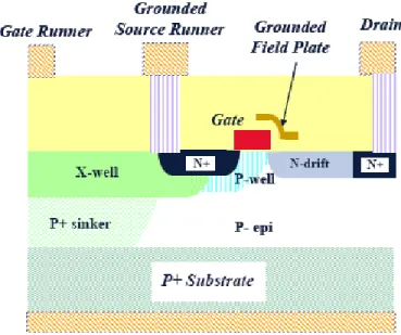
amplifiers below a few GHz. The main reasons are the maturated technology in terms of fabrication, the low cost and the reliability of silicon, combined with good performance. The cross sectional view of a Si-LDMOS is shown in Fig. 1.1. [8]. The LDMOS transistor is a modified device of the MOSFET to enhance the high power capability. The main modifications are:
1. Low doped and long n type drift region, which enhances the depletion region and increases the breakdown voltage. However the on-resistance is high which increases the losses and degrade the RF performance. Thus, there is always a trade-off between RF output power and on-resistance.
2. Short channel length created by laterally diffused P-type implantation, which increases the operating frequency. On the other hand, this feature increases the linearity since the electrons always transport in the saturation velocity.
3. The sinker principle is used to connect the source to the substrate backside, which reduces the source inductance, hence, the gain increases. Also the sinker makes the device integration much easier.
CH1: Si-LDMOS Characteristics and Modeling 1.2 Infineon LDMOS technology (GM8)
The cross section of Infineon’s LDMOS transistor is shown in Fig. 1.2. [9]. There are four features that have been done for this technology which enhanced the RF performance compared to the previous generations:
• The n-type drift region is optimized to support higher breakdown voltage. • The poly gate is Ti-silicided for low gate resistance, which in turn reduces the
threshold voltage.
• A grounded thin Ti/TiN field plate reduces the channel lateral field and the feedback capacitance Cgd.
• A source metal runner between the gate metal runner (that periodically feeds the gate) and drain metal decreases Cgd.
Figure 1-2: The cross section view of Infineon LDMOS GM8 transistor.
1.3 LDMOS CAD modeling
A good large signal model is helpful to design the power amplifier. Much research have been focusing on developing Si-LDMOS CAD-models as in [10]-[14]. This work is done in two different models based on [13] with a modified circuit, and [14].
1.3.1 Yang model
The Yang model [13] gave good results, and requires few numbers of parameters to model the channel current. It doesn’t have exponent, denominator or series expansion. It also includes the thermal effect which is very important for accurate large signal behavior.
The circuit of the model is similar to the one shown in Fig. 1.3. In the circuit there are three nonlinear capacitors (i.e.; Cds, Cgs, and Cgd) each of which represents the capacitance
between two of the transistor’s terminals. The capacitors are highly dependent on the terminal voltage. However the linear elements (i.e.; Lg, Rg, Ld, Rd, Rgs, Repi, Rs and Ls) can
be extracted by the S-parameters at different bias points. The resistance Repi in the model
represents the losses associated with Cds, which mainly takes place in the epi layer of the
device.
1.3.1.1 Channel current modeling and elements extractions.
The channel current model, Id(Vgs,Vds,T), is an analytical expression, which continuously
describe the operation mode of the Si-MOSFET. The equations are listed in [13], each parameter has a unique role to describe the channel current and they are relatively independent of each other.
For the thermal circuit, Rth and Cth can be extracted by measuring pulsed I-V curves at
different bias conditions: Short Pulse (i.e.; duration of 1 µs) at several ambient temperatures, and Long Pulse (i.e.; duration of 1 ms) at the room temperature. Hence, Rth
is extracted from the channel heating and Cth from the transient response.
The nonlinear capacitances (i.e.; Cds, Cgs, and Cgd) can be extracted from the measured
S-parameters at various bias points, and modeled using continuous empirical functions.
Figure 1-3: CAD circuit model.
Id Cgs Cgd Cds Rgs Rs Ls Rep Rg Lg Rd Ld Cth Rth Pdi + D G d
CH1: Si-LDMOS Characteristics and Modeling
1.3.2 ELMO Model
This ELMO model [14] circuit is shown in Fig. 1.4, It consists of a BSIM3 model, surrounded by a non-linear resistor, a voltage-dependent capacitance Cdg, a constant
capacitance Cgs, a SPICE diode containing a voltage-dependent Cds, and gate and source
resistances Rg and Rs. Power sensing elements at the input and output of the power
LDMOS feed dissipated power into a thermal circuit and the temperature rise is coupled back to the BSIM3 model and the non-linear resistor.
To decouple the electrical and thermal characteristics, a pulsed measurement system for current and voltage was developed. The data is collected after ~3 µs with duty-cycle of 0.01 %.
Figure 1-4: ELMO model circuit. 1.3.2.1 Intrinsic device model
The BSIM3 parameters were extracted from Id - Vgs and Id - Vds characteristics. The
non-linear resistor was extracted in the following way: the BSIM3 parameters were locked for good correlation in the low current region, a resistance was extracted in an automated MATLAB-script for the high current region by subtracting the drain-source voltage of the measurement from the simulation at each point. A function containing exponential and power-law dependencies fit the resulting non-linear resistor with gate-source and drain-source voltage dependencies. This was repeated for temperatures in the range T=25°C to T=125°C and temperature dependent parameters were introduced.
The bias dependent capacitances were determined from CV measurements on full-scale devices. However, the thermal resistance was extracted using an IR camera [14].
Cgs Cgd Rs Rg D G S Cth Rth Psense Psense Thermal Circuit
2 Power
Amplifier:
Essentials and classes
RF power amplifiers (PA) are used in vast variety of application such as radar, mobile communication, etc. The PA is a device that converts DC power into RF power. This research focuses mainly on increasing the efficiency using “a new” class described in [15]. This chapter will discuss all power amplifier classes and some analysis done from the simulation of the classes.
2.1 Power amplifier: Figure of merits.
RF output power (Pout) is the conveyed power from the DC input power. It is limited by
the device size.
Linearity is important, especially when the signal contains amplitude and phase
modulation (i.e., QAM modulation). When the gain and phase variation versus the output power is negligible the power amplifier has linear amplification. The linearity can be achieved either by a chain of linear PAs or a combination of nonlinear PAs.
Gain (G) is the ratio between the power delivered to the load (Pout) and the power
available from the source (PRFin). Transducer gain can be expressed by:
G=Pout/PRFin (2.1)
The other useful definition is maximum available gain (MAG) which is a ratio between the power available from the output of the transistor and the power available from the source. The maximum value occurs when the input and the output of the transistor are conjugate matched [16].
Efficiency is one of the important parameters in the PAs which has been studied
extensively recently. There are three different definitions for the efficiency.
1. The drain efficiency (η) is the ratio of the fundamental (i.e.; the power
component at the operating frequency) RF output power to DC input power
dc out/P
P
η= (2.2)
2. Power added efficiency (PAE) is the ratio of the fundamental RF net
power to the DC input power.
PAE= (Pout-PRFin)/Pdc.
PAE= (Pout (1-PRFin/Pout))/Pdc.
As it can be seen, when the gain is high the power added efficiency is close to the drain efficiency
3. Overall efficiency (OAE) is the ratio of the fundamental output power
(i.e.; RF power) to the all input power
OAE=Pout/(Pdc+PRFin). (2.4)
2.2 Load line theory
Studying the current and voltage waveforms is the key of knowing; if the transistor is working with the full power capability or not, if it is working in the saturation, or even predicting the output resistance that the transistor should see for giving the maximum linear output power. All of this can be calculated from the “load line theory”. Fig. 2.1 shows the load line imposed on the I-V curves. The line is centered on the bias point of the transistor and its slop equal to the susceptance of the load (i.e.; in the real impedance case). This line shows the peak current and voltage. The minimum current is zero and the minimum voltage is the knee voltage. In Fig 2.1, the optimum power results when the load is equal to ROL (i.e.; optimum load). In this case the current swings fully between
zero and the saturation current values, and the voltage swings between the knee voltage and the breakdown voltage. Also, two other cases are shown when the load is less than or greater than ROL, where either the current or the voltage is limiting the output power and
does not give the maximum possible power [17].
Figure 2-1: Load line imposed on IV-curve.
RL=ROL RL<ROL RL>ROL IMAX IQ 0 VKnee Vdd 2V DD-VKnee VDS IDS
CH2: Power Amplifier: Essentials and classes
2.3 Power amplifier classes
Power amplifiers can be classified upon their way of operation into different classes: A, B, AB, C, D, E, F, J etc. Classes of operation differ not only in the method of operation, but also in the efficiency and their circuit topologies. The basic topologies are single ended, and push pull power amplifier, see Fig. 2.2.
This section shows the main differences between each class and some simulated examples for a few chosen types.
Figure 2-2: Typical circuit topology, (a) Single ended; (b) Push-Pull.
2.3.1 Classical classes
2.3.1.1 Class A power amplifier
The gate bias in the Class A power amplifier is set to make the transistor active all the time as a current source (i.e.; above the threshold voltage) which means the conduction angle is 2
π
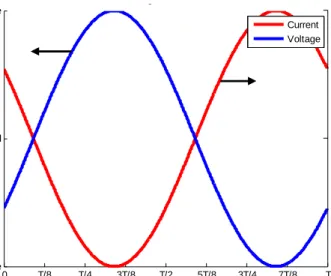
. The applied signal at the input is sinusoidal and the output network has a filter to pass the fundamental (could be matching network), and high pass filter to ground for the harmonics. In consequence for this, the drain current and voltage waveforms are sinusoidal.Since the transistor is on during all the cycle, the maximum efficiency is 50% for the ideal case. This efficiency number, in practice, is reduced significantly to about 35% for L band (i.e.; 1-2 GHz) applications. The ideal drain current and voltage waveforms for a
+ Vo - VDD Output Filter 180o 0o (a) (a) + Vo -+ VDS Output Filter VDD IDS DC -Feeder
0 T/8 T/4 3T/8 T/2 5T/8 3T/4 7T/8 T Vknee Vdd 2Vdd-Vknee g Time V o lt age [ V ] Current Voltage 0 Iq Imax C u rr ent [ A ]
Figure 2-3: Class A power amplifier drain voltage and current waveforms. 2.3.1.2 Class B power amplifier
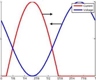
In class B the gate voltage is biased at the threshold to make the conduction angle equal to
π
, which increases the maximum theoretical efficiency from 50% in class A to 78.5% in class B. The ideal drain current and voltage waveforms for a class B power amplifier are sinusoidal because the drive input signal is sinusoidal and the output network has filters to pass the fundamental and to short out the harmonics, see Fig 2.4.0 T/8 T/4 3T/8 T/2 5T/8 3T/4 7T/8 T Vknee Vdd 2Vdd-Vknee Time V o lt age [ V ] g Current Voltage 0 Iq Imax C u rre n t [A ] 0 Iq Imax C u rre n t [A ]
Figure 2-4: Class B power amplifier drain voltage and current waveforms. 2.3.1.3 Class AB power amplifier
The class AB power amplifier is a state in between class A and class B, in which the gate is biased slightly above the threshold voltage to make the conduction angle between
CH2: Power Amplifier: Essentials and classes
the efficiency varies between 50% and 78.5%. The ideal drain current and voltage waveforms for a class AB power amplifier are shown in Fig. 2.5 (the sinusoidal shape occurs when the load is assumed to act as an ideal short circuit i.e.; zero resistance, for the harmonics). 0 T/8 T/4 3T/8 T/2 5T/8 3T/4 7T/8 T Vknee Vdd 2Vdd-Vknee Time V o lt ag e [ V ] g Current Voltage 0 Iq Imax C u rrent [ A ] 0 Iq Imax C u rrent [ A ] 0 Iq Imax C u rrent [ A ]
Figure 2-5: Class AB power amplifier drain voltage and current waveforms.
0 T/8 T/4 3T/8 T/2 5T/8 3T/4 7T/8 T Vknee Vdd 2Vdd-Vknee Time V o lt ag e [ V ] g Current Voltage 0 Iq Imax C u rre n t [A] 0 Iq Imax C u rre n t [A] 0 Iq Imax C u rre n t [A] 0 Iq Imax C u rre n t [A]
Figure 2-6: Class C power amplifier drain voltage and current waveforms. 2.3.1.4 Class C power amplifier
In class C, the biasing voltage is less than the threshold voltage. Hence, the conduction angle is less than that in class B (i.e.; less than
π
). The efficiency may reaches up to 100%. However, there are several problems for an (1-2 GHz) Class-C implementation. The first one is that the efficiency comes at the expense of the gain. In fact, the efficiency could reach 100% by reducing the conduction angle to zero. Unfortunately, this cause the output power to decrease toward zero and the drive input power to infinity. The seconddrawback is that the amplifier is highly nonlinear because it requires large drive input power, so it can be used only in applications that can tolerate a high degree of nonlinearity, or it has to be used with linearization techniques. The ideal drain current and voltage waveforms for a class C power amplifier are shown in Fig. 2.6.
Before we go to other classes, the next part shows simulation of an overdriven class AB power amplifier [15] with the effects of all the parasitic parameters from the device.
2.3.1.5 Overdriven class AB power amplifier simulated example
The device model used for this example has 100 mm gate width with including all the capacitances. For this amplifier, the load network was an ideal one in which the impedance value does not depend on the operating frequency. The operating frequency is
fo=1 GHz.
The circuit topology used in this example is shown in Fig. 2.7. (i.e.; single ended). The load network is a function of harmonic, see Equation 2.1 and the input source is one tone, its impedance is 1 Ω. ⎩ ⎨ ⎧ = = + = o o L 0 , , j f n f f f X R Z (2.1) ... 3 , 2 wheren=
To achieve the maximum efficiency, the load value should be adjusted to 6.4 Ω and inductive susceptance equal to -j0.141 S to tune out the effect of the output capacitance (i.e.; Cds), see Table 2.1 on page 13. The drain voltage is set as the default value (i.e.; Vdd=28 V). To make the conduction angle in the range of a class AB power amplifier, we need to have the gate voltage swinging above the threshold for more than the half period. Hence, it biased with gate voltage 3 V and input power level is equal to 25 dBm. The load line graph is shown in Fig 2.8.
Vout vggg P_1Tone PORT1 Freq=fc0 P=polar(dbmtow(Pin),phi) Z=1 Ohm {o} Num=1 DC_Feed DC_Feed1 V_DC Vgs Vdc=Vg V DC_Block DC_Block1 Y1P_Eqn Y1P1 Y[1,1]=j*yout Z1P_Eqn Z1P1 Z[1,1]=rout I_Probe I_out DC_Feed DC_Feed2 DC_Block DC_Block2 I_Probe I_dc V_DC Vdd Vdc=Vd V VAR VAR1 w=100 EqnVar I_Probe I_gs I_Probe I_Probe1 I_Probe I_ds GM8_simplified T1 alpha2=a cgd=Cgd cds=Cds cgs=Cgs repi=repi m=100/1.2 Cds Cgd Cgs Id
Figure 2-7: Circuit topology for class AB example.
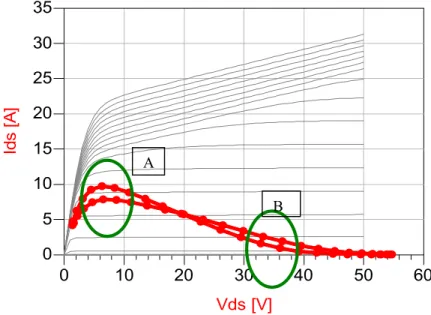
CH2: Power Amplifier: Essentials and classes 10 20 30 40 50 0 60 5 10 15 20 25 30 0 35 Vds [V] Id s [A ]
Figure 2-8: Overdriven class AB simulated load line.
As it can be seen from this graph the load line has small loops (i.e.; region A and B) which are probably due to two reasons. The first is that the load impedance still has some reactive value at the fundamental frequency, and the other is the feedback capacitor in the model (i.e.; Cgd)
which allows a leakage current passing from the input side to the output side.
The load line graph shows that the peak drain voltage is around 55 V (i.e.;2Vdd-VKnee) and the
minimum voltage is about 2 V (i.e.; the knee voltage) and it is swinging around drain bias voltage (i.e.; 28 V), the DC feeder has no losses. On the other hand, the current has peak value around 10 A.
The resultant current and voltage waveforms are shown in Fig. 2.9. The two current peaks are due to loop A in Fig. 2.8, and the asymmetry of the waveforms (rising and falling edges) is due to loop B in Fig. 2.8. The current waveform has one dip caused by the linear region in the I-V curve, this effect let us to call this class as an overdriven class AB [15].
The output load is shown in Fig 2.10 which has an impedance with almost zero imaginary part at the fundamental frequency and zero impedance at all the higher harmonics.
The results of this simulation (i.e.; output power, gain, and efficiency) are shown in Table 2.1.
Table 2-1: Numerical Values for Class AB
Bias and Load setup Results
RL [Ω] B1[S] Vg [V] Vdd [V] Pin [dBm] η [%] Pout [W] G [dB]
6.4 -0.141 3 28 25 53.5 55 19.5
A
0.2 0.4 0.6 0.8 1.0 1.2 1.4 1.6 1.8 0.0 2.0 10 20 30 40 50 0 60 2 4 6 8 10 0 12 t [ns] Id s [A ] MaxIds Vd s [ V ] MaxVds MinVds MaxVds time= ts(T1.vd)=54.67 V640.0psec MinVds time= ts(T1.vd)=1.314 V140.0psec MaxIds time= ts(T1.Id.i)=9.741 A1.240nsec
Figure 2-9: Voltage and Current Waveform for Class AB.
freq (1.000GHz to 5.000GHz) Z L [O hm ] F H F freq= Gload[1::5]=0.231 / 168.033 impedance = 6.285 + j0.637 1.000GHz H freq= Gload[1::5]=0.999 / 179.983 impedance = 0.007 + j0.001 3.000GHz
Figure 2-10: Load impedances for the first five harmonics. Comments
We could see that the efficiency is degrading from the maximum theoretical efficiency of an ideal class AB. The major reasons are: the conduction angle is larger than
π
, and the losses due to the knee region (Rds-on), overlapping waveforms due to the sinusoidalCH2: Power Amplifier: Essentials and classes
2.3.2 Switch mode power amplifiers
Switch mode power amplifiers (SMPAs) in all have a great advantage over previous classes in that they have 100% theoretical efficiency. They are called switch mode because the transistor is used like a switch instead of a linear current source as in the classes A, B, AB and C, and also because the current or the voltage waveforms have none sinusoidal shape.
Active devices can be modeled as a switch in two different ways, see Fig 2.11. Each model has its effect on the losses. In Fig. 2.11 (a), the losses are during the transition from off to on states, when the capacitor is discharged. On the other hand, in Fig. 2.11 (b), the losses are during the transition from on to off states, when the inductor is discharged. Both models need either zero voltage (across the switch) just before the switch is closed (i.e.; for the model in Fig 2.11. (a)) and this referred to zero voltage switching (ZVS), or zero current (through the switch) just before the switch is opened (i.e.; for the model in Fig 2.11. (b)) in this case it is referred to zero current switching (ZCS). Hence, one should take care of both transition states to reduce these losses as much as possible.
Figure 2-11: Transistor model as Switch.
The next sections are a give discussion of the switch mode power amplifiers.
2.3.2.1 Class D power amplifier
The class D power amplifier (or voltage mode class D VMCD) is the only class which requires two transistors working out of phase 180o. The circuit topology is shown in Fig.
2.12; the load network has a series resonant circuit to pass the current at the fundamental frequency to the load and to block all other current components. Hence the voltage and current waveforms are a square (odd component) and sinusoidal (even component) waveforms, respectively, see Fig. 2.13.
(b) (a) L C T R C T L R
Figure 2-12: Class D circuit topology. 0 T/2 T 3T/2 2T Vknee Vdd 2*Vdd-Vknee Time V o lt ag e [ V ] Current Voltage 0 Idmax/2 Idmax C u rr e n t [A ]
Figure 2-13: Class D voltage and current waveforms.
There is another class which is complementary to class D called D-1 (or current mode
class D CMCD). Its circuit topology could be as the circuit shown in Fig. 2.14. The class D-1 load network has a parallel resonant circuit with the load to pass the fundamental
frequency and to short the odd harmonics. This topology allows the current to have square waveform and the voltage sinusoidal waveform as shown in Fig. 2.15.
This class has an advantage over class D, in that it can tune out the transistor output capacitance, which comes from grounding the source in both transistors, and include it as a part of the resonant circuit. Therefore, we can still achieve high efficiency, but not 100% due to the knee region. Also, class D PA may exceed the breakdown voltage for T1
in Fig. 2.12 because its source terminal is not grounded
RL VDD + VDS IDS T1 T2 L C
CH2: Power Amplifier: Essentials and classes
Figure 2-14: Class D-1 circuit topology.
0 T/2 T 3T/2 2T Vknee 1.5*Vdd 3.14*Vdd Time V o lt a ge [ V ] Current Voltage 0 Idmax/2 Idmax Cu rre n t [ A ]
Figure 2-15: Class D-1 voltage and current waveforms.
Another reason of degrading the efficiency from the theoretical value is the transistor output capacitance which is significant at high frequency, is large due to the size required for the high output power application. The susceptance of the output capacitance is very high for the high frequency and cannot be ignored (i.e.; Y=jB=jωCds).
Also another reason of not achieving the theoretical efficiency is that the transistors do not work as ideal switches, which can be toggled between ON state and OFF state instantaneously. Within the finite turn-on and turn-off time, the voltage and the current overlap, and cause the transistor losses (switching loss). This drawback is addressed in the time domain design and analysis in Class E amplifiers.
2.3.2.2 Class E power amplifier
The typical circuit topology of class E power amplifier is shown in Fig. 2.16. The load network consists of series resonant circuit at the fundamental frequency and the
0o T 180o 1 L VDD R C T2
fundamental load tuned slightly inductive. This inductive load reduces the slope of the voltage waveform before the switch turns on. The ideal voltage and current waveforms for class E (assuming square drive signal) are shown in Fig 2.17.
Class E has two main advantageous:
1. Soft switching which reduces the losses.
2. Simple circuit topology compared to other switching classes.
However, class E has disadvantages in that the drain voltage has high peak value due to charging the large output capacitance, and the difficult to tune the output capacitance of the transistor. Additionally, to achieve ZVS condition, all the current must go through
Cds//Lout when the switch turn off. The current limit is set by I= jωCdsVds. Hence, the class
E has limit tolerance for large transistor output capacitance Cds that degrades the
maximum operating frequency performance.
Figure 2-16: Class E Circuit Topology.
0 T/2 T 3T/2 2T Vknee 1.8*Vdd 3.6*Vdd Time V o lt age [ V ] Current Voltage 0 Idmax/2 Idmax Cu rre n t [ A ]
Figure 2-17: Class E voltage and current waveforms.
+ Vds -VDD RL fo
CH2: Power Amplifier: Essentials and classes
VDD
2.3.2.3 Class F power amplifier
The class F power amplifier circuit is the most complex circuit among all the classes; it needs at least three resonators (to control up to the fifth harmonics) to short out even and to block the odd harmonics. The circuit topology is shown in Fig. 2.18. Class D is an ideal case for class F, in which the current is a sinusoidal waveform and the voltage is a square waveform.
Figure 2-18: Class F Circuit Topology.
As in class D, class F has a complementary circuit in which it blocks the even harmonics and short out the odd ones. This class called F-1 and it is circuit topology is shown in Fig.
2.19. This class has similar waveform as the ones in class D-1. However, this class needs
lower drain bias voltage than any other classes for the same output power (since the voltage waveform has higher peak than the square waveform i.e.; class F PA) and give high efficiency with lower peak voltage than class E. Hence, the breakdown voltage will not be exceeded in this class.
Figure 2-19: Class F-1 Circuit Topology.
RL + Vds -VDD RL f5 f3 fo fo + Vds -f2 f4
3 Class J power amplifier
In all the discussed switch mode classes there are some drawbacks for each one. Hence, one should find a compromise to achieve all the advantageous of the classes. Class J introduced recently in [15] combines the advantages of class E and F-1. However, this class
is introduced in some articles with different names but same operation like high frequency class E in [18] and class E/F in [19].
3.1 Theory of operation
The class J power amplifier requires a slightly inductive load at the fundamental frequency and only capacitive load at the second harmonic. The first requirement is similar to that one in the class E power amplifier. However, class J try to make fast switching transitions during the on and off state which reduces the losses and increases the efficiency, while in class E the on transition switching has less losses than the off transition switching (for sinusoidal drive signal).
On the other hand, class F-1 requires infinite number of resonators to achieve high
efficiency (but most of the work done by controlling up to the third harmonics), but class J requires one resonator (to control the first harmonic).
Like any other classes, class J power amplifier can be single ended or push-pull. In addition, it can be designed starting from any classic class of power amplifier.
3.2 Class J example
This example shows how to build class J PA starting from the example of class AB discussed before (i.e.; fo=1 GHz, single ended topology).
A class J design can be done in three steps (summarized from [15]) stated below: Step 1. Voltage peaking.
The first starting step is to use the previous example of class AB and try to block (ZL(2ωo)=∞) the second harmonic. The efficiency increased from 53% to 63%
(about 10 %!!), see Table 3.1. The table shows that the power increased about 10 Watt, the gain increases and the power loss is reduced about 10 Watt. This increment in the efficiency is because the transistor starts to act as a switch (the voltage waveform have higher second harmonic). Fig. 3.1 shows the waveforms for the current, voltage and instantaneous power between these cases, and Fig. 3.2 shows the voltage spectrum.
0.2 0.4 0.6 0.8 1.0 1.2 1.4 1.6 1.8 0.0 2.0 20 40 60 80 100 0 120 t [ns] Vd s [ V ]
Instantaneous Power Losse 0.2 0.4 0.6 0.8 1.0 1.2 1.4 1.6 1.8 0.0 2.0 2 4 6 8 0 10 t [ns] Id s [ A ] 0.2 0.4 0.6 0.8 1.0 1.2 1.4 1.6 1.8 0.0 2.0 20 40 60 0 80 t [ns] Vd [ V ] Voltage Waveforms Class AB Class AB blocking 2nd H Class AB Class AB blocking 2nd H Class AB Class AB blocking 2nd H
Figure 3-1: (a) Currents waveforms; (b) Voltage waveforms; (c) Instantaneous power waveforms for step 1.
(a) (c) (b) Inst_Pow er [ W ]
CH3: Class J Power Amplifier
Table 3-1: Numerical results for Class J steps
1.5 2.0 2.5 3.0 3.5 4.0 4.5 1.0 5.0 -40 -20 0 20 -60 40 Freq [GHz] Vd [ d B m ] Class AB Class AB blocking 2nd H
Figure 3-2: Voltage spectrum for step 1.
Step 2. Tune the fundamental inductively.
The next step directly is to try to tune the fundamental load slightly more inductive. Hence, high efficiency is achieved with same power in step 1. In Fig. 3.3 the first three harmonic loads are shown for this step and the previous one.
freq (1.000GHz to 3.000GHz) ZL [ O h m ] Fun Sec Third SecJ FunJ Fun freq= Gload[1::3]=0.240 / 165.323 impedance = 6.195 + j0.799 1.000GHz Sec freq= Gload[1::3]=1.804 / -93.834 impedance = -5.014 - j8.008 2.000GHz Third freq= Gload[1::3]=0.999 / 179.995 impedance = 0.033 + j0.002 3.000GHz SecJ freq= ABJ2..Gload[1::3]=0.894 / -114.953 impedance = 3.928 - j31.742 2.000GHz FunJ freq= ABJ2..Gload[1::3]=0.272 / 106.805 impedance = 37.588 + j21.164 1.000GHz
Figure 3-3: Load impedances for the first three harmonics.
Vpk [V] Pout [w] Gain [dB] η [%] Average Dissipated Power [w] Class AB 55 55.6 22.45 54.3 46.78 Voltage peaking 62 65.7 23.18 63 38.68 Inductive Tuning 74 65.5 23.16 70.54 26.15 Class J 77 55.6 17.5 86 7.40 [d BV]
This step gives different shape for the drain current and reduces the dissipated power, see Fig. 3.4. The peaks in the drain current don’t have the shape of the peaks in class AB or the peaks gotten from the previous step; this due to the load is inductive at the fundamental which makes the waveforms approach the ZVS condition. The numerical results are shown in Table. 3.1 on page 23 .
0.2 0.4 0.6 0.8 1.0 1.2 1.4 1.6 1.8 0.0 2.0 2 4 6 8 0 10 t [ns] Id s [ A ] 0.2 0.4 0.6 0.8 1.0 1.2 1.4 1.6 1.8 0.0 2.0 20 40 60 0 80 t [ns] Vd [ V ] Voltage Waveforms Class AB blocking 2nd H Inductive Load Class AB blocking 2nd H Class AB blocking 2nd H Inductive Load Inductive Load 0.2 0.4 0.6 0.8 1.0 1.2 1.4 1.6 1.8 0.0 2.0 50 0 100 t [ns] Vd s [ V ]
Instantaneous Power Losse
Figure 3-4: (a) Currents waveforms; (b) Voltage waveforms; (c) Instantaneous power waveforms for step 2.
Inst_Pow er [W ] (a) (c) (b)
CH3: Class J Power Amplifier
Step 3. Relative phasing – Class J
The last step is to try to adjust the relative phasing between the voltage and the current for the second harmonic (in another way, make the second harmonic load capacitive). In Table. 3.2, the phases for the first and the second harmonic for step two and step three are shown (∠Id- ∠Vd). However, the relative phasing is not purely capacitive for the second harmonic because the output capacitor for the transistor is not linear which degrades the desired +90o phase
difference. The fundamental load impedance has a high positive phase (not exactly -90o phase) and that is due to the real part is high compared to the
inductive part, see Fig. 3.5.
Table 3-2: Relative phases for all three steps.
Figure 3-5: The first three harmonics impedances. Relative Phase (
∠
Id-∠
Vd) [o]Harmonics
Class AB Blocking 2nd Hr Inductive Tuning Class J
Fundamental 0.21 -275 -20 -30 2nd -21 141.82 75.4 82 freq (1.000GHz to 3.000GHz) ZL [ O hm ] Fun Snd Fun freq= Gload[1::3]=0.389 / 90.806 impedance = 7.298 + j6.698 1.000GHz Snd freq= Gload[1::3]=0.947 / -124.450 impedance = 0.347 - j5.262 2.000GHz
Vd1 indep(Vd1)= vd[1]=39.183 / 135.0600 Id1 indep(Id1)= -Id.i[1]=3.329 / 105.0800 -30 -20 -10 0 10 20 30 -40 40 (0.000 to 0.000) V d [ V ], Id [ A ]. ( F unda m e nt a l) Vd1 Id1 Vd1 indep(Vd1)= vd[1]=39.183 / 135.0600 Id1 indep(Id1)= -Id.i[1]=3.329 / 105.0800 Vd2 indep(Vd2)= vd[2]=12.331 / -84.7430 Id2 indep(Id2)= -Id.i[2]=1.845 / -1.9970 -10 -5 0 5 10 -15 15 (0.000 to 0.000) V d [ V ], Id [ A ]. ( S e c ond ha rm oni c ) Vd2 Id2 Vd2 indep(Vd2)= vd[2]=12.331 / -84.7430 Id2 indep(Id2)= -Id.i[2]=1.845 / -1.9970 Id Vd
Figure 3-6: Phase graph for the drain voltage and current (a) fundamental, (b) 2nd harmonic.
In addition, two last modifications are done. The first is to reduce the gate bias voltage this allows the current to have a low dip value (i.e., knee region) and minimum voltage value during the ON/OFF-state, see Fig. 3.7 blue circles. The second modification is to increase the driving power to achieve high efficiency with the maximum output power rating, Table. 3.1 last raw on page 23. Fig. 3.8 (c), shows the instantaneous power loss. The dashed area is the reduction in the losses achieved by class J which is about 40 W (around 34%) loss reductions from class AB. However, the drain peak voltage increased from 55 V in class AB to 77 V in class J, and the gain reduced about 5 dB from the gain achieved in class AB.
CH3: Class J Power Amplifier 0.2 0.4 0.6 0.8 1.0 1.2 1.4 1.6 1.8 0.0 2.0 2 4 6 8 0 10 t [ns] Id s [ A ] Current Waveforms 0.2 0.4 0.6 0.8 1.0 1.2 1.4 1.6 1.8 0.0 2.0 20 40 60 0 80 t [ns] Vd [ V ] Voltage Waveforms Class J Class J Class AB inductive+2nd H Class AB inductive+2nd H
Figure 3-7: (a) Current Waveforms; (b) Voltage Waveforms for step 3.
Figure 3-8: Instantaneous power waveforms for step 3. (a)
Now, the class J design is complete and we can start analysis of its waveforms. The load line graph is shown in Fig. 3.9, and it can be seen that the voltage has the minimum value during the on-state which reduces the losses. Also, there is zero drain voltage at the dip of the current, which means no lost power, see Fig. 3.10. However, the waveforms look like class E and F-1!
10
20
30
40
50
60
70
0
80
2
4
6
8
10
0
12
Vd [V]
Id
[
A
]
Load Line Graph
Figure 3-9: Load line for class J.
Vmax time= ts(vd)=77.09 V580.0psec Imax time= ts(Id.i)=8.422 A260.0psec 0.2 0.4 0.6 0.8 1.0 1.2 1.4 1.6 1.8 0.0 2.0 10 20 30 40 50 60 70 0 80 1 2 3 4 5 6 7 8 0 9 t [ns] Vd [V], Inst_ P ow er [W] Vmax Id [A] Imax
Current, Voltage, & Instantaneous Power Waveforms
Vmax time= ts(vd)=77.09 V580.0psec Imax time= ts(Id.i)=8.422 A260.0psec Voltage Current Inst_Power
CH3: Class J Power Amplifier
3.3 Class J comparison with class E and F -1
The comparison will be taken in three different steps stated below. The circuit topologies for class E and class F-1 is the same as the circuit shown in Fig 2.7 on page 12. The bias
setup and drive input power values are shown in Table 3.3 on page 32. The concern was to compare these classes with class J for the same output power and same gate bias voltage.
3.3.1 Load line comparison
The load lines of class J and F-1 are shown in Fig. 3.11. Class J has lower dip and bigger
loop at the knee region comparing to F-1. On the other hand, class J and E load lines are
shown in Fig. 3.12. Class J has smaller loop at the knee region, but not zero drain voltage during turn on-state, on the contrary to class E (i.e.; ZVS). However, class E has higher losses in the turn off-state (i.e.; since we are assuming sinusoidal gate drive instead of rectangular). Hence, class J is a trade off in losses between the on-transition and the off-transition. 10 20 30 40 50 60 70 0 80 0 2 4 6 8 10 12 -2 14 Vd [V] Id [ A ] Class J Class Finv
Figure 3-11: Class J and class F-1 load line.
0 10 20 30 40 50 60 70 80 -10 90 0 2 4 6 8 10 12 -2 14 Vd [V] Id [ A ] Class J Class E
3.3.2 Voltage and current waveforms
The current waveforms for class J, class E and class F-1 are shown in Fig. 3.13 (a). Class
F-1 has a symmetrical current waveform which is almost square shaped (if the infinite
harmonics are controlled). Class E has longer OFF-state and higher peak current. On the other hand, class J has two peaks and one dip (unlike class F-1 which is symmetrical). For
the voltages in each class we can find that class J is a middle case in the peak value with respect to class E and class F-1, see Fig 3.13 (b).
0.2 0.4 0.6 0.8 1.0 1.2 1.4 1.6 1.8
0.0
2.0
0
2
4
6
8
10
-2
12
t [ns]
Id
s [
A
]
0.2 0.4 0.6 0.8 1.0 1.2 1.4 1.6 1.8
0.0
2.0
10
20
30
40
50
60
70
80
0
90
t [ns]
Vd
[
V
]
Voltage Waveforms
Class J
Class E
Class Finv
Class J
Class E
Class Finv
Figure 3-13: Class J, class E and class F-1, (a) Current and (b) Voltage waveforms.
(a)
CH3: Class J Power Amplifier
3.3.3 Losses in the three classes
It is worth to look at the losses in each of the three classes, see Fig. 3.14 and Table 3.3. The blue dashed area in Fig. 3.14 is the reduction in loss in class J with respect to class E and F-1 while the black dashed area is the increment loss. It is clear from these dashed
areas that class J has less loss than class E while almost the same loss as class F-1, see
Table 3.3.
Figure 3-14: Instantaneous power waveforms (a) between class J and class E (b) between
class J class and F-1.
(a)
Table 3-3: Numerical comparisons for class E, class J and class F-1.
*: All the classes designed for 50 W output power and more than 12 dB gain
3.4 Class J Pros. and Cons.
One can recognize some advantages of class J which motivate to choose it as a good approach for high efficiency. Table. 3.4 summarize the main pros and cons of class J with respect to class E and F-1.
Table 3-4: Comparison between class E, class J and class F-1.
*: The comparison for class F−1 when controlling 5 harmonics
It can be concluded from Table. 3.4, class J is a trade off between class E and class F-1
and easier to implement that class F-1, which motivate the research to take class J as a
base-stone of the design strategy.
Circuit setup Results
Classes* Vdd [V] Vgs [V] Pin [dBm] ZL [V] Vd(fo) [V] Vd(2fo) [V] Id(fo) [A] Id(2fo)/ Id(3fo) [A] Vpk [V] Vpk/Vdd [V] Pdc [W] η [%] G [dB] Losses [W] E 28 2.56 30 7.3 +j6.6 41.7 18.5 4.5 2.7 90 3.2 84 80.3 18.3 16.7 F-1 21 2.57 35 7.8 +j2.9 30.7 12.4 3.5 0.72 62 3 60 87.5 12.2 6.6 J 28 2.5 30 7.3 +j6.6 39.2 12.3 3.3 1.9/ 1.3 77 2.8 64.7 86 817.5 7.4 E J F-1 Circuit topology
Easy (i.e.; need one resonator) and could be
single ended or push-pull
Easy (i.e.; need one resonator) and could be single ended or
push-pull
Very complex (i.e.; need at least 5 resonator to achieve high efficiency)
Peak voltage Very high
Lower than class E and higher than class
F-1
Low (i.e.; Doesn’t exceed the break down voltage)*
Losses adjust ZVS condition) Highest losses (i.e.;
Small losses (i.e.; trade off between OFF and ON-state
transition )
Almost like class J losses
4 Design
strategy
This chapter will describe in detail the design strategy; including the circuit model, and the bondwire model.
It is obvious now from pervious chapters that any type of SMPA needs a resonator circuit(s) to perform the waveform shaping. Class J PA requires one resonator to give an inductive load for the fundamental and a capacitive load of appropriate size for the second harmonic. Before we discuss the schematic, we should decide if either of the single-ended or push-pull topologies should be used.
4.1 Single-ended and push-pull
4.1.1 Push-pull
A push-pull amplifier consists of an input 0o-180o power splitter driving two identical
devices in anti-phase and an 180o-0o output power combiner adding the output power of
the two devices in the amplifier load. These types of splitters/combiners, which are key elements of the amplifier, are called BALUNS (BALanced to Unbalanced transformer). They transform a balanced system that is symmetrical (equal in magnitude and opposite in sign) with respect to ground to an unbalanced system with one grounded terminal. Note that the microwave push- pull amplifier consists of two devices, each contributing half the total power. Fig. 2.2 on page 9shows the circuit topology.
4.1.2 Single-ended
The single-ended topology (see Fig. 2.2) uses one power amplifier. It doesn't need a splitter at the input side, or a combiner at the output side which reduces the complexity and loss of the circuits.
4.1.3 Advantages of single-ended push-pull topology
Table 4.1 shows the advantages and disadvantages of the single-ended and push-pull power amplifiers.
Table 4-1: comparison between Single-ended and push-pull.
Comparisons points Push-Pull Single-Ended
Output Power and matching impedance
Lower impedance ratio (for double the impedance ratio the output power is same as single ended; while for four times higher impedance ratio, the output power is double of the
single ended).
-
Bandwidth Higher BW due to the lower
impedance ratio. Lower BW.
Harmonic termination
The output current (i.e.; balanced load current) doesn't
contain even harmonics [21].
The output currents contains all the harmonics
Voltage peaking without
2nd harmonic resonator
Can use the output capacitance in the resonator for class J
Need either small Cds like
GaN, or 2nd harmonic
resonator to tune Cds.
complexity
More complex since it requires two transistors and input/output BALUNs
Simple circuit topology (requires one transistor and
normal input/output matching network)
Total Efficiency Lower; since it uses balun for
the output. higher
Push-pull topology gives a wider bandwidth, even harmonics filtering and could use the output capacitance in the resonator. Hence, it is a good topology choice for class J (taking in consideration to design low loss balun).
4.2 Idea
The goal of the project now is to build a one stage push-pull PA with maximum drain efficiency and high gain at 2.14 GHz. The resonator is integrated inside the package using the bondwire and capacitances. Several baluns will be studied to figure out a low loss circuit compatible with the design. The input output PCB (printed circuit board) matching networks will be designed for 50Ω SMA connectors.
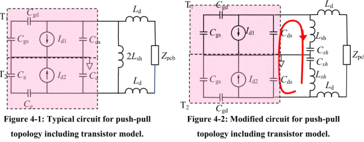
CH4: Design Strategy Ld Zpcb Id1 Cgs Cgd Cds Id2 Cg Cg Cd 2Lsh Ld T1
4.3 Circuit design and analysis
Designing a push-pull class J requires a parallel resonator to tune the output capacitance
Cds. The most straight forward topology is the one shown in Fig. 2.3 or Fig. 4.1. In this topology Cds is used as a part of the resonator. The circuit can be modified by dividing the
shunt inductance, as it is shown in Fig. 4.2, for practical implementation inside the package using bondwires. The capacitors Csh are necessary to block the DC-current
components.
Figure 4-1: Typical circuit for push-pull topology including transistor model.
Figure 4-2: Modified circuit for push-pull topology including transistor model.
The resonant current at the fundamental is the red path shown in Fig. 4.2. Moreover, the differential load branch (Zpcb+jωLd) is invisible at the even harmonics due to the push pull
operation. Hence, it satisfies the second harmonic condition for class J (i.e.; capacitive load which is Cds, assuming Ish(2fo)
≈
0).There are different types of resonators, each has different properties. The choice of the resonator shown in Fig 4.2 is due to practical implementation. It can be open at the fundamental (i.e.; Cds is not seen from the transistor). Equation 4.1 helps to find the
inductive value for Lsh. However, one may optimize this value to get the impedance level
that achieves high efficiency with maximum gain rating.
sh ds 2 ds sh sh -C C C C L
ω
= (4.1)Finally, this circuit topology can be done either with discrete component or integrated inside the package. The second choice could give further development to integrate the in/out balun, and to use the integrated resonator on silicon substrate (i.e.; P7MI technology). Moreover, it is easier to build this circuit integrated inside the package with currently available tools, which still gives high efficiency in the simulator. Hence, Fig 4.2 is the motivated one for this work.
T2 T1 Id1 Zpc b Ld Ld Lsh Csh Lsh Csh Cds Cds Cgs Cgs Cgd Id2 Cgd T2 Zpcb o
4.4 Input matching circuit
The complete circuit of the package device with internal matching network is shown in Fig 4.3. The input side includes two sections of low pass filter circuit to give a wider bandwidth than a single section circuit since the impedance ratio per section is lower than for the single section case. The design formula for matching network can be found in [15] or [16]. Also it includes the pad capacitances for the input and output leads Cpg and Cpd,
respectively.
Figure 4-3: Full circuit model of the IC.
4.5 Bondwire: theory and design
Bondwires are used to connect any semiconductor device to the output world. For low frequency the bondwire parasitics are negligible. However, at high frequency (i.e.; microwave frequency) the bondwire parasitic cannot be neglected. A typical bondwire model valid at high frequency is shown in Fig. 4.4. It is constructed from inductance and series resistance with shunt capacitance on both sides. A typical inductive value is 1 nH/mm length of bondwire. However, the inductance does not reduce linearly with the number of parallel bondwires, due to the mutual inductive coupling between the bondwires, see Fig. 4.5. On the other hand, the capacitance increases linearly with the number of bondwires, but usually it is neglected for small number of bond-wires at low GHz frequency, because the surface area of the bond-wires is small.
Figure 4-4: Bond-wire, with its circuit model.
Ld Id1 Cgs Cgd Cds Id2 Cgs Cgd Cds Lsh Ld Lsh Csh Csh Cpd Cpd L1 C1 C1 L2 L L Cpg Cpg
CH4: Design Strategy
The bond-wire inductance can be calculated analytically or by simulation. The latter one is used here because the bond-wire inductance in the resonator circuit is relatively small; hence, the number of bond-wires will be large, which makes the analytical calculation difficult. The simulation is done using Agilent ADS, Philips/Delft model [21]. This model calculates the bond-wire inductance and mutual inductance between each set of bond-wires. Also, it calculates the DC-resistance and AC-resistance. However, the substrate losses are not included with this model, which reduces the quality factor compared to what can be calculated from the model (i.e.; Q=
ω
L R). The model does not calculate the coupling capacitance between the bondwires and the coupling capacitance between the bond-wires and the ground plane. Moreover, it does not calculate the radiation losses, and neglect the current distribution due to the proximity effect (i.e.; when two or more bondwires are located very close to each other) [21].The self-inductances and mutual-inductances of the bond-wires are designed and included in the circuit model for all bond-wire sets, see appendix B page 75 and 76.
2 4 6 8 10 12 0 14 0.4 0.6 0.8 1.0 1.2 0.2 1.4 No. of Bond-Wires L [ n H ]
5 IN/OUT- PCB design
The IN-PCB (i.e.; BALUN, input matching and the DC-feeder) is critical for the input impedance matching to achieve high gain, which in turn would mean the PAE will be almost equal to the drain efficiency. The OUT-PCB is important to obtain the correct load line giving high efficiency and the maximum power. Both parts (IN/OUT-PCB) contain three sub networks; BALUN, matching network and DC-bias, see Fig 5.1. The transistor package sub circuit is shown in Fig 4.3 on page 36. The topologies used for IN-PCB network and OUT-PCB network are same. Also, the four DC-Bias networks have the same topology.
Figure 5-1: Design Blocks.
5.1 BALUN Design
The BALUN is a three port device that splits the signal into two equal signals but with 180o difference in phase. However, it can also combine two signals which are 180o out of
phase. Before we go for the topologies discussion, it is good to discuss the impact of two signals which are different in phase or in magnitude [22]. Fig 5.2 shows the typical push-pull amplifier with IN/OUT BALUN.
DC-Gate
Bias DC-Drain Bias
DC-Gate
Bias DC-Drain Bias
BALUN Matching IN- Matching OUT- BALUN
Zload=50 Ω
Pin
Zo=50 Ω
Packaged push-pull
Figure 5-2: Push-Pull topology with BALUN.
First let us find the output voltage when there is no phase or amplitude imbalance. Assume ) cos( 1 A t V =
ω
, and ) cos( 2 A t V =ω
are inputs for the balance ports of the BALUN. Hence, the output is:
) cos( ) cos( out A ωt A ωt V = + ) cos( 2 out A ωt V = (5.1)
Equation 5.1 represents the ideal output voltage from the BALUN. 1. Let us take the phase imbalance case:
Assume ) cos( 1 A ωt V = , and ) ∆ cos( 2 A ωt Φ V = +
are inputs for the balance ports of the BALUN. Hence, the output is:
) cos( ) cos( out A ωt A ωt Φ V = + +∆
[
cos( ) cos( )]
out A ωt ωt Φ V = + +∆ ) 2 )cos( 2 2 cos( 2 out Φ Φ ωt A V = +∆ ∆ (5.2)Hence comparing equation 5.2 with equation 5.1, the loss1 will be:
2 loss cos( 2 )⎥⎦ ⎤ ⎢⎣ ⎡ ∆ = Φ P (5.3)
1 The imbalance in phase or/and in amplitude lead to mismatch which may result in nonideal
180o 0o 0o 180o OUT V2o V1i V2i V1o IN - imbalance P out, V imbalance P out, V imbalance P out, V P L
CH5: IN/OUT-PCB Design
2. Next, the amplitude imbalance case:
) cos( 1 1 A ωt V = , and ) cos( 2 2 A ωt V =
are inputs for the balance ports of the BALUN. Hence, the output is:
) cos( ) cos( 2 1 out A ωt A ωt V = +
[
1 2]
cos( ) out A A ωt V = +[
1 2 1]
cos( ) 1 out A A A ωt V = + (5.4)comparing equation 5.4 with equation 5.1, the loss will be:
For microwave frequencies it is difficult to measure the amplitude of a signal, hence, equation 5.3 and 5.5 could be converted to S-parameters for simplicity during the simulation and the measurements.
From [10] S-parameters could be calculated by:
j K for V j i ij k V V S ≠ = + − + = 0 (5.6)
where positive sign and negative sign represent the incident and the reflected waves. For the phase difference
)) ( phase ) ( phase ( abs 180− S31 − S21 = ∆Φ (5.7)
where, port 1 represent the unbalanced port, and port 2 and port 3 represent the balanced ports.
For the amplitude ratio
21 31 1
2/A S /S
A = (5.7)
Now we can use equation 5.3 and 5.5 with the new values of
∆Φ
andA2/ A1.Fig 5.3 and Fig 5.4, show the power loss represented in equation 5.3 & equation 5.5, respectively. The power loss due to the phase imbalance can be neglected for more than 5o. On the other hand, power loss due to the amplitude imbalance is critical even for small
imbalance amplitudes. Hence, the design should consider the amplitude balance as an important issue.