5
th
FPGAworld
SEPTEMBER 11
STOCKHOLM, SWEDEN
Lennart Lindh
ACADEMIC
The FPGAworld Conference addresses all aspects of digital and hardware/software system engineering on FPGA technology.
engineers working on industrial and research projects, state development and applications.
report contain also the industrial presentations (www.fpgaworld.com/conference
FPGAworld CONFERENCE
SEPTEMBER 11
STOCKHOLM, SWEDEN
EDITORS
Lennart Lindh, Vincent J. Mooney III and Santiago de Pablo
ACADEMIC PROCEEDINGS 2008
The FPGAworld Conference addresses all aspects of digital and hardware/software system engineering on FPGA technology. It is a discussion and network forum for researchers and engineers working on industrial and research projects,The proceedings contain the academic presentations report contain also the industrial presentations; for more information
www.fpgaworld.com/conference). ISBN 978-91-976844-0-8
SPONSORS
CONFERENCE
STOCKHOLM, SWEDEN
and Santiago de Pablo
ROCEEDINGS 2008
The FPGAworld Conference addresses all aspects of digital and hardware/software systemIt is a discussion and network forum for researchers and -art investigations, the academic presentations a separate more information see
4th FPGAworld CONFERENCE, Lennart Lindh, Vincent John Mooney III (external), MRTC report ISSN 1404-3041 ISRN MDH-MRTC-215/2007-1-SE, Mälardalen Real-Time Research Centre, Mälardalen University, September, 2007
3rd FPGAworld CONFERENCE, Lennart Lindh, Vincent John Mooney III (external), MRTC report ISSN 1404-3041 ISRN MDH-MRTC-204/2006-1-SE, Mälardalen Real-Time Research Centre, Mälardalen University, November, 2006
2nd FPGAworld CONFERENCE, Lennart Lindh, Vincent John Mooney III (external), MRTC report ISSN 1404-3041 ISRN MDH-MRTC-188/2005-1-SE, Mälardalen Real-Time Research Centre, Mälardalen University, September, 2005
Copyright and Reprint Permission for personal or classroom use are allowed with credit to FPGAworld.com. For commercial or other for-profit/for-commercial-advantage uses, prior permission must be obtained from FPGAworld.com.
Additional copies of 2008 or prior Proceedings may be found at www.FPGAworld.com or at Jönköpings University library (www.jth.hj.se), ISBN 978-91-976844-0-8
2008 PROGRAM COMMITTEE
General Chair
Lennart Lindh, FPGAworld, Sweden
Publicity Chair
David Kallberg, FPGAworld, Sweden
Academic Programme Chair
Vincent J. Mooney III, Georgia Institute of Technology, USA
Academic Publicity Chair
Santiago de Pablo, University of Valladolid, Spain
Academic Programme Committee Members
Ketil Roed, Bergen University College, Norway
Lennart Lindh, Jönköping University, Sweden
Pramote Kuacharoen, National Institute of Development Administration, Thailand
Mohammed Yakoob Siyal, Nanyang Technological University, USA
Fumin Zhang, Georgia Institute of Technology, USA
Santiago de Pablo, University of Valladolid, Spain
General Chair
The FPGAworld program committee
conference. This year’s conference is held
We hope that the conference
expected. This year it
papers; this is an important step to
into the conference program.
papers submitted this year were
We will try to balance academic and industrial presentations
exhibits and tutorials to provide a unique chance f
obtain knowledge from different views
program in FPGAworld´s
The FPGAworld 2008
conference. Totally we are close to 300 participants (Stockholm and Lund).
All are welcome to submit
tutorials to the conference
backgrounds. Together we can make the
even above our best expectations
Please check out the website (http://fpgaworld.com/conference/)
more information about FPGAworld 2008
David Källberg (
david@fpgaworld.com
We would like to thank all of the authors for submitting their papers and
hope that the attendees enjoyed the FPGAworld conf
welcome to next year’s conference in 2009 in September.
Lennart Lindh
General Program Chair
General Chairman’s Message
program committee welcomes you to the
. This year’s conference is held in Electrum-Kista, Stockholm.
conferences provide you with much more then you
it is the fourth time we have acad
is an important step to incorporate the academic community
the conference program. Due to the high quality, 5
this year were presented.
to balance academic and industrial presentations
to provide a unique chance for our attendants to
from different views. This year we have the strongest
´s history.
conference is bigger than the FPGAworld
Totally we are close to 300 participants (Stockholm and Lund).
elcome to submit industrial/academic papers, exhibits and
to the conference, both from student, academic and industrial
Together we can make the FPGAworld conference exceed
expectations!
check out the website (http://fpgaworld.com/conference/)
information about FPGAworld 2008. In addition, you may contact
david@fpgaworld.com
) for more information
We would like to thank all of the authors for submitting their papers and
hope that the attendees enjoyed the FPGAworld conference 2008 and you
welcome to next year’s conference in 2009 in September.
man’s Message
you to the 5
thFPGAworld
Kista, Stockholm.
you with much more then you
time we have academic reviewed
incorporate the academic community
he high quality, 5 out of the 17
to balance academic and industrial presentations (Stockholm),
r our attendants to
e the strongest
n the FPGAworld 2007
Totally we are close to 300 participants (Stockholm and Lund).
, exhibits and
academic and industrial
conference exceed
check out the website (http://fpgaworld.com/conference/) for
. In addition, you may contact
for more information.
We would like to thank all of the authors for submitting their papers and
erence 2008 and you
Contents
Sessions B1-B4: Methodologies for FPGA design ...
§ A Java-Based System for FPGA Programming ...
§ Automated Design Approach for On-Chip Multiprocessor Systems
§ ASM++ charts: an Intuitive Circuit Representation
Ranging from Low Level RTL to SoC Design ...
Sessions B5-B7:
Custom Hardware Modules for FPGAs ...
§ Space-Efficient FPGA-Implementations of FFTs
in High-Speed Applications ...
§ The ABB NoC - a Deflective Routing 2x2 Mesh NoC
A Java-Based System for FPGA Programming
Jacob A. Bower, James Huggett, Oliver Pell and Michael J. Flynn
Maxeler Technologies
{jacob, jhuggett, oliver, flynn}@maxeler.com
Abstract
Photon is a Java-based tool for programming FPGAs. Our objective is to bridge the gap between the ever in-creasing sizes of FPGAs and the tools used to program them. Photon’s primary goal is to allow rapid develop-ment of FPGA hardware. In this paper we present Photon by discussing both Photon’s abstract programming model which separates computation and data I/O, and by giving an overview of the compiler’s internal operation, includ-ing a flexible plug-and-play optimization system. We show that designs created with Photon always lead to deeply-pipelined hardware implementations, and present a case study showing how a floating-point convolution filter de-sign can be created and automatically optimized. Our final design runs at 250MHz on a Xilinx Virtex5 FPGA and has a data processing rate of 1 gigabyte per second.
1. Introduction
Traditional HDLs such as VHDL or Verilog incur major development overheads when implementing circuits, par-ticularly for FPGA which would support fast design cycles compared to ASIC development. While tools such as C-to-gates compilers can help, often existing software cannot be automatically transformed into high-performance FPGA designs without major re-factoring.
In order to bridge the FPGA programming gap we pro-pose a tool called Photon. Our goal with Photon is to sim-plify programming FPGAs with high-performance data-centric designs.
Currently the main features of Photon can be summa-rized as follows:
• Development of designs using a high-level approach combining Java and an integrated expression parser. • Designs can include an arbitrary mix of fixed and
floating point arithmetic with varied precision. • Plug-and-play optimizations enabling design tuning
without disturbing algorithmic code.
• VHDL generation to enable optimizations via conven-tional synthesis tools.
• Automation and management of bitstream generation for FPGAs, such as invoking FPGA vendor synthesis tools and simulators.
The remainder of this paper is divided as up as follows: In Section 2, we compare Photon and other tools for creat-ing FPGA designs. In Section 3 we describe Photon’s pro-gramming model which ensures designs often lead to high-performing FPGA implementations. In Sections 4 and 5 we give an overview of how Photon works internally and present a case study. Finally, in Section 6 we summarize our work and present our conclusions on Photon so far.
2. Comparisons to Other Work
In Table 1 we compare tools for creating FPGA designs using the following metrics:
• Design input – Programming language used to create designs.
• High level optimizations – Automatic inference and optimizing computation hardware, simplification of arithmetic expressions etc.
• Low level optimizations – Boolean expression min-imisation, state-machine optimizations, eliminating unused hardware etc.
• Floating-point support – Whether the tool has intrinsic support for floating-point and IEEE compliance. • Meta-programmability – Ability to statically
meta-program with weaker features being conditional com-pilation and variable bit-widths and stronger features such as higher-order design generation.
VHDL and Verilog use a traditional combination of structural constructs and RTL to specify designs. These tools typically require a high development effort. Such con-ventional tools typically have no direct support for floating
Photon Impulse-C Handel-C Verilog VHDL PamDC JHDL YAHDL ASC
Design input Java C C Verilog VHDL C++ Java Ruby C++
Floating-point IEEE IEEE No No No No No No Yes
High-level Yes Yes Yes No No No No No No
optimizations
Low-level Via Via Yes Yes Yes No No No No
optimizations VHDL HDL
Meta-programmability Strong Weak Medium Medium Medium Strong Strong Strong Strong
Build automation Yes Yes Limited No No No No Yes No
Table 1. Comparison of tools for creating FPGA designs from software code.
point arithmetic and therefore require external IP. Meta-programmability e.g. generics in VHDL are fairly inflexi-ble [1]. The advantage of VHDL and Verilog is that they give the developer control over every aspect of the micro-architecture, providing the highest potential for an optimal design. Additionally, synthesis technology is relatively ma-ture and the low-level optimizations can be very effective. Other tools often produce VHDL or Verilog to leverage the low-level optimizers present in the conventional synthesis tool-chain.
Impulse-C [2] and Handel-C [3] are examples of C-to-gates tools aiming to enable hardware designs using lan-guages resembling C. The advantage of this approach is existing software code can form a basis for generating hard-ware with features such as ROMs, RAMs and floating-point units automatically inferred. However, software code will typically require modifications to support a particular C-to-gates compiler’s programming model. For example explicitly specifying parallelism, guiding resource map-ping, and eliminating features such as recursive function calls. The disadvantage of C-to-gates compilers is that the level of modification or guidance required of a developer may be large as in general it is not possible to infer a high-performance FPGA design from a C program. This arises as C programs in general are designed without parallelism in mind and are highly sequential in nature. Also, meta-programmability is often limited to the C pre-processor as there is no other way to distinguish between static and dy-namic program control in C.
PamDC [4], JHDL [5], YAHDL [1] and ASC [6] are examples of Domain Specific Embedded Languages [7] (DSELs) in which regular software code is used to imple-ment circuit designs. With this approach all functionality to produce hardware is encapsulated in software libraries with no need for a special compiler. These systems are a purely meta-programmed approach to generating hardware with the result of executing a program being a net-list or HDL for synthesis. Of these systems, PamDC, JHDL and YAHDL all provide similar functions for creating hardware
structurally in C++, Java and Ruby respectively. YAHDL and PamDC both take advantage of operator overloading to keep designs concise, whereas JHDL designs are often more verbose. YAHDL also provides functions for au-tomating build processes and integrating with existing IP and external IP generating tools. ASC is a system built on top of PamDC and uses operator overloading to spec-ify arithmetic computation cores with floating-point opera-tions.
Photon is also implemented as a DSEL in Java. Photon’s underlying hardware generation and build system is based on YAHDL rewritten in Java to improve robustness. Un-like JHDL, Photon minimizes verbosity by using an inte-grated expression parser which can be invoked from regular Java code. Photon also provides a pluggable optimization system unlike the other DSELs presented, which generate hardware in a purely syntax directed fashion.
3. Photon Programming Model
Our goal with Photon is to find a way to bridge the grow-ing FPGA size versus programmgrow-ing gap when accelerat-ing software applications. In this section we discuss the programming model employed by Photon which provides high-performance FPGA designs.
FPGA designs with the highest performance are gen-erally those which implement deep, hazard free pipelines. However, in general software code written without par-allelism in mind tends to have loops with dependen-cies which cannot directly be translated into hazard free pipelines. As such, software algorithm implementations often need to be re-factored to be amenable to a high-performance FPGA implementation. Photon’s program-ming model is built around making it easy to implement suitably re-factored algorithms.
When developing our programming model for Photon, we observe that dense computation often involves a sin-gle arithmetic kernel nested in one or more long running loops. Typically, dense computation arises from
repeat-ing the main kernel because the loop passes over a very large set of data, or because a small set of data is being iter-ated over repeiter-atedly. Examples of these two cases include convolution, in which a DSP operation is performed on a large set of data [8], and Monte-Carlo simulations repeat-edly running random-walks in financial computations [9].
In the Photon programming model we implement ap-plications following this loop-nested kernel pattern by di-viding the FPGA implementation into two separate design problems:
1. Creating an arithmetic data-path for the computation kernel.
2. Orchestrating the data I/O for this kernel.
Thus, we turn organizing data I/O for the kernel into a problem that can be tackled separately from the data-path compiler. Thus this leaves us with an arithmetic kernel which does not contain any loop structures and hence can be implemented as a loop-dependency free pipeline.
In Photon we assume the Data I/O problem is solved by Photon-external logic. Based on this assumption, Photon designs are implemented as directed acyclic graphs (DAGs) of computation. The acyclic nature of these graphs ensures a design can always be compiled to a loop-dependency free pipeline.
Within a Photon DAG there are broadly five classes of node:
• I/O nodes – Through which data flows into and out of the kernel under the control of external logic.
• Value nodes – Nodes which produce a constant value during computation. Values may be hard-coded or set via an I/O side-channel when computation is not run-ning.
• Computation nodes – Operations including: arith-metic (+, ÷ . . . ), bit-wise (&, or, . . . ), type-casts etc. • Control nodes – Flow-control and stateful elements,
e.g.: muxes, counters, accumulators etc.
• Stream shifts – Pseudo operations used to infer buffer-ing for simulatbuffer-ing accessbuffer-ing to data ahead or behind the current in-flow of data.
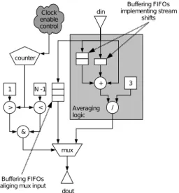
To illustrate Photon’s usage and graph elements, con-sider the pseudo-code program in Listing 1. This program implements a simple 1D averaging filter passing over data in an array din with output to array dout. The data I/O for this example is trivial: data in the array din should be passed linearly into a kernel implementing the average fil-ter which outputs linearly into an array dout.
f o r i i n 0 t o N do i f i > 1 and i < N−1 t h e n d o u t [ i ] = ( d i n [ i ] + d i n [ i −1]+ d i n [ i + 1 ] ) / 3 e l s e d o u t [ i ] = d i n [ i ] end end
Listing 1. Pseudo-code 1D averaging filter.
Figure 1. Photon DAG for 1D averaging.
Figure 1 shows a Photon DAG implementing the aver-aging kernel from Listing 1. Exploring this graph from top-down: data flows into the graph through the din input node, from here data either goes into logic implementing an av-eraging computation or to a mux. The mux selects whether the current input data point should skip the averaging op-eration and go straight to the output as should be the case at the edges of the input data. The mux is controlled by logic which determines whether we are at the edges of the stream. The edge of the stream is detected using a com-bination of predicate operators (<, >, &) and a counter which increases once for each item of data which enters the stream. The constant input N − 1 to the < comparator can be implemented as a simple constant value, meaning the size of data which can be processed is fixed at com-pilation time. On the other hand, the constant input can be implemented as a more advanced value-node that can be modified via a side-channel before computation begins, thus allowing data-streams of any size to processed. The logic that performs the averaging computation contains a number of arithmetic operators, a constant and two stream-shifts. The stream-shift operators cause data to be buffered such that it arrives at the addition operator one data-point behind (−1) or one data-point ahead (+1) of the unshifted
Figure 2. Scheduled DAG for 1D average filter.
data which comes directly from din.
To implement our 1D averaging Photon DAG in ware, the design undergoes processing to arrive at a hard-ware implementation. Figure 2 illustrates the result of Pho-ton processing our original DAG. In this processed DAG, buffering implements the stream-shifting operators and en-sures data input streams to DAG nodes are aligned. Clock-enable logic has also been added for data alignment pur-poses.
With this newly processed DAG, data arriving at din produces a result at dout after a fixed latency. This is achieved by ensuring that data inputs to all nodes are aligned with respect to each other. For example the mux before dout has three inputs: the select logic, din and the averaging logic. Without the buffering and clock-enable logic, data from din would arrive at the left input to the mux before the averaging logic has computed a result. To compensate, buffering is inserted on the left input to bal-ance out the delay through the averaging logic. For the mux-select input a clock-enable is used to make sure the counter is started at the correct time.
After Photon processes a DAG by inserting buffering and clock-enable logic, the DAG can be turned into a struc-tural hardware design. This process involves mapping all the nodes in the graph to pre-made fully-pipelined imple-mentations of the represented operations and connecting the nodes together. As the design is composed of a series of fully-pipelined cores, the overall core is inherently also fully-pipelined. This means Photon cores typically offer a high degree of parallelism with good potential for achiev-ing a high clock-speed in an FPGA implementation.
c l a s s AddMul e x t e n d s P h o t o n D e s i g n { AddMul ( B u i l d M a n a g e r bm ) { s u p e r ( bm , ” AddMulExample ” ) ; Var a = i n p u t ( ” a ” , h w F l o a t ( 8 , 2 4 ) ) ; Var b = i n p u t ( ” b ” , h w F l o a t ( 8 , 2 4 ) ) ; Var c = i n p u t ( ” c ” , h w F l o a t ( 8 , 2 4 ) ) ; Var d = o u t p u t ( ” d ” , h w F l o a t ( 8 , 2 4 ) ) ; d . c o n n e c t ( mul ( add ( a , b ) , c ) ; } }
Listing 2. Photon floating-point add/mul design.
4. Implementation of Photon
In this section we given an overview of Photon’s con-crete implementation. Of particular interest in Photon is the mechanism by which designs are specified as Java pro-grams which is covered first in Section 4.1. We then discuss Photon’s compilation and hardware generation process in Section 4.2.
4.1. Design Input
Photon is effectively a Java software library and as such, Photon designs are created by writing Java programs. Exe-cuting a program using the Photon library results in either the execution of simulation software for testing a design or an FPGA configuration programming file being generated. When using the Photon library a new design is cre-ated by extending the PhotonDesign class which acts as the main library entry point. This class contains meth-ods which wrap around the creation and inter-connection of standard Photon nodes forming a DAG in memory which Photon later uses to produce hardware. New nodes for cus-tom hardware units, e.g. a fused multiply-accumulate unit, can also be created by users of Photon.
Listing 2 shows an example Photon program. When ex-ecuted this program creates a hardware design which takes three floating-point numbers a, b and c as inputs, adds a and b together and multiplies the result by c to produce a single floating-point output d. Method calls in the code specify a DAG which has six nodes: three inputs, an out-put, a multiplier and an add. These nodes are created by calls to the input, output, mul and add methods re-spectively. The input and output methods take a string pa-rameter to specify names of I/Os for use by external logic and for performing data I/O. Another parameter specifies the I/O type. For the example in this paper, we use IEEE single precision floating-point numbers. The floating point type is declared using a call to hwFloat which makes a
/ / C r e a t e I / Os i n p u t ( ” d i n ” , h w F l o a t ( 8 , 2 4 ) ) ; o u t p u t ( ” d o u t ” , h w F l o a t ( 8 , 2 4 ) ) ; / / A v e r a g e C o m p u t a t i o n e v a l ( ” p r e v d i n = s t r e a m S h i f t ( −1 , d i n ) ” ) ; e v a l ( ” n e x t d i n = s t r e a m S h i f t ( 1 , d i n ) ” ) ; e v a l ( ” avg = ( p r e v d i n + d i n + n e x t d i n ) / 3 ” ) ; / / 8− b i t c o u n t e r e v a l ( ” c o u n t = s i m p l e C o u n t e r ( 8 , 2 5 5 ) ” ) ; / / S e l e c t l o g i c w i t h N hard−c o d e d t o 10 e v a l ( ” s e l = ( c o u n t > 1 ) & ( c o u n t < 1 0 ) ” ) ; / / Mux c o n n e c t e d t o o u t p u t e v a l ( ” d o u t <− s e l ? avg : d i n ” ) ;
Listing 3. 1D averaging design implemented us-ing Photon expressions.
floating point type object with an 8 bit exponent and a 24 bit mantissa following the IEEE specification. We can also create floating-point numbers with other precisions, fixed-point and/or integer types. Types used at I/Os propagate through the DAG and hence define the types of operator nodes. Casting functions can be used to convert and con-strain types further within the design.
One drawback of using Java method calls to create a DAG is verbosity, making it hard to read the code or re-late lines back to the original specification. To resolve the function-call verbosity the Photon library provides a mechanism for expressing computation using a simple pression based language. Statements in this integrated ex-pression parser can be written using a regular Java strings passed to an eval method. The eval method uses the state-ments in the string to call the appropriate methods to extend the DAG.
To demonstrate our eval expressions, Listing 3 shows how our 1D averaging example from Figure 1 is imple-mented in Photon using eval calls.
4.2. Compilation and Hardware Generation
In addition to using Java for design specification, Photon also implements the compilation and hardware generation process entirely in Java. Photon’s design management fea-tures cover optimization of Photon designs, generation of VHDL code, and calling external programs such as synthe-sis, simulation, IP generation, and place-and-route.
After a Photon design is fully specified, Photon turns the specified DAG into a design which can be implemented in hardware. Photon achieves this primarily by executing a
number of “graph-passes”. A graph-pass is piece of Java code which visits every node in the DAG in topological order. Typically, Photon passes transform the graph by adding and/or deleting nodes, for example to implement optimizations. Photon has a default set of optimization passes which are used for all designs but users may also develop their own, for example to detect application spe-cific combinations of nodes in a graph and mutate them to improve the hardware implementation.
Of the default graph passes the most important are those which align the data stream inputs to nodes, inserting buffering or clock-enable logic as illustrated in the differ-ence between Figure 1 and Figure 2. We refer to this pro-cess as ‘scheduling’ the graph.
We perform scheduling using two graph-passes. The first scheduling pass traverses the graph passively, collect-ing data about the latency (pipeline-depth) of each node in the graph. We then determine an offset in our core pipeline at which each node should be placed in order to ensure that data for all its inputs arrives in synchrony. After all the off-sets in a schedule are generated a second pass applies these offsets by inserting buffering to align node inputs.
Sub-optimal offsets cause unnecessary extra buffering to be inserted into the graph, wasting precious BlockRAM and shift-register resources. To combat this inefficiency we calculate a schedule for the offsets using Integer Lin-ear Programming (ILP). Our ILP formulation ensures all nodes are aligned such that their input data arrives at the same time while minimising the total number of bits used in buffering. Thus, Photon’s scheduled designs always have optimal buffering.
After all other graph-passes, a final graph-pass produces a hardware design. By this stage in compilation every node in the DAG has a direct mapping to an existing piece of parameterisable IP. Thus, this final pass creates a hardware design, by instantiating one IP component per node in the graph. Hardware is created in Photon using further Java classes to describe structural designs either directly using Java or by including external pre-written HDL, or running external processes to generate IP, e.g. CoreGen for floating-point units. After a design is fully described, external syn-thesis or simulation tools are invoked by Java to produce the required output for this execution. The system used to implement this low-level structural design and tool automa-tion is based on the model described in [1].
5. Case Study
As a case study we consider a simple 2D convolution filter. This kind of design is common in many digital image processing applications.
The filter we implement is shown in Figure 3. The filter is separable, using the equivalent of two 1D 5 point
convo-Figure 3. Shape of 2D convolution filter imple-mented in Photon case-study.
lution operators with a total operation count of 8 additions/-subtractions and (after algebraic optimization to factor out common sub-expressions) 5 multiplications per input point.
5.1. Optimizations
The compilation of the convolution case study illustrates two of the optimization graph-passes during the Photon compilation process.
The Photon implementation of the filter makes use of several large stream-shifts on the input data. These shifts are necessary as each output data-point requires the 9 sur-rounding points to compute the convolved value. These stream-shifts result in a large number of buffers being added to the Photon design. Photon helps reduce this buffering using a graph-pass that combines the multiple de-lay buffers into a single long chain of buffers. This ensures each data item is only stored once, reducing buffering re-quirements.
Photon is able to use the precise value of the filter coef-ficient constants to optimize the floating-point multipliers. Specifically, some of the coefficients are a power of two, which can be highly optimized. To implement this, Pho-ton includes another graph-pass which identifies floating-point multiplications by a power of two and replaces them with a dedicated node representing a dedicated hardware floating-point multiply-by-two IP core. This IP core uses a small number of LUTs to implement the multiplication rather than a DSP as in the conventional multipliers.
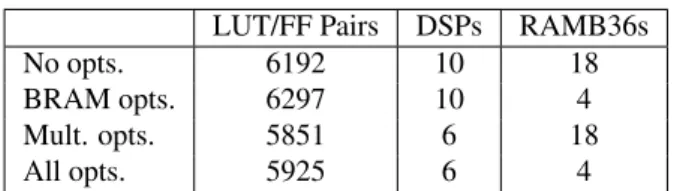
5.2. Implementation Results
For synthesis we target our filter design to a Xil-inx Virtex-5 LX110T FPGA, with a clock frequency of 250MHz. At this speed, with data arriving and exiting the circuit once per cycle, we achieve a sustained computation rate of 1GB/s.
Table 2 shows the area impact of the Photon optimiza-tion graph-passes on the filter hardware. The multiplier power of two substitution pass reduces the number of DSP blocks used from 10 to 6, and the delay merging pass re-duce BRAM usage from 18 RAMB36s to 4. The number of LUTs required for the original and optimized designs are similar.
LUT/FF Pairs DSPs RAMB36s
No opts. 6192 10 18
BRAM opts. 6297 10 4
Mult. opts. 5851 6 18
All opts. 5925 6 4
Table 2. Resource usage for 2D convolution filter on a Virtex 5 with various optimizations.
6. Conclusion
In this paper we introduce Photon, a Java-based FPGA programming tool. We describe the programming model for Photon in which data I/O is separated from computation allowing designs to implicitly be easy to pipeline and hence perform well in an FPGA. We give an overview of Photon’s implementation as a library directed by user created Java programs. Finally, we present a case study demonstrating that Photon’s pluggable optimization system can be used to improve the resource utilisation of designs. Our current and future work with Photon includes developing a system for making it easier to create the data I/O logic external to Photon designs, and creating more advanced optimization passes.
References
[1] J. A. Bower, W. N. Cho, and W. Luk, “Unifying FPGA hard-ware development,” in International Conference on Field-Programmable Technology, December 2007, pp. 113–120. [2] Impulse Accelerated Technologies Inc., “ImpulseC,”
http://www.impulsec.com/, 2008.
[3] Agility, “DK design suite,” http://www.agilityds.com/, 2008. [4] O. Mencer, M. Morf, and M. J. Flynn, “PAM-Blox: High
performance FPGA design for adaptive computing,” in IEEE Symposium on FPGAs for Custom Computing Machines, Los Alamitos, CA, 1998, pp. 167–174.
[5] P. Bellows and B. Hutchings, “JHDL - An HDL for reconfig-urable systems,” in IEEE Symposium on FPGAs for Custom Computing Machines, Los Alamitos, CA, 1998, pp. 175 – 184.
[6] O. Mencer, “ASC: A stream compiler for computing with FPGAs,” IEEE Transactions on CAD of ICs and Systems, vol. 25, pp. 1603–1617, 2006.
[7] P. Hudak, “Modular domain specific languages and tools,” Intl. Conf. on Software Reuse, vol. 00, p. 134, 1998. [8] O. Pell and R. G. Clapp, “Accelerating subsurface offset
gath-ers for 3D seismic applications using FPGAs,” SEG Tech. Program Expanded Abstracts, vol. 26, no. 1, pp. 2383–2387, 2007.
[9] D. B. Thomas, J. A. Bower, and W. Luk, “Hardware archi-tectures for Monte-Carlo based financial simulations,” in In-ternational Conference on Field-Programmable Technology, December 2006, pp. 377–380.
Automated Design Approach for On-Chip Multiprocessor Systems
P. Mahr, H. Ishebabi, B. Andres, C. Loerchner, M. Metzner and C. Bobda
Department of Computer Science, University of Potsdam, Germany
{pmahr,ishebabi,andres,lorchner,metzner,bobda}@cs.uni-potsdam.de
Abstract
This paper presents a design approach for adaptive mul-tiprocessor systems-on-chip on FPGAs. The goal in this particular design approach is to ease the implementation of an adaptive multiprocessor system by creating compo-nents, like processing nodes or memories, from a parallel program. Therefore message-passing, a paradigm for par-allel programming on multiprocessor systems, is used. The analysis and simulation of the parallel application provides data for the formulation of constraints of the multiprocessor system. These constraints are used to solve an optimization problem with Integer Linear Programming: the creation of a suitable abstract multiprocessor hardware architecture and the mapping of tasks onto processors. The abstract ar-chitecture is then mapped onto a concrete arar-chitecture of components, like a specific Power-PC or soft-core proces-sor, and is further processed using a vendor tool-chain for the generation of a configuration file for an FPGA.
1. Introduction
As apparent in current developments the reduction of transistor size and the exploitation of instruction-level par-allelization can not longer be continued to enhance the per-formance of processors [1]. Instead, multi-core processors are a common way of enhancing performance by exploiting parallelism of applications. However, designing and im-plementing multiple processors on a single chip leads to new problems, which are absent in the design of single-core processors. For example, an optimal communication infrastructure between the processors needs to be found. Also, software developers have to parallelize their applica-tions, so that the performance of the application is increased through multiple processors. In the case of multiproces-sor systems-on-chip (MPSoCs), which combine embedded heterogeneous or homogeneous processing nodes, memory systems, interconnection networks and peripheral compo-nents, even more problems arise. Partly because of the va-riety of technologies available and partly because of their sophisticated functionality [2] [3]. To reduce design time,
high level design approaches can be employed. In [4] ,[5], [6] and [7] design methodologies and corresponding tool-support are described.
In principle two communication paradigms for parallel computing with multiprocessor systems exist, the commu-nication through shared memory (SMP), i. e. cache or mem-ory on a bus-based system, and the passing of messages (MPI) through a communication network. SMP architec-tures, like the Sun Niagara processor [8] or the IBM Cell BE processor [9], are the common multiprocessors today. MPI is typically used in computer clusters, where physically dis-tributed processors communicate through a network.
This paper presents a survey about our developments in the area of adaptive MPSoC design with FPGAs (Field-Programmable Gate Arrays) as a flexible platform for Chip-Multi-Processors. In section 2 an overview of the proposed design approach for MPSoCs is given. Therefore the steps for architectural synthesis, starting with the analysis and simulation of a parallel program and ending with the gen-eration of a bitfile for the configuration of an FPGA are de-scribed in general. In the following section 3 an on-chip message passing software library for communication be-tween tasks of a parallel program, and a benchmark for the purpose of evaluation are presented. Section 4 summarizes the formulation of architecture constraints for the design space exploration with Integer Linear Programming. These constraints are formulated out of the results of the analysis and simulation of a parallel program. The following sec-tion 5 gives an overview about the creasec-tion of MPSoCs us-ing abstract components. Finally, this paper is concluded in section 6 and a brief overview about future work is given in section 7.
2. System design using architectural synthesis
To get an efficient multiprocessor system-on-chip from a parallel program several approaches are possible. In figure 1 our proposed synthesis flow using an analytical approach is shown. The architectural synthesis flow starts with paral-lel applications that are modeled as a directed graph, where
the nodes represent tasks and the edges represent communi-cation channels [10].
Figure 1. Architectural Synthesis Flow
In the first step of the design flow, information on data traffic and on task precedence is extracted from functional simulations of the parallel program. Information on the number of cycles of a task when executed on a specific pro-cessor is determined from cycle accurate simulations. This information is used to formulate an instance of an Integer Linear Programming (ILP) problem.
In the following step, called Abstract Component cre-ation, a combinatorial optimization is done by solving an ILP problem. Additionally to the information gathered in the first step, platform constraints, e. g. area and speed of the target platform, are needed as well. As a result of this step an abstract system description including the (abstract) hard- and software parts is generated.
The third step is called Component mapping. The ab-stract system description, which consists of abab-stract pro-cessors, memories, communication components or hard-ware accelerators and softhard-ware tasks linked onto abstract processors, is mapped on a concrete architecture of com-ponents like PPC405, MicroBlaze or on-chip BRAMs. If needed, an operating systems can be generated with scripts and makefiles and can be mapped onto a processor as well. This step can be done using the PinHaT software (Platform-independent Hardware generation Tool) [11].
In the final step a bitfile is generated from the concrete components using the platform vendor tool-chain perform-ing logic synthesis and place & route. However, simulations for the validation of the system on higher and lower levels
is needed as well and should be performed during the pro-posed steps.
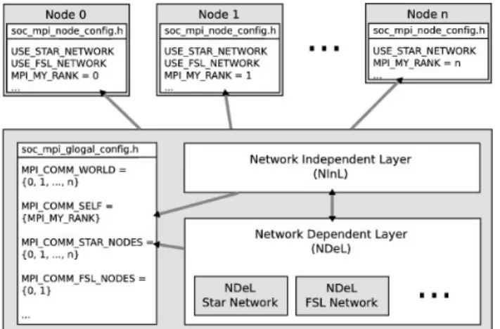
3. On-Chip Message Passing
In this section the on-chip communication between pro-cessing nodes using a subset of the MPI standard is scribed [12]. Therefore a small-sized MPI-library was de-veloped (see figure 2), which is similar to the approaches described in [13], [14] and [15].
Figure 2. SoC-MPI Library
The library consists of two layers. A Network indepen-dent layer (NInL) and a network depenindepen-dent layer (NDeL), for the separation of the hardware dependent part from the hardware independent part of the library. The advan-tage of this separation is the easy migration of the library to other platforms. The NInL provides MPI functions, like MPI Send, MPI Receive, MPI BSend or MPI BCast. These functions are used to perform the communication be-tween processes in the program. The NDeL is an accumu-lation of network dependent functions for different network topologies. In this layer the ranks and addresses for con-crete networks are determined and the cutting and send-ing of messages dependsend-ing on the chosen network is car-ried out. Currently the length of a message is limited to 64 Bytes, due to the limited on-chip memory of FPGAs. Longer messages are therefore cutted into several smaller messages and are send in series. The parameters of the MPI functions, like count, comm or dest (destination), are also used as signals and parameters for the hardware compo-nents of the network topology. That is, the parameters are used to build the header and the data packets for the commu-nication over a network. The MPI parameters are directly used for the control, data and address signals.
Init, Finalize, Initialized, Wtime, Wtick, Send, Recv, SSend, BSend, RSend, SendRecv, Barrier, Gather, BCast, Comm Size, Comm Rank.
Figure 3. Configuration of processing nodes
In figure 3 several processing nodes are connected to-gether via a star network. Additionally node 0 and 1 are directly connected together via FSL (Fast Simplex Link) [16]. Each processing node has only a subset of the SoC-MPI Library with the dependent functions for the network topology.
3.1. Benchmarks
The MPI library is evaluated using Intel MPI Bench-marks 3.1, which is the successor of the well known pack-age PMB (Pallas MPI Benchmarks) [17]. The MPI imple-mentation was benchmarked on a Xilinx ML-403 evaluation platform [18], which includes a Virtex 4 FPGA running at 100MHz. Three MicoBlaze soft-core processors [19] were connected together via a star network. All programs were stored in the on-chip memories.
In Figure 4 the results of the five micro benchmarks are shown. Due to the limited on-chip memory not all bench-marks could be performed completely. Furthermore, a small decay between 128 and 256 Bytes message size exists, be-cause the maximum MPI message length is currently lim-ited to 251 KBytes and a message larger than that must be splitted into several messages. Further increase of the mes-sage size would lead to a bandwidth closer to the maximum possible bandwidth, which is limited through the MicroB-laze and was measured with approximately 14 MBytes/s.
4. Abstract component creation using Integer
Linear Programing
In this flow, Integer Linear Programming (ILP) is used for automated design space exploration with the goal of
lo-Figure 4. Benchmarks of the SOC-MPI Library
cating the best possible abstract architecture for a given par-allel application under given constraints. The simultaneous optimization problem is to map parallel tasks to a set of pro-cessing elements and to generate a suitable communication architecture, which meets the constraints of the target plat-form, and minimizes the overall computation time of the parallel program. The input for this step is obtained by us-ing a profilus-ing tool for the mpich2 package. In the followus-ing two subsections area and time constraints of processors and communication infrastructure are described in separate.
4.1. Processors - sharing constraint, area constraint
and costs
A few assumptions about processors and tasks need to be made, because it is possible to map several tasks on a processor: (1) a task scheduler exists, so that scheduling is not involved in the optimization problem. (2) Task mapping is static. (3) The instruction sequence of a task is stored on the local program memory of the processor, e. g. instruction cache, and hence the size of the local program memory limits the number of tasks, which can be mapped onto a processor. (4) Finally the cost of switching tasks in terms of processor cycles does not vary from task to task. Let Ii ∈ I0, ..., In be a task, Jj ∈ J0, ..., Jm a processor and xij = 0, 1 a binary decision variable, whereas xij = 1 means that task Iiis mapped onto processor Jj.
m X
j=0
xij= 1, ∀Ii (1)
A constraint for task mapping (equation 2), called ad-dress space constraint, and the cost of task switching (equa-tion 3) can be formulated, where sijis the size of a task Ii of a processor Jj with the program memory size sj and tj is the cost (time) of task switching.
n X i=0 xij· sij≤ sj, ∀Ii (2) TSW IT CH= m X j=0 n X i=0 xij· tj (3)
For the calculation of the area of the processors AP E the area of of a single processor aj is needed. Because xij only shows if a task Ii is mapped onto a processor Jj and does not show the number of processors in the system or the number of instantiations of a processor, an auxiliary variable vj = 0, 1 is needed. For each instance of a pro-cessor Jj there is a corresponding virtual processor vj and for all tasks mapped to a certain processor there is only one task which is mapped to the corresponding virtual proces-sor. This leads to the following constraint (equation 4) so that the area of the processors can be calculated with equa-tion 5. vj≤ n X i=0 xij, ∀Jj (4) AP E≥ m X j=0 vij· aj (5)
4.2. Communication networks - Network capacity
and area constraint
Several assumptions have to be made before constraints about the communication network can be formulated. The communication of two tasks mapped onto the same proces-sor is done via intra-procesproces-sor communication, which have a negligible communication latency and overhead, com-pared to memory access latency. All processors can use any of the available communication networks and can use more then one network. A communication network has arbitra-tion costs resulting from simultaneous access on the net-work. It is assumed, that tasks are not prioritized and an up-per bound on arbitration time for each network can be com-puted for each network topology depending on the number of processors. Finally, it is not predictable when two or more tasks will attempt to access the network. Though a certain probability can be assumed.
λi1,i2is an auxiliary 0-1 decision variable that is 1, if two communicating tasks are mapped on different processors. The sum of xi1j1 and xi2j2 equals two if the tasks are on
different processors as seen in equation 6. λi1,i2=
xi1j1+ xi2j2
2 (6)
A communication topology Ck∈ C0, ..., Ckmay have a maximum capacity of processors attached to it. This con-straint is described in equation 7. yk is a binary decision
variable with value 1 if a communication topology Ck is used for communication between two tasks Ii1and Ii2, and 0 otherwise. Ii1 l Ii2 is a precedence operator. Ii1 is
pre-ceded by Ii2 which means, that a data transfer is performed
from Ii1to Ii2. The maximum number of processes, which
can use a topology Ckis described by Mk. yk+
X
Ii1,Ii2|Ii1lIi2
λi1,i2≤ Mk, ∀Ck (7)
The total area cost of the communication network (re-sources for routing) can be calculated with equation 8, where Akis the area cost of topology Ck.
AN ET ≥ m X
j=0
Ak· yk (8)
The cost of the topology in terms of computation time is calculated in 10, whereas zki1i2is a binary decision
vari-able, which is 1 if a network will be used by two tasks. Oth-erwise the variable zki1i2is 0. Di1i2is the amount of data to
be transferred between the two communicating tasks and pk is the probability that network arbitration will be involved when a task wants to communicate. The upper bound arbi-tration time is τk. zki1i2 ≥ λi1,i2+ yk− 1 (9) TN ET = X Ii1,Ii2|Ii1lIi2 K X k=0 (Di1i2+ τk· pk)zki1i2 ! (10)
Finally the total area cost A is calculated form the area of the processing elements AP E (equation 5) and the area for the routing resources AN ET (equation 8).
A ≥ AP E+ AN ET (11)
The cost of computation time can be calculated with equation 12, whereas Tijis the time requirement to process a task Iion a processor Jj. The objective, in this case, is to minimize computation time of a (terminating) parallel pro-gram. However for non-terminating programs, like signal processing programs, the objectives are different.
T = min m X j=0 n X i=0 xij· Tij+ TN ET+ TSW IT CH (12)
5. Component Mapping
In this section the mapping of abstract components onto concrete ones is described. This component-based approach is similar to the one described by Ces´ario et al. [20], where a high-level component-based methodology and design en-vironment for application-specific MPSoC architectures is presented. For this task, a component-based design environ-ment called PinHaT for the generation and configuration of the system infrastructure was developed. This environment offers a vendor independent framework with which users can specify the requirements of their system and automati-cally produce the necessary system configuration and start-up code. The Tool was developed as a Java application.
Generally PinHaT follows a two-step approach. In the first step an abstract specification of the system using ab-stract components like CPUs, Memories or Hardware Ac-celerators are described. In the following step these abstract components will be refined and mapped to concrete com-ponents, e. g. a specific CPU (PPC405, MicrocBlaze) or a Hardware-Divider. Also the software tasks are mapped onto the concrete components. The structure of PinHaT is shown in figure 5. A detailed overview about the PinHaT tool is given in [11].
Figure 5. Structure of PinHaT
The component mapping is divided into the generation and the configuration of the system infrastructure, where hardware is generated and software is configured. In this flow, the input to PinHaT is obtained by high level synthe-sis, as described in section 4.
5.1. Generation of the System Infrastructure
The generation of the system infrastructure, that is the mapping of an abstract system description onto a concrete hardware description, is done by PinHaT. PinHaT uses XML in conjunction with a document type definition file (DTD) as an input for the abstract system description. An input consists of valid modules, which are CPU, Memory, Communication Modules, Periphery and Hardware Accel-erator. The hardware mapping onto concrete components is divided into three phases.
In the first phases an internal XML tree is build by pars-ing the input file. For all nodes of this tree an adequate class is instantiated. These classes know how to process its own parameters. Such classes can be easily added to the framework to extend the IP-Core base. In a subsequent step, another parser creates the platform specific hardware information file from the gathered information. In the sec-ond phase individual mappers for all components and target platforms, are created, followed by the last phase, where a mapper creates the platform dependent hardware descrip-tion files. These dependent hardware descripdescrip-tion files are then passed to the vendor’s tool chain, e. g. Xilinx EDK or Altera Quartus II.
5.2. Configuration of the System Infrastructure
-SW Mapping
In the case of software, a task is mapped onto a concrete processor. This is in contrast to the mapping of abstract components, e. g. processors or memories, to concrete ones during the generation of the system infrastructure.
For the mapping step, parameters of the software must be specified for each processor. The parameters include in-formation about the application or the operating system, like source-code, libraries or the os-type. With these in-formation scripts and Makefiles for building the standalone applications and the operating systems are created. While standalone applications only need compiling and linking of the application, building the operating system is more dif-ficult. Depending of the operating system, different steps, like configuration of the file-system or the kernel parame-ters, are necessary. The result of the task mapping is an executable file for each processor in the system.
6. Conclusion
In this paper a concept for the design automation of mul-tiprocessor systems on FPGAs was presented. A small-sized MPI library was implemented to use message passing for the communication between tasks of a parallel program. Simulation and analysis of the parallel program is carried
out to gather information about task precedence, task in-teraction and data traffic between tasks. These informa-tion is needed to formulate constraints, for the solving of an Integer Linear Programming problem. As a result an abstract system description, consisting of hardware compo-nents, like processing nodes or hardware accelerators, and linked tasks is created. With the help of the PinHaT soft-ware the components of the abstract system description can be mapped onto concrete components, like specific proces-sors. Finally the configuration file for an FPGA can be cre-ated using the vendor tool-chain.
7. Future Work
Currently the PinHaT software is being extended into an easy to use software solution including the architectural synthesis of a parallel program. Also new abstract and cor-responding concrete components, like new network topolo-gies or processing nodes like the OpenRISC processor will be included to enhance flexibility of the architectural syn-thesis flow. Furthermore concepts of adaptivity of multipro-cessor systems are to be analysed and a detailed evaluation of on-chip message-passing in the face of communication overhead and latency needs to be carried out.
References
[1] Kunle Olukotun and Lance Hammond. The future of micro-processors. Queue, 3(7):26–29, 2005.
[2] Wayne Wolf. The future of multiprocessor systems-on-chips. In DAC ’04: Proceedings of the 41st annual conference on Design automation, pages 681–685, New York, NY, USA, 2004. ACM.
[3] Gilles Sassatelli, Nicolas Saint-Jean, Cristiane Woszezenki, Ismael Grehs, and Fernando Moraes. Architectural issues in homogeneous noc-based mpsoc. In RSP ’07: Proceedings of the 18th IEEE/IFIP International Workshop on Rapid System Prototyping, pages 139–142, Washington, DC, USA, 2007. IEEE Computer Society.
[4] D.D. Gajski, Jianwen Zhu, R. Dmer, A. Gerstlauer, and Shuqing Zhao. SpecC: Specification Language and Method-ology. Springer, 2000.
[5] Tero Kangas, Petri Kukkala, Heikki Orsila, Erno Salmi-nen, Marko H¨annik¨aiSalmi-nen, Timo D. H¨am¨al¨aiSalmi-nen, Jouni Ri-ihim¨aki, and Kimmo Kuusilinna. Uml-based multiprocessor soc design framework. Trans. on Embedded Computing Sys., 5(2):281–320, 2006.
[6] Simon Polstra. A systematic approach to exploring embed-ded system architectures at multiple abstraction levels. IEEE Trans. Comput., 55(2):99–112, 2006. Member-Andy D. Pi-mentel and Student Member-Cagkan Erbas.
[7] Blanca Alicia Correa, Juan Fernando Eusse, Danny Munera, Jose Edinson Aedo, and Juan Fernando Velez. High level
system-on-chip design using uml and systemc. In CERMA ’07: Proceedings of the Electronics, Robotics and Automo-tive Mechanics Conference (CERMA 2007), pages 740–745, Washington, DC, USA, 2007. IEEE Computer Society. [8] Poonacha Kongetira, Kathirgamar Aingaran, and Kunle
Olukotun. Niagara: A 32-way multithreaded sparc proces-sor. IEEE Micro, 25(2):21–29, 2005.
[9] J. A. Kahle, M. N. Day, H. P. Hofstee, C. R. Johns, T. R. Maeurer, and D. Shippy. Introduction to the cell multipro-cessor. IBM J. Res. Dev., 49(4/5):589–604, 2005.
[10] Concepcio Roig, Ana Ripoll, and Fernando Guirado. A new task graph model for mapping message passing applications. IEEE Trans. Parallel Distrib. Syst., 18(12):1740–1753, 2007. [11] Christophe Bobda, Thomas Haller, Felix M¨uhlbauer, Dennis Rech, and Simon Jung. Design of adaptive multiprocessor on chip systems. In SBCCI ’07: Proceedings of the 20th annual conference on Integrated circuits and systems design, pages 177–183, New York, NY, USA, 2007. ACM.
[12] MPI Forum. http://www.mpi-forum.org/. 01. April 2008.
[13] J. A. Williams, I. Syed, J. Wu, and N. W. Bergmann. A reconfigurable cluster-on-chip architecture with mpi com-munication layer. In FCCM ’06: Proceedings of the 14th Annual IEEE Symposium on Field-Programmable Custom Computing Machines, pages 350–352, Washington, DC, USA, 2006. IEEE Computer Society.
[14] T. P. McMahon and A. Skjellum. empi/empich: Embedding mpi. In MPIDC ’96: Proceedings of the Second MPI Devel-opers Conference, page 180, Washington, DC, USA, 1996. IEEE Computer Society.
[15] Manuel Salda˜na and Paul Chow. Tmd-mpi: An mpi imple-mentation for multiple processors across multiple fpgas. In FPL, pages 1–6, 2006.
[16] Xilinx Fast Simplex Link (FSL). http://www.xilinx. com/products/ipcenter/FSL.htm. 07. August 2008.
[17] Intel MPI Benchmarks. http://www.intel.com/ cd/software/products/asmo-na/eng/219848. htm. 09. April 2008.
[18] Xilinx ML403 Evaluation Platform. http: //www.xilinx.com/products/boards/ml403/ reference_designs.htm. 09. April 2008.
[19] Xilinx MicroBlaze Processor. http://www.xilinx. com/products/design_resources/proc_ central/microblaze.htm. 09. April 2008.
[20] W. Ces´ario, A. Baghdadi, L. Gauthier, D. Lyonnard, G. Nico-lescu, Y. Paviot, S. Yoo, A. A. Jerraya, and M. Diaz-Nava. Component-based design approach for multicore socs. In DAC ’02: Proceedings of the 39th conference on Design au-tomation, pages 789–794, New York, NY, USA, 2002. ACM.
ASM++ charts: an intuitive circuit representation
ranging from low level RTL to SoC design
S. de Pablo, L.C. Herrero, F. Martínez
University of Valladolid
Valladolid (Spain)
sanpab@eis.uva.es
M. Berrocal
eZono AG
Jena (Germany)
manuel@ezono.com
Abstract
This article presents a methodology to describe digital circuits from register transfer level to system level. When designing systems it encapsulates the functionality of several modules and also encapsulates the connections between those modules. To achieve these results, the possibilities of Algorithmic State Machines (ASM charts) have been extended to develop a compiler. Using this approach, a System-on-a-Chip (SoC) design becomes a set of linked boxes where several special boxes encapsulate the connections between modules. The compiler processes all required boxes and files, and then generates the corresponding HDL code, valid for simulation and synthesis. A small SoC example is shown.
1. Introduction
System-on-a-Chip (SoC) designs integrate processor cores, memories and custom logic joined into complete systems. The increased complexity requires more effort and more efficient tools, but also an accurate knowledge on how to connect new computational modules to new peripheral devices using even new communication protocols and standards.
A hierarchical approach may encapsulate on black boxes the functionality of several modules. This technique effectively reduces the number of components, but system integration becomes more and more difficult as new components are added every day.
Thus, the key to a short design time, enabling “product on demand”, is the use of a set of predesigned components which can be easily integrated through a set of also predesigned connections, in order to build a product.
Because of this reason, Xilinx and Altera have proposed their high end tools named Embedded Development Kit [1] and SoPC Builder [2], respectively, that allow the automatic generation of systems. Using these tools, designers may build complete SoC designs based on their processors and peripheral modules in few hours. At a lower scale, similar results may be found on the Hardware Highway (HwHw) web tool [3].
On the language side a parallel effort has been observed. In particular, SystemVerilog [4] now include an ‘interface’ element that allow designers to join several inputs and outputs together in one named description, so textual designs may become easier to read and understand. At a different scale, pursuing a higher level of abstraction, the promising SpecC top-down methodology [5] firstly describes computations and communications at an abstract and untimed level, and then descends to an accurate and precise level where connections and delays are fully described.
The aim of this paper is to contribute to these efforts from a bottom-up point of view, mostly adequate for academic purposes. First of all, we present several extensions to the Algorithmic State Machine (ASM) methodology, what we have called “ASM++ charts”, allowing the automatic generation of VHDL or Verilog code from this charts, using a recently developed ASM++ compiler. Furthermore, these diagrams may describe hierarchical designs and define, through special boxes, how to connect different modules all together.
2. ASM++ charts
The Algorithmic State Machine (ASM) method for specifying digital designs was originally documented on 1973 by C.R. Clare [6], who worked at the Electronics Research Laboratory of Hewlett Packard Labs, based on previous developments made by T. Osborne at the University of California at Berkeley [6]. Since then it has been widely applied to assist designers in expressing algorithms and to support their conversion into hardware [7-10]. Many texts on digital logic design cover the ASM method in conjunction with other methods for specifying Finite State Machines (FSM) [11-12].
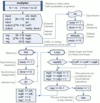
A FSM is a valid representation of the behavior of a digital circuit when the number of transitions and the complexity of operations is low. The example of fig. 1 shows a FSM for a 12x12 unsigned multiplier that computes ‘outP = inA * inB’ through twelve conditional additions. It is fired by a signal named ‘go’, it signals the answer using ‘done’, and indicates through ‘ready’ that new operands are welcome.
Figure 1. An example of FSM for a multiplier.
However, on these situations traditional ASM charts may be more accurate and consistent. As shown at fig. 2, they use three different boxes to fully describe the behavior of cycle driven RTL designs: a “state box” with rectangular shape defines the beginning of each clock cycle and may include unconditional operations that must be executed during (marked with ‘=’) or at the end (using the delay operator ‘←’) of that cycle; “decision boxes” –diamond ones– are used to test inputs or internal values to determine the execution flow; and finally “conditional output boxes” –with oval shape– indicate those operations that are executed during the same clock cycle, but only when previous conditions are valid. Additionally, an “ASM block” includes all operations and decisions that are or can be executed simultaneously during each clock cycle.
Figure 2. Traditional ASM chart for a multiplier.
The advantages of FSM for an overall description of a module are evident, but the ASM representation allows more complex designs through conditions that are introduced incrementally and detailed operations located where designer specifies.
However, ASM notation has several drawbacks:
– They use the same box, rectangular ones, for new
states and unconditional operations executed at those states. Because of this property, ASM diagrams are compact, but they are also more rigid and difficult to read.
– Sometimes it is difficult to differentiate the frontier
between different states. The complexity of some states requires the use of dashed boxes (named ASM blocks) or even different colors for different states.
– Due to the double meaning of rectangular boxes,
conditional operations must be represented using a different shape, the oval boxes. But, actually, all operations are conditional, because all of them are state dependent.
– Additionally, designers must use lateral annotations
for state names, for reset signals or even for links between different parts of a design (see fig. 2).
– Finally, the width of signals and ports cannot be
specified when using the current notation.
Proposed ASM++ notation [13-14] tries to solve all these problems and extend far beyond the possibilities of this methodology. The first and main change introduced by this new notation, as seen at fig. 3, is the use of a specific box for states –we propose oval boxes, very similar to those circles used in bubble diagrams– thus now all operations may share the same box, a rectangle for synchronous assignments and a rectangle with bent sides for asynchronous assertions. Diamonds are kept for decision boxes because they are commonly recognized and accepted.
Figure 3. ASM++ chart ready for compilation.
Figure 3 shows additional features of ASM++ charts, included to allow their automatic compilation to generate HDL code. In addition to an algorithmic part, a declarative section may describe the design name, its implementation parameters, the external interface, one or more internal signals. The synchronization signal and its reset sequence can be fully specified in a very intuitive way too. A box for ‘defaults’ has been added to easily describe the circuit behavior when any state leave any signal free. Furthermore, all boxes use standard VHDL or Verilog expressions, but never both of them; the ASM++ compiler usually detects the HDL and then generates valid HDL code using the same language.
3. Hierarchical design using ASM++ charts
As soon as a compiler generates the VHDL or Verilog code related to an ASM++ chart, the advanced features of modern HDL languages can be easily integrated on them. The requirements for hierarchical design have been included through the following elements:– Each design begins with a ‘header’ box that
specifies the design name and, optionally, its parameters or generics.
– Any design may use one or several pages on a MS
Visio 2007 document1, saved using its VDX format.
Each VDX document may include several designs identified through their header boxes.
– Any design may instantiate other designs, giving
them an instance name. As soon as a lower level module is instantiated, a full set of signals named “instance_name.port_name” (see fig. 5) is created to ease the connections with other elements. Later on, any ‘dot’ will be replaced by an ‘underline’ because of HDL compatibility issues.
– When the description of an instantiated module is
located on another file, a ‘RequireFile’ box must be used before the header box to allow a joint compilation. However, the ASM++ compiler identifies any previously compiled design to avoid useless efforts and invalid duplications.
– VHDL users may include libraries or packages
using their ‘library’ and ‘use’ sentences, but also before any header box.
– Nowadays, compiler does not support reading
external HDL files, in order to instantiate hand written modules. A prototype of them, as shown at fig. 4, can be used instead.
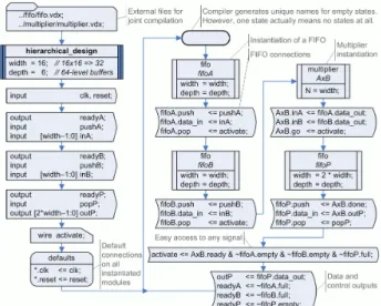
Using these features, an example with a slightly improved multiplier can be easily designed. First of all, a prototype of a small FIFO memory is declared, as shown at fig. 4, thus compiler may know how to instantiate and connect this module, described elsewhere on a Verilog file. Then three FIFO memories are instantiated to handle the input and output data flows, as shown at fig. 5, so several processors may feed and retrieve data from this processing element.
Figure 4. A prototype of an external design.
1 Actually, designers may also use MS Visio 2003 or ConceptDraw.
However, the only supported file format is VDX.
Figure 5. An example of hierarchical design.
The ASM++ chart of fig. 5 can be compared with its arranged compilation result, shown below. The advantages of this methodology on flexibility, clarity and time saving are evident. Not always a text based tool is faster and more productive than a graphical tool.
module hierarchical_design (clk, reset, inA, inB, outP, readyA, readyB, readyP, pushA, pushB, popP); parameter width = 16; // 16x16 => 32
parameter depth = 6; // 64-level buffers
input clk, reset; output readyA; input pushA; input [width-1:0] inA; output readyB; input pushB; input [width-1:0] inB; output readyP; input popP; output [2*width-1:0] outP; wire activate;
wire fifoA_clk, fifoA_reset; wire [width-1:0] fifoA_dataIn, fifoA_dataOut; wire fifoA_push, fifoA_pop; wire fifoA_empty, fifoA_full; fifo # (
.width(width), .depth (depth) ) fifoA (
.clk (fifoA_clk), .reset (fifoA_reset), .data_in (fifoA_dataIn), .data_out (fifoA_dataOut), .push (fifoA_push), .pop (fifoA_pop), .empty (fifoA_empty), .full (fifoA_full) );
wire fifoB_clk, fifoB_reset; wire [width-1:0] fifoB_dataIn, fifoB_dataOut; wire fifoB_push, fifoB_pop; wire fifoB_empty, fifoB_full; fifo # (
.width(width), .depth (depth) ) fifoB (
.clk (fifoB_clk), .reset (fifoB_reset), .data_in (fifoB_dataIn), .data_out (fifoB_dataOut), .push (fifoB_push), .pop (fifoB_pop), .empty (fifoB_empty), .full (fifoB_full) );


![Figure 6 describes a small SoC that implements a Harvard-like DSP processor (see [13]) connected to a program memory, a 32-level FIFO and a register](https://thumb-eu.123doks.com/thumbv2/5dokorg/5455948.141543/23.892.470.802.291.853/figure-describes-implements-harvard-processor-connected-program-register.webp)

