Halmstad University Post-Print
Reconfigurable Optical
Interconnection System
Supporting Concurrent
Application-Specific Parallel Computing
Sacki Agelis and Magnus Jonsson
N.B.: When citing this work, cite the original article.
©2005 IEEE. Personal use of this material is permitted. However, permission to reprint/republish this material for advertising or promotional purposes or for creating new collective works for resale or redistribution to servers or lists, or to reuse any copyrighted component of this work in other works must be obtained from the IEEE.
Agelis S, Jonsson M. Reconfigurable optical interconnection system supporting concurrent application-specific parallel computing. In: 17th Symposium on Computer Architecture and High Performance Computing: SBAC-PAD 2005 : proceedings : 24-27 October, 2005, Rio de Janeiro, PR, Brazil. IEEE; 2005. p. 44-51.
DOI: http://dx.doi.org/10.1109/CAHPC.2005.35
Copyright: IEEE
Post-Print available at: Halmstad University DiVA
Reconfigurable Optical Interconnection System
Supporting Concurrent Application-Specific Parallel Computing
Sacki Agelis and Magnus Jonsson
CERES – CENTRE FOR RESEARCH ON EMBEDDED SYSTEMS
School of Information Science, Computer and Electrical Engineering, Halmstad University, Box 823, S-301 18, Halmstad, Sweden. Sacki.Agelis@ide.hh.se, http://www2.hh.se/staff/saag
Abstract
Application specific architectures are highly desirable in embedded parallel computing systems at the same time as designers strive for using one embedded parallel computing platform for several applications. If this can be achieved the cost can be decreased in comparison to using several different embedded parallel computing systems. This paper presents a novel approach of running several high-performance applications concurrently on one single parallel computing system. By using a reconfigurable backplane interconnection system the applications can be run efficiently with high network flexibility since the interconnect network can be adapted to fit the application that is being processed for the moment. More precisely, this paper investigates how the Space Time Adaptive Processing (STAP) radar algorithm and the stripmap Synthetic Aperture Radar (SAR) algorithm can be mapped on a multi-cluster processing system with a reconfigurable optical interconnection system realized by a Micro-Optical-Electrical Mechanical System (MOEMS) crossbars. The paper describes the reconfigurable platform, the two algorithms and how they individually can be mapped on the targeted multiprocessor system. It is also described how these two applications can be mapped simultaneously on the optical reconfigurable platform. Implications and requirements on communication bandwidth and processor performance in different critical points of the two applications are presented. The results of the analysis show that an implementation is feasible with today’s MOEMS technology, and that the two applications can be successfully run in a time-sharing scheme, both at the processing side and at the access for interconnection bandwidth.
1 Introduction
Today’s embedded computer systems are typically multi-board-based platforms with printed circuit boards (PCB) interconnected through a backplane network. Each PCB typically holds a few processors and some memory banks and the entire system often needs to be small (area-efficient), have low power consumption, be easy to upgrade, have long lifetime (often decades), etc. The backplane typically has harsh environmental constraints on it that allows it to work properly for many years. As the PCBs and their components are upgraded to handle more
data and more computations they set new demands on the backplane interconnection system.
Optics and optical communication technology has been around for quite some time now and yet they are not really adopted into the world of embedded systems, even though they are widely used in the rest of the data communication society. Some research groups have made similar investigations, e.g., the Gemini project [1]. The Gemini project presented several solutions for optical backplanes with electro-optical architectures [1] and introduced an inter-PCB switch fabric composed of active optical switch elements of refractive type. Our paper shows how and why new optical communication systems can be used for application specific purposes in embedded parallel computing. The paper describes an optical technology that is mature enough to be considered for next generation reconfigurable application specific embedded systems. In our previous work we have investigated how optical network architectures can be incorporated into parallel communication systems such as routers and switches [2], where we have showed that the power of reconfigurability in communication equipment is best applied in the backplane where the highest gain is achieved to the lowest cost [2].
Moreover, today’s embedded supercomputers are typically designed to handle one specific application in an efficient way in order to achieve as high computational performance as possible. This is a rather inflexible way of using embedded parallel computers and it is highly desirable to have the vast advantage, economically as well as functionally, to be able to run several applications on one single embedded computer and still be able to make the embedded computer perform at its very best with the given components that are used. In turn this gives the system the ability to be a multi-application specific machine, but not being a general purpose machine. This ability is achieved by adding a few optical components to deploy reconfigurability in the backplane communication system. Additionally, the components and the technologies described in this paper can be used today and the prices for these technologies are expected to fall quite significantly the next few years. They are also expected to have a significant impact on the communication arena through out the world.
The paper encompasses a case study of using a high performance multi-processor architecture with a reconfigurable application specific interconnection architecture for two very different kinds of high-performance demanding applications. These applications
typically demand their own separate embedded multiprocessor system, but by using system-level reconfigurability in the interconnection architecture both applications can be run simultaneously on a single processor system. This is partly achieved by using Micro-Optical-Electrical Mechanical System (MOEMS) crossbars to deploy the reconfigurability in the optical interconnection system. This reconfigurability gives each application a multi-stage shuffle interconnection network that is suited for the behavior of the algorithm itself. In the field of reconfigurable computing and reconfigurable networking MOEMS devices are relatively unproven, especially for embedded parallel computing. Primarily because up until now MOEMS devices where considered too unstable, too expensive etc. Reports and articles are now emerging that claims MOEMS former flaws can be thought of as its strengths [3].
The applications are two radar algorithms with two different purposes. They are both used in airborne and ground based radar sites with various setups, depending on what the user is mostly interested in. The first application, Space-Time Adaptive Processing (STAP), is a moving target indication algorithm. The second application is the stripmap Synthetic Aperture Radar (SAR), which is used to create topological maps of the surrounding geographical terrain.
The fundamental base of using reconfigurability is to be able to use one processing platform for several applications as efficiently as possible. There are different types of reconfigurability. There is processor reconfigurability and communication (interconnection network) reconfigurability, and here we will focus on the latter, namely system level reconfigurability for the application specific network properties of the backbone. In comparison to the reconfigurable interconnection network, a static over-dimensioned interconnection network can be used instead. This, inherently, means that since the static network is non-reconfigurable it has to be considerably over-dimensioned which it typically is so that communication bottlenecks can be coped with. By having reconfigurability in the communication network higher network performance is achieved.
The two radar algorithms have somewhat different demands. The STAP is widely known for its computational saturation while the SAR is memory intense in comparison to the STAP. As these different typical demands are known we decide to use, roughly, the per-processor load of 70% for the STAP leaving at most 30% per-processor load for the SAR. This constraint has to be met at the individual mapping of each algorithm, roughly estimated. However, note that the final mapping that includes both algorithms, obviously, must not exceed 100% per-processor load. The backbone data bandwidth demands will be investigated and the same time-sharing cycle as for the processing time is assumed to apply at the backbone shuffle network, i.e. 70% of the network time is allocated for STAP and the remaining 30% for SAR. Concerning the reconfigurable platform a total number of 144 processing elements (PEs) are used distributed over
eight modules, where each module holds eighteen processing elements.
The reconfigurable platform is described in Section 2 and the two algorithms and their respective bandwidth and processing demands are briefly described in Section 3 and Section 4. Each of the algorithms is individually mapped on the reconfigurable system in Section 5, followed by the mapping of both algorithms simultaneously. Finally, the paper is concluded in Section 6.
2 The reconfigurable platform
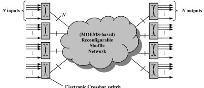
The reconfigurable platform is composed of multiple rack-mounted processing modules interconnected through a reconfigurable interconnection network as depicted in Figure 1. Each module is actually a PCB that holds 18 PEs, an input electronic packet-switch and an output
electronic packet-switch. We assume that each PE can
sustain 3.5 GFLOPS in performance. Hence, if 144 processor elements are used, the total sustained processing rate is 504 GFLOPS. All communications lead to/from the backplane where they are interconnected through a reconfigurable optical MOEMS crossbar switch, see Figure 2. This gives the opportunity to reconfigure the backbone network for different application characteristics and by doing so substantial performance speed up can be attained.
(MOEMS-based) Reconfigurable
Shuffle Network
Electronic Crossbar switch
N inputs N outputs
N
Figure 1: An overview of the interconnection system.
Vertical cavity surface emitting lasers (VCSELs) [4]
are used in the reconfigurable platform to transmit data from the first switch stage (the input stage), via the backplane interconnection network, to the second switch stage (the output stage). Today’s VCSEL components typically come in three different bit rate versions; 10 Gbit/s, 2.5 Gbit/s or 1.25 Gbit/s and VCSELs have had a rather dramatic impact on the optical communication domain the last five years and they are widely considered as the way of the future. VCSELs are low cost components at the same time as they offer low threshold current, easy fabrication through their monolithic construction, etc. They exist in, e.g., 850 nm, 1330 nm or 1550 nm wavelength components. Throughout the rest of this report we will assume 2.5 Gbit/s VCSELs with 20% communication overhead (control traffic, redundancy, logging information, etc) which results in 2 Gbit/s (250 MByte/s) in pure data capacity on one single link in the network.
Processor Element
Switch Reconfigurable Optical interconnection network
Figure 2: The logical layout for the reconfigurable parallel computer architecture.
As seen in Figure 2 the processors are logically connected to switch boards. Each processor transmits data to an input electronic packet-switch that holds N I/Os. In turn, the input switch transmits data over the backbone shuffle interconnection network to an output-queued electronic packet-switch. The output switches transmit data to the receiving side of the processor cluster. All switches are output-buffered packet-switches and are assumed to have, internally on each switch, enough short-distance data rate to match the backbone network. The switching latency, including traffic classification, destination address lookup and switch-fabric setup-time, is a fixed value and can be adapted by adding a constant in the delay analysis. We assume an output-buffered switch here, but an equivalent input-buffered switch architecture such as
Virtual Output Queuing is also feasible.
The number of I/Os on each switch must exceed the total number of switches in the input/output stage of the backbone shuffle network, i.e. N >M where M is the number of switches in each stage of the interconnect system. Throughout this report we will assume that N=18 and M=8. Hence, we have 144 PEs in total. Given this, we have 144× (250 MByte/s per VCSEL link) which is a total of 36 GByte/s in pure data capacity over the shuffle network.
Further, each input switch will have one dedicated communication line to each of the output switches in order to be able to offer instant bandwidth if so would be needed. Hence, the total number of data link I/Os in the network will be as many as processing nodes in the system, here 144. Moreover, this leads to N – M reconfigurable links per switch board, i.e. 10/18 = 55.56% of the total network resources are reconfigurable. Hence, out of the 36 GByte/s in backbone network resources, 20 GByte/s are reconfigurable to the disposal of the programmer. The reason for having one communication link between each input/output switch-pair is that additional data such as logging information, control traffic, data overhead, etc, should be able to be transferred throughout the system at any time, without waiting for the reconfigurable interconnection backbone to configure itself (to set up a connection).
The ability to reconfigure the backbone network is supplied by using Micro-Optical-Electrical Mechanical Systems (MOEMS). These optical components are
MOEMS with 8 u 8, 16 u 16 or 32 u 32 pop-mirrors, as illustrated in Figure 3.
The actuated flip-flop mirrors are monolithically integrated on a silicon chip. By pushing a selected mirror, the collimated light is redirected to the desired output port as shown in Figure 3. The micro-actuated flip-flop switch mirror consists of a mirror (usually gold or aluminum) that provides a reflective surface to the incoming light beam. For so called 2D MOEMS the optical beams move in a two-dimensional space where each mirror is controlled to be in either down-position (no beam bounce) or up-position (beam bounce). This technology is seen to achieve low light-loss, low crosstalk, and low polarization dependence as further described in [5]. One disadvantage with this technology is the relatively long reconfiguration time, which is in the order of milliseconds. The MOEMS should, however, only be used to reconfigure the network topology, they should not be regarded as packet switches. To avoid that the MOEMS becomes a bottleneck in the sense that backbone shuffle network traffic might have to wait for a few milliseconds for an uplink to be configured there will always be one uplink available from each input switch to each output switch as mentioned above.
Because these devices steer light beams they are bit rate independent, wavelength (i.e. channel) independent as well as protocol independent. This means that, theoretically, 80 or more wavelengths are possible at 10 Gbit/s per fiber, i.e. 800 Gbit/s in total per fiber [6]. Significantly important is that each device in a MOEMS system is relatively large so this technology does not push the limits of lithography and wafer fabrication processes. In general, last generation semiconductor processing equipment can be used.
Figure 3: An NuN optical switch with pop-up mirrors,
i.e. N2 MOEMS mirrors.
Reports show that 112 u 112 switches with the capacity of 35.8 Tbit/s are possible and reliable [7]. Lucent Technologies has announced 238 u 238 switches based on the 3-dimensional MOEMS technology with 56 644 possible connections, while switch sizes of 1024 u 1024 are prototyped and 4096 u 4096 port MEMS are considered to be reality in the next few following years. Finally, due to the relatively low signal attenuation of 2 dB in today’s MOEMS devices, multistage MOEMS switches are also possible. This low attenuation is significantly important since it reduces the power requirements of the optical transmitters and receivers; hence the cost is also reduced.
3 Space Time Adaptive Processing
Space-Time Adaptive Processing (STAP) is a very
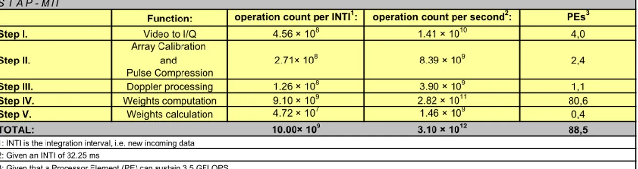
computational intensive radar application, with high resolution. It is used for moving target indication (MTI) radars. The STAP MTI-radar that we will focus on here is a case study that originates in [8], and consists of five specific computational stages, as depicted in Table 1. The first stage is a data conversion step which is called Video
to I/Q. After this, array calibration and pulse compression
is performed in the second step followed by the Doppler processing in the third stage.
Further, weight computations are performed in the two last stages of this algorithm. Given that the integration interval (INTI) of 32.25 ms is given the following number of operations are required, see Table 1. Two estimations are given, one for the number of operations required for one single INTI, and one for the number of operations per second that is required in order to sustain the STAP continuously. The sustained performance adds up to over 300 GFLOPS for the given INTI interval, which means that over 88 processors will be needed (100% per-PE load) in order to be able to sustain such a performance, see Table 1.
The data distribution within the STAP consists of 2×32 bit of data (complex numbers), i.e. 32 bits for the real part and 32 bits for the imaginary part. The size of the incoming data cube is number of channels L times the number of range bins N times the number of pulses P per INTI (L ×N ×P). Assuming 32 bit data resolution, the stated case give us a data cube matrix of total size 64×3840×64×32, i.e. 5.03×108 bits per INTI. This gives us 6.29×107 bytes which is 63 MByte per INTI. In order to
sustain the INTI interval of 32.25 ms the throughput must be 63 MByte/32.25 ms, i.e. 1951 MByte/s.
4 Stripmap Synthetic Aperture Radar
The stripmap Synthetic Aperture Radar (SAR) is used to produce topological maps in 3D, primarily for airborne and ground based avionic radar systems. SAR is known as a memory demanding algorithm as opposed to the STAP algorithm. The SAR algorithm exists in many various form and here we will focus on the stripmap SAR used to create topological ground maps in flying aircrafts. The basic idea is to use one antenna to create a synthetic aperture by taking multiple samples of several ground spots as the aircraft is moving in its flight direction. Data is recorded over a wide time span of about 25-50 seconds (frame time). If 50% framing overlap is used, the frame time is reduced by half. All topological maps are saved and reused when the same area is revisited.
As opposed to the STAP, the SAR algorithm is more homogenously intensive in terms of required operations per step in the SAR chain. That is, the steps in the chain are fairly alike as for computational demands and memory demands. More information about SAR is given in [9].
The processing demands are specified in Table 2, where the minimum number of required processing elements in each step is given as depicted in the right-most column. This gives us a total number of operations over 5474 GFLOP. However, we have a rather long integration time (frame time) of 50 sec, so the required sustained operations per second ends up just above 109 GFLOPS. Note that Block 4, the pulse compression, is a substantial part of the total computational demands. Actually it constitutes over 46% of the total operations.
SAR
Source Sum Name GFLOP Data In (Mbyte/s) Data Out (Mbyte/s) GFLOPS Min #PEs Block 1 Complexity 3,33E+10 Format Conversion 33,3 1 333 2 666 0,67 0,19
Block 2 and 3 Complexity 3,67E+11 Azimuth Filter 366,6 2 666 1 333 7,33 2,10
Block 4 Complexity 2,54E+12 Pulse Compression 2 542,6 1 333 333 50,85 14,53
Block 5 Complexity 2,87E+11 Motion Compensation 1 287,5 333 333 5,75 1,64
Block 6 Complexity 2,87E+11 Motion Compensation 2 287,5 333 333 5,75 1,64
Block 7 Complexity 3,61E+11 Azimuth FFT 361,3 667 667 7,23 2,06
Block 8 Complexity 3,04E+11 Range FFT 304,3 667 667 6,09 1,74
Block 9 Complexity 6E+11 Stolt Interpolation 599,9 667 667 12,00 3,43
Block 10 Complexity 2,5E+10 Matched Filter 25,0 667 667 0,50 0,14
Block 11 Complexity 3,04E+11 Range IFFT 304,3 667 667 6,09 1,74
Block 12 Complexity 3,61E+11 Azimuth IFFT 361,3 667 667 7,23 2,06
Total: 5 473,8 109,5 31,28
Table 2: Bandwidth and performance requirements for SAR, assuming a frame time of 50 seconds.
S T A P - MTI
Function: operation count per INTI1: operation count per second2: PEs3
Step I. Video to I/Q 4.56 × 10⁸ 1.41 × 10¹⁰ 4,0
Array Calibration
Step II. and 2.71× 10⁸ 8.39 × 10⁹ 2,4
Pulse Compression
Step III. Doppler processing 1.26 × 10⁸ 3.90 × 10⁹ 1,1
Step IV. Weights computation 9.10 × 10⁹ 2.82 × 10¹¹ 80,6
Step V. Weights calculation 4.72 × 10⁷ 1.46 × 10⁹
0,4
TOTAL: 10.00× 10⁹ 3.10 × 10¹² 88,5
1: INTI is the integration interval, i.e. new incoming data 2: Given an INTI of 32.25 ms
3: Given that a Processor Element (PE) can sustain 3.5 GFLOPS
5 Individual mappings of the STAP and SAR
Next, we will investigate how to map the two algorithms individually on the reconfigurable platform. In particular, there are three demands that have to be examined; processing power in each algorithm function step, data bandwidth to/from each processing node, and data bandwidth in the backbone interconnection network.
5.1 STAP on the reconfigurable platform
It is imperative to see how many processors are used in each step for the data throughput that is required. In Table 3 it is showed how many PEs are required at minimum in each function step in the STAP given a link capacity of 250 MByte/s with 70% network access time. Observe that the maximum amount of PEs has to be chosen from the two columns in the middle in Table 3, so that the bandwidth requirements are met at the processor side of the system. At least 58 PEs have to be used to meet the requirement of the communication rate.
In Table 4 both bandwidth considerations and processing power considerations are regarded for the STAP map on the reconfigurable platform. The map for STAP is sufficient in all aspects that are needed in order to handle the amount of incoming data. It can also be seen that the per-processor load is within the 70% rule and that, in fact, the last six processors are underutilized even though there is a need for all of them, for the sake of data
bandwidth management. Also, note that the first three steps in STAP are merged to be run on the same processors. This way of combining several function steps, as above in Table 4, is a trade off of reducing backbone traffic and increasing local memory demands at the processing nodes. This gives us the final map of the STAP on the reconfigurable platform in the rightmost column of Table 4.
The mapping of the processors and the data bandwidth can now be set and an implementation layout on the reconfigurable platform has been carried out as seen in Table 5. It can be seen that 128 Mbytes are transferred over the backbone network for each integration interval for the STAP algorithm. This adds up to near 4 GByte/s of continuous backbone bandwidth, and in order to achieve this 22.67 backbone links are required to be used in the backbone shuffle network. This concludes the individual STAP mapping on the reconfigurable platform.
5.2 SAR on the reconfigurable platform
Let’s determine the layout of the SAR application over the processors and see what the required input switch to output switch demand is, i.e. how to configure the network resources to fit the application characteristics. There are a number of ways to map SAR on the reconfigurable platform, see Table 6. Let’s see how much per-processor performance is actually required for the different SAR maps. A direct minimal map (that originates from Table 2) of the performance requirements can be seen
STAP Network Requirements
Processing Block Input switch To output switch From PE To PE MByte/frame MByte/s Links required Step 1, Step 2 and Step 3 1 1 1 to 16 17 to 18 (2/122) × 96 = 1,57 48,8 0,28 Step 1, Step 2 and Step 3 1 2 1 to 16 19 to 36 (18/122) × 96 = 14,2 439,1 2,51 Step 1, Step 2 and Step 3 1 3 1 to 16 37 to 54 (18/122) × 96 = 14,2 439,1 2,51 Step 1, Step 2 and Step 3 1 4 1 to 16 55 to 72 (18/122) × 96 = 14,2 439,1 2,51 Step 1, Step 2 and Step 3 1 5 1 to 16 73 to 90 (18/122) × 96 = 14,2 439,1 2,51 Step 1, Step 2 and Step 3 1 6 1 to 16 91 to 108 (18/122) × 96 = 14,2 439,1 2,51 Step 1, Step 2 and Step 3 1 7 1 to 16 109 to 126 (18/122) × 96 = 14,2 439,1 2,51 Step 1, Step 2 and Step 3 1 8 1 to 16 127 to 138 (12/122) × 96 = 9,44 292,7 1,67
Step 4 1 8 17 to 18 139 to 141 (2/122) × 32 = 0,52 16,3 0,09 Step 4 2 8 19 to 36 139 to 141 (18/122) × 32 = 4,72 146,4 0,84 Step 4 3 8 37 to 54 139 to 141 (18/122) × 32 = 4,72 146,4 0,84 Step 4 4 8 55 to 72 139 to 141 (18/122) × 32 = 4,72 146,4 0,84 Step 4 5 8 73 to 77 139 to 141 (5/122) × 32 = 1,31 40,7 0,23 Step 4 5 8 78 to 90 142 to 144 (13/122) × 32 = 3,41 105,7 0,60 Step 4 6 8 91 to 108 142 to 144 (18/122) × 32 = 4,72 146,4 0,84 Step 4 7 8 109 to 126 142 to 144 (18/122) × 32 = 4,72 146,4 0,84 Step 4 8 8 127 to 138 142 to 144 (12/122) × 32 = 3,15 97,6 0,56 6 127,97 3967,9 22,67
Table 5: The final STAP mapping on the reconfigurable platform.
Minimum required amount of PEs for data bandwidth
Function Data bandwidth in Data bandwidth out Total requirement
Video to I/Q 12 6 12
Array calibration and pulse comp. 6 6 6
Doppler processing 6 17 17
Weight computation 17 6 17
Weight calculation 6 6 6
6 47 41 58
Table 3: Minimum amount of processing elements that is required to achieve enough bandwidth in each step of the STAP algorithm, given 70% access of the network time and 250 MByte/s per link capacity.
STAP - Mapping processor demands and data capacity demands
Function Data bandwidth Map STAP min PE-map Intermidiate map per-PE load intermidiate map Final Map per-PE load final map
Video to I/Q 12 4,04 12 0,337
Array calibration and pulse comp. 6 2,37 6 0,395
Doppler processing 17 1,11 17 0,066 16 0,472
Weight computation 17 80,60 81 1,000 122 0,661
Weight calculation 6 0,42 6 0,070 6 0,070
6 58 88,54 122 144
Weighted Average 0,615
Table 4: The final STAP map on the reconfigurable platform, given that a maximum of 70% per-PE load. The table shows how many processor elements need to be used for the final mapping of STAP.
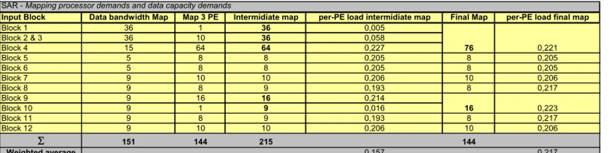
in column Map 1, Table 6. However, this map does not exploit all the available processors. However, the per-processor load should be lowered below 30%. This leads us to the intermediate step Map 2, and finally, Map 3 where all 144 PEs are used for SAR and as seen in Table 7 all individual processors have a per-processor load of less than 30%.
Input Block Min #Pes Map 1 Map 2 Map 3
Block 1 0,19 1 1 1 Block 2 & 3 2,10 3 6 10 Block 4 14,53 15 30 64 Block 5 1,64 2 4 8 Block 6 1,64 2 4 8 Block 7 2,06 3 6 10 Block 8 1,74 2 2 8 Block 9 3,43 4 8 16 Block 10 0,14 1 2 1 Block 11 1,74 2 4 8 Block 12 2,06 3 6 10 6 31,28 38 73 144
Table 6: Different maps of the SAR. SAR - Map 3
Input Block Min #Pes Map 3 per-PE load
Block 1 0,19 1 0,19 Block 2 & 3 2,10 10 0,21 Block 4 14,53 64 0,23 Block 5 1,64 8 0,21 Block 6 1,64 8 0,21 Block 7 2,06 10 0,21 Block 8 1,74 8 0,22 Block 9 3,43 16 0,21 Block 10 0,14 1 0,14 Block 11 1,74 8 0,22 Block 12 2,06 10 0,21 6 31,28 144 Weighted Average 0,22
Table 7: Weighted average per-PE load for Map 3. The maximum per-processor load for Map 3 is 23% (Block 4), which gives us a maximum performance demand of 0.23×3.5 GFLOPS, i.e. 0.805 GFLOPS. This is less than the 1.05 GFLOPS (30% of 3.5 GFLOPS) that was allocated for SAR and, hence, acceptable. This is the
first mapping structure for SAR on the reconfigurable platform. The switch-to-switch requirements for this mapping are according to Table 8. It can be seen that, in total, over 400 GByte of data needs to be distributed for one single SAR frame.
Assuming a frame time of 50 seconds, the continuous switch-to-switch requirement is about twice the STAP demand (about 4 GByte/s), adding up to a total of 8.3 GByte/s for SAR. This gives a total requirement of 111.23 backbone shuffle network links. It is important to note that the most bandwidth is required between input switch number one and output switch number one (row 1 with 35.47 links and row 2 with 1.95 links, see Table 8).
As explained previously, the requirements for how many processor nodes are needed in order grasp the tremendous amount of data in each function step of the SAR needs to be determined. This is clarified in Table 9 were the minimum amount of processing elements is determined according to their ability to process incoming and transmit outgoing data at the maximum rate of 250 MByte/s and with an network access of 30%. When Table 9 is combined with the minimum amount of processing power that is needed in each function step some interesting features emerge. In Table 10 both data bandwidth on the processor side as well as processing power is considered in order to create a new map for SAR In the intermediate map, Table 10, 166 PEs are needed even though there is only access to 144 PEs. The solution for this problem is to combine several function steps, here,
Block 1 to Block 4 and Block 9 to Block 10. This increases
the per-processor load for these processors. However, that is tolerable since the per-processor load is quite low for these functions in the intermediate map. In total, this gives the final mapping for SAR on the reconfigurable platform where a maximum per-PE load of 22.3% is noted (Block 9 and Block 10).
SAR switch-to-switch requirements
Processing Block From PCB To PCB From PE To PE GB/s (GB/frame) Amount of links
Block 1 1 1 1 2 to 11 2,660 133,0 35,47 Block 2 & 3 1 1 2 to 11 12 to 18 0,147 7,3 1,95 Block 2 & 3 1 2 2 to 11 19 to 36 0,377 18,8 5,02 Block 2 & 3 1 3 2 to 11 37 to 54 0,377 18,8 5,02 Block 2 & 3 1 4 2 to 11 55 to 72 0,377 18,8 5,02 Block 2 & 3 1 5 2 to 11 73 to 75 0,063 3,1 0,84 Block 4 1 5 12 to 18 76 to 83 0,036 1,8 0,49 Block 4 2 5 19 to 36 76 to 83 0,094 4,7 1,25 Block 4 3 5 37 to 54 76 to 83 0,094 4,7 1,25 Block 4 4 5 55 to 72 76 to 83 0,094 4,7 1,25 Block 4 5 5 73 to 75 76 to 83 0,016 0,8 0,21 Block 5 5 5 76 to 83 84 to 90 0,292 14,6 3,90 Block 5 5 6 76 to 83 91 0,042 2,1 0,56 Block 6 5 6 84 to 90 92 to 101 0,301 15,0 4,01 Block 6 6 6 91 92 to 101 0,033 1,7 0,45 Block 7 6 6 92 to 101 102 to 108 0,585 29,2 7,79 Block 7 6 7 92 to 101 109 0,084 4,2 1,11 Block 8 6 7 102 to 108 110 to 125 0,601 30,1 8,02 Block 8 7 7 109 110 to 125 0,067 3,3 0,89 Block 9 7 7 110 to 125 126 0,668 33,4 8,91 Block 10 7 8 126 127 to 134 0,668 33,4 8,91 Block 11 8 8 127 to 134 135 to 144 0,668 33,4 8,91 6 8,342 417,1 111,23
Minimum required PE for data bandwidth
Minimum number Minimum number
Input Block of PEs for data of PEs for data PEs required bandwidth in bandwidth in Block 1 18 36 36 Block 2 & 3 36 18 36 Block 4 18 5 15 Block 5 5 5 5 Block 6 5 5 5 Block 7 9 9 9 Block 8 9 9 9 Block 9 9 9 9 Block 10 9 9 9 Block 11 9 9 9 Block 11 9 9 9 136 123 151
Table 9: Minimum amount of processing elements that is required to achieve enough bandwidth in each step of the STAP algorithm.
Finally, a feasible implementation mapping of SAR is found. This mapping has the backbone network requirements as depicted in Table 11, where over 183 GByte has to be transferred over the backbone network for each integration interval, and 3.67 GByte/s in sustained rate. The most network traffic is located at the lower half of the reconfigurable backbone shuffle network. In terms of required networks links, see the rightmost column in Table 11, there is a total demand of almost 49 network links.
5.3 Simultaneous map of the STAP and SAR
Conceptually, the idea here is to be able to use the same multiprocessor platform for several algorithms if the platform is given the ability of having a reconfigurable system network, here, realized by the MOEMS to provide application-specific shuffle interconnection network. It is verified that either one of the algorithms occupy to much backbone network resources or processing power because
of the limitations that were set in the introduction. The STAP is only allowed to use, at maximum, 70% of the processing power on each processor and 70% network time. For the final STAP map we saw that the per-processor load is at most 66.1% (see Table 4). Inherently, this means that the SAR can occupy, at maximum, 33.9% per-processor load. For the final SAR map we saw that the maximum per-PE load is 22.3%. This leaves us with a worst case margin per-processor load slack of 100% í 66.1% í 22.3% = 11.6%. Therefore, it can be concluded that the processor performance is enough to run the STAP and the SAR simultaneously in a time-shared mode, and that the overall processor utilization is high, but not too high.
Finally, in the backplane shuffle network STAP requires 22.67 links and SAR requires 48.98 links, see Table 12. This gives the total link demand of 28 links for STAP and 55 links for SAR. Out of the 28 STAP links, 13 links need to be reconfigurable. Remember that each input switch has one static link to each of the outgoing switches to ensure instant bandwidth between any pair. This constraint is set because the MOEMS takes a few milliseconds to reconfigure, and to avoid this waiting time to set up a link each input switch has a default connection to each output switch. For SAR, 44 links need to be reconfigurable out of the 55 backplane shuffle network links. This means that each application will have its own time share of computing and backbone communication.
This approach will require twin buffers everywhere, i.e. one dedicated buffer queue for STAP and one dedicated buffer queue for SAR application so that when the network is reconfigured for the other application it will start using its respective buffers accordingly. For the time shared simultaneous mapping of SAR and STAP the network will switch between these two network modes at SAR - Mapping processor demands and data capacity demands
Input Block Data bandwidth Map Map 3 PE Intermidiate map per-PE load intermidiate map Final Map per-PE load final map
Block 1 36 1 36 0,005 Block 2 & 3 36 10 36 0,058 Block 4 15 64 64 0,227 76 0,221 Block 5 5 8 8 0,205 8 0,205 Block 6 5 8 8 0,205 8 0,205 Block 7 9 10 10 0,206 10 0,206 Block 8 9 8 9 0,193 8 0,217 Block 9 9 16 16 0,214 Block 10 9 1 9 0,016 16 0,223 Block 11 9 8 9 0,193 8 0,217 Block 12 9 10 10 0,206 10 0,206 6 151 144 215 144 Weighted average 0,157 0,217
Table 10: The final SAR map on the reconfigurable platform, given that a maximum of 30% per-PE load.
SAR Network Requirements
Processing Block Input switch To output switch From PE To PE GByte/frame GByte/s links required Block 1, Block 2, Block 3 and Block 4 1 5 1 to 18 77 to 84 (18/76) × 16,7 = 3,96 0,079 1,055 Block 1, Block 2, Block 3 and Block 4 2 5 19 to 36 77 to 84 (18/76) × 16,7 = 3,96 0,079 1,055 Block 1, Block 2, Block 3 and Block 4 3 5 37 to 54 77 to 84 (18/76) × 16,7 = 3,96 0,079 1,055 Block 1, Block 2, Block 3 and Block 4 4 5 55 to 72 77 to 84 (18/76) × 16,7 = 3,96 0,079 1,055 Block 1, Block 2, Block 3 and Block 4 5 5 73 to 76 77 to 84 (4/76) × 16,7 = 0,88 0,018 0,234
Block 5 5 5 77 to 84 85 to 90 (6/8) × 16,7 = 12,53 0,251 3,340 Block 5 5 6 77 to 84 91 to 92 (2/8) × 16,7 = 4,18 0,084 1,113 Block 6 5 6 85 to 90 93 to 102 (6/8) × 16,7 = 12,53 0,251 3,340 Block 6 6 6 91 to 92 93 to 102 (2/8) × 16,7 = 4,18 0,084 1,113 Block 7 6 6 93 to 102 103 to 108 (6/8) × 33,4 = 25,05 0,501 6,680 Block 7 6 7 93 to 102 109 to 110 (2/8) × 33,4 = 8,35 0,167 2,227 Block 8 6 7 103 to 108 111 to 126 (6/8) × 33,4 = 25,05 0,501 6,680 Block 8 7 7 109 to 110 111 to 126 (2/8) × 33,4 = 8,35 0,167 2,227
Block 9 and Block 10 7 8 111 to 126 127 to 134 33,4 0,668 8,907
Block 11 8 8 127 to 134 135 to 144 33,4 0,668 8,907
6 183,7 3,674 48,987
the same time as the PEs will time-share their processing between STAP and SAR. The two network modes will require switching between the STAP mode that requires 13 reconfigurable links, and the SAR mode that requires 44 reconfigurable links. This is feasible with the described optical and reconfigurable interconnection network.
6 Conclusions
In this paper it has been showed that the STAP algorithm and the stripmap SAR can be mapped on an embedded multiprocessor platform with reconfigurable application-specific interconnection network in the backplane. Further, the reconfigurable platform has been described with its reconfigurable interconnection system empowered by MOEMS devices.
It has been showed how each algorithm can be individually mapped on the reconfigurable platform, as well as bandwidth and processing requirements. However, issues such as application skew and buffer allocation issues (buffer synchronization etc) were not treated since the two applications are run in a time-shared scheme for processor and network usage.
In conclusion, the resources in the backbone are sufficient for STAP and SAR to be run in a time shared access scheme. However, this is an implementation study with two diverging algorithms, where each algorithm can be tuned by adding or subtracting features to them. Inherently, this increases or decreases the demands on processing power, data bandwidth in the backbone etc. In this way the application requirements versus the system performance can be load-balanced. However, the point of this case study is not to determine an ideal solution, but to prove the feasibility and conceptuality of using a multiprocessor system with reconfigurable interconnection network to run several embedded applications simultaneously and to provide application-specific advantages to increase total system performance.
7 References
[1] R. D. Chamberlain, G. D. Peterson, M. A. Franklin, and M. A. Province, “Genetic epidemiology, parallel
algorithms, and workstation networks,” Proc. of the 28th
Hawaii International Conference on System Sciences,
vol. 5, 3-6 Jan. 1995, pp. 101-111.
[2] S. Agelis and M. Jonsson, “System-level runtime reconfigurability – optical interconnection networks for switching applications,” to appear in Proc. Engineering of
Reconfigurable Systems and Algorithms, Las Vegas, NV,
USA, 2004, pp. 155-162.
[3] Magnus Jonsson, “Optical interconnection technology in switches, routers and optical cross connects,” SPIE
Optical Networks Magazine, vol. 4, no. 4, 2003, pp. 20-34.
[4] F. Mederer, I. Ecker, R. Michalzik, G. Steinle, H. Riechert, B. Lunitz, J. Moisel, and D. Wiedenmann, “VCSEL transmitters for 10-Gigabit Ethernet: 1.3 µm wavelength VCSELs for metropolitan area networks and TO-packaged 850 nm wavelength VCSELs for data transmission over multimode fibers and optical backplane waveguides,” Proc. 52nd Electronic Components and
Technology Conference, 2002, pp. 5-11.
[5] L. Y. Lin, E. L. Goldstein, and R. W. Tkach, “Free-space micromachined optical switches for optical networking,” IEEE Journal on Selected Topics in
Quantum Electronics, vol. 5, no. 1, 1999, pp. 4-9.
[6] P. B. Chu, S. Lee and S. Park, “MEMS: the path to large optical crossconnects,” IEEE Communications
Magazine, vol. 40, no. 3, 2002, pp. 80-87.
[7] D. T. Nielson et al, “Fully provisioned 112 × 112 micro-mechanical optical crossconnect with 35.8 Tb/s demonstrated capacity,” Optical Fiber Communication
Conference, vol. 4, 2000, pp. 202-204.
[8] Kenneth C. Cain, Jose A. Torres and Ronald T. Williams, “RT_STAP: Real-Time Space-Time Adaptive Processing Benchmark,” Center for Air Force C3 Systems,
the MITRE Corporation, Bedford, Massachusetts, USA,
1997.
[9] Mikael Taveniku, “Stripmap SAR – application, block level diagrams and implementations issues”, technical
report, Mercury Computer Systems, Ma, USA, 2003. STAP and SAR Requirements
Input switch Output switch STAP Roundup STAP, total links Roundup STAP, total reconf. links SAR Roundup SAR, total links Roundup SAR, total reconf. links
1 1 0,28 1 0 0,00 0 0 1 2 2,51 3 2 0,00 0 0 1 3 2,51 3 2 0,00 0 0 1 4 2,51 3 2 0,00 0 0 1 5 2,51 3 2 1,05 2 1 1 6 2,51 3 2 0,00 0 0 1 7 2,51 3 2 0,00 0 0 1 8 1,76 2 1 0,00 0 0 2 5 0,00 0 0 1,05 2 1 2 8 0,84 1 0 0,00 0 0 3 5 0,00 0 0 1,05 2 1 3 8 0,84 1 0 0,00 0 0 4 5 0,00 0 0 1,05 2 1 4 8 0,84 1 0 0,00 0 0 5 5 0,00 0 0 3,58 4 3 5 6 0,00 0 0 4,45 5 4 5 8 0,84 1 0 0,00 0 0 6 6 0,00 0 0 7,79 8 7 6 7 0,00 0 0 8,91 9 8 6 8 0,84 1 0 0,00 0 0 7 7 0,00 0 0 2,23 3 2 7 8 0,84 1 0 8,91 9 8 8 8 0,56 1 0 8,91 9 8 6 22,67 28 13 48,98 55 44