Loop impedance measurement tool
75
0
0
Full text
(2) LiU-ITN-TEK-A--20/048-SE. Loop impedance measurement tool The thesis work carried out in Elektroteknik at Tekniska högskolan at Linköpings universitet. Johan Abrahamsson Norrköping 2020-08-28. Department of Science and Technology Linköping University SE-601 74 Norrköping , Sw eden. Institutionen för teknik och naturvetenskap Linköpings universitet 601 74 Norrköping.
(3) Abstract This master’s thesis presents a prototype of a hand-held measurement tool used to measure the loop impedance of ground loops using two current probes. This tool allows the user to find bad shield connections in a system without disconnecting the shielded cables. The thesis explains the theory behind the measurement method, hardware requirements and design, how the software works and a demonstration of the implemented graphical user interface. The tool is powered by a two-cell lithium-ion battery and has an integrated battery charger with cell balancing..
(4) Acknowledgments I would like to thank Linköpings University for the education that made this master’s thesis possible. At the university I would like to give and extra thank to my examiner Qin ZhongYe and my supervisor Amir Baranzahi for the advice and support I have gotten throughout the project. I am grateful to Saab Dynamics AB for allowing me this opportunity and the embrace received by all their employees. Special thanks to Clas Tegenfeldt, my supervisor at Saab Dynamics, whom came with much good information and explanations about the subject of this master’s thesis project. I would also like to thank my boss at Saab Dynamics, Mattias Karlsson, for being very supportive during the whole project and for the help with all the administrative problems.. iv.
(5) Contents Abstract. iii. Acknowledgments. iv. Contents. v. List of Figures. vii. List of Tables. ix. List of Acronyms. viii. 1. Introduction 1.1 Background . . . . . . . . . . . . . . . . . . . . . . . . . . . . . . . . . . . . . . . 1.2 Aim . . . . . . . . . . . . . . . . . . . . . . . . . . . . . . . . . . . . . . . . . . . . 1.3 Research questions . . . . . . . . . . . . . . . . . . . . . . . . . . . . . . . . . . .. 2. Shield Impedance Measurement Techniques and Implementation Requirements 2.1 Shielding Effectiveness . . . . . . . . . . . . . . . . . . . . . . . . . . . . . . . . 2.2 Transfer Impedance . . . . . . . . . . . . . . . . . . . . . . . . . . . . . . . . . . 2.3 Loop Resistance . . . . . . . . . . . . . . . . . . . . . . . . . . . . . . . . . . . . 2.4 Current Probe Injection . . . . . . . . . . . . . . . . . . . . . . . . . . . . . . . . 2.5 Filter . . . . . . . . . . . . . . . . . . . . . . . . . . . . . . . . . . . . . . . . . . 2.6 Battery management system . . . . . . . . . . . . . . . . . . . . . . . . . . . . . 2.7 DC-block . . . . . . . . . . . . . . . . . . . . . . . . . . . . . . . . . . . . . . . . 2.8 Analog switch . . . . . . . . . . . . . . . . . . . . . . . . . . . . . . . . . . . . . 2.9 DAC and DMA . . . . . . . . . . . . . . . . . . . . . . . . . . . . . . . . . . . . 2.10 Memory . . . . . . . . . . . . . . . . . . . . . . . . . . . . . . . . . . . . . . . . 2.11 ADC . . . . . . . . . . . . . . . . . . . . . . . . . . . . . . . . . . . . . . . . . .. . . . . . . . . . . .. 3 3 3 4 5 6 7 8 9 9 10 10. Design of Loop Impedance Measurement Tool 3.1 Measure Impedance . . . . . . . . . . . . . 3.2 Current probe fail detection . . . . . . . . . 3.3 Voltage probe . . . . . . . . . . . . . . . . . 3.4 Design alternatives . . . . . . . . . . . . . . 3.5 Components . . . . . . . . . . . . . . . . . . 3.6 Hardware design . . . . . . . . . . . . . . . 3.7 Software . . . . . . . . . . . . . . . . . . . . 3.8 System design . . . . . . . . . . . . . . . . . 3.9 Prototype . . . . . . . . . . . . . . . . . . . .. . . . . . . . . .. 11 11 16 16 17 24 26 34 39 41. Measurement Results 4.1 Laboratory work . . . . . . . . . . . . . . . . . . . . . . . . . . . . . . . . . . . .. 43 43. 3. 4. v. . . . . . . . . .. . . . . . . . . .. . . . . . . . . .. . . . . . . . . .. . . . . . . . . .. . . . . . . . . .. . . . . . . . . .. . . . . . . . . .. . . . . . . . . .. . . . . . . . . .. . . . . . . . . .. . . . . . . . . .. . . . . . . . . .. . . . . . . . . .. . . . . . . . . .. . . . . . . . . .. . . . . . . . . .. . . . . . . . . .. . . . . . . . . .. . . . . . . . . .. 1 1 2 2.
(6) 4.2 5. 6. Hardware evaluation . . . . . . . . . . . . . . . . . . . . . . . . . . . . . . . . . .. Discussion 5.1 Laboratory work . . . . . . 5.2 Power switch . . . . . . . . 5.3 PCB test pads . . . . . . . . 5.4 Power amplifier . . . . . . . 5.5 Filter design . . . . . . . . . 5.6 Battery management system 5.7 STM32 evaluation board . .. . . . . . . .. . . . . . . .. . . . . . . .. . . . . . . .. . . . . . . .. . . . . . . .. Conclusion. . . . . . . .. . . . . . . .. . . . . . . .. . . . . . . .. . . . . . . .. . . . . . . .. . . . . . . .. . . . . . . .. . . . . . . .. . . . . . . .. . . . . . . .. . . . . . . .. . . . . . . .. . . . . . . .. . . . . . . .. . . . . . . .. . . . . . . .. . . . . . . .. . . . . . . .. . . . . . . .. . . . . . . .. . . . . . . .. . . . . . . .. . . . . . . .. 47 50 50 50 50 51 51 51 51 52. Bibliography. 53. Appendices. 54. A Circuit Diagram. 55. B Assembly Drawing. 62. C Drawing. 64. vi.
(7) List of Figures 2.1 2.2 2.3 2.4 2.5 3.1 3.2 3.3 3.4 3.5 3.6 3.7 3.8 3.9 3.10. Two shielded boxes connected to the same ground plane, connected with a shielded cable and connectors. . . . . . . . . . . . . . . . . . . . . . . . . . . . . . . Ideal current probe . . . . . . . . . . . . . . . . . . . . . . . . . . . . . . . . . . . . . Filters: 1) RC low-pass filter and 2) Switched capacitor equivalent low-pass filter . DC-block capacitor equivalent RC-filter . . . . . . . . . . . . . . . . . . . . . . . . . LTSpice simulation of RC-filter in Figure 2.4 . . . . . . . . . . . . . . . . . . . . . . .. 3.19 3.20 3.21 3.22 3.23 3.24 3.25 3.26 3.27. Measurement setup . . . . . . . . . . . . . . . . . . . . . . . . . . . . . . . . . . . . . Loops with measured resistance . . . . . . . . . . . . . . . . . . . . . . . . . . . . . . Laboratory setup . . . . . . . . . . . . . . . . . . . . . . . . . . . . . . . . . . . . . . Voltage probe setup . . . . . . . . . . . . . . . . . . . . . . . . . . . . . . . . . . . . . STM32G474CE . . . . . . . . . . . . . . . . . . . . . . . . . . . . . . . . . . . . . . . . Zynq-7000 SoC . . . . . . . . . . . . . . . . . . . . . . . . . . . . . . . . . . . . . . . STM32H747I-DISCO Discovery kit . . . . . . . . . . . . . . . . . . . . . . . . . . . . STM32H747XI . . . . . . . . . . . . . . . . . . . . . . . . . . . . . . . . . . . . . . . . Schematic of the docking connectors for the STM32H747-DISCO . . . . . . . . . . . Table 10 from the STM32H747-DISCO User Manual displaying the functionality on each pin on the docking connector [STM32H747-DISCO-User-Manual] . . . . Schematic of the Battery management system . . . . . . . . . . . . . . . . . . . . . . Schematic of power amplifier . . . . . . . . . . . . . . . . . . . . . . . . . . . . . . . Schematic of one of the two identical filter circuits . . . . . . . . . . . . . . . . . . . LTSpice simulation of filter with signal input frequency 1kHz and filter clock set to 10kHz . . . . . . . . . . . . . . . . . . . . . . . . . . . . . . . . . . . . . . . . . . . LTSpice simulation of filter with signal input frequency 50kHz and filter clock set to 500kHz . . . . . . . . . . . . . . . . . . . . . . . . . . . . . . . . . . . . . . . . . . Schematic of external connectors, except the STM32H747-DISCO docking headers, and voltage references . . . . . . . . . . . . . . . . . . . . . . . . . . . . . . . . . . . Overview of the designed circuit board. . . . . . . . . . . . . . . . . . . . . . . . . . Overview of the different views on in the GUI and how the user can navigate between them . . . . . . . . . . . . . . . . . . . . . . . . . . . . . . . . . . . . . . . . Graphical design of the main view . . . . . . . . . . . . . . . . . . . . . . . . . . . . Graphical design of the settings view . . . . . . . . . . . . . . . . . . . . . . . . . . . Graphical design of the calibration view . . . . . . . . . . . . . . . . . . . . . . . . . Graphical design of the second calibration view . . . . . . . . . . . . . . . . . . . . Graphical design of the numpad view . . . . . . . . . . . . . . . . . . . . . . . . . . System diagram . . . . . . . . . . . . . . . . . . . . . . . . . . . . . . . . . . . . . . . Assembled PCB . . . . . . . . . . . . . . . . . . . . . . . . . . . . . . . . . . . . . . . Final prototype . . . . . . . . . . . . . . . . . . . . . . . . . . . . . . . . . . . . . . . Final prototype equipped with current probes . . . . . . . . . . . . . . . . . . . . .. 4.1 4.2 4.3. Four measurements with z = 100mΩ, VTx = 10kHz sine with various amplitudes . Measurement with z = 45mΩ, VTx = 10kHz sine wave . . . . . . . . . . . . . . . . . Measurement with z = 520mΩ, VTx = 10kHz sine wave . . . . . . . . . . . . . . . .. 3.11 3.12 3.13 3.14 3.15 3.16 3.17 3.18. vii. 4 5 6 8 9 11 15 15 16 18 19 21 22 26 27 28 29 30 31 31 32 33 35 36 36 37 37 38 40 41 41 42 43 44 44.
(8) Plot of calculated Areal from measurement data . . . . . . . . . . . . . . . . . . . . . Calculation example of the calibration constants using measurement data . . . . . Calculation example with measurement data from a loop with resistance = 45mΩ . Power Amplifier measurement with fixed input Vin = 2.5 + 0.05 ˚ sin(2π10000) V Power Amplifier measurement in time domain with two current probes and a 100mΩ ground loop . . . . . . . . . . . . . . . . . . . . . . . . . . . . . . . . . . . . 4.9 Power Amplifier measurement in frequency domain with two current probes and a 100mΩ ground loop . . . . . . . . . . . . . . . . . . . . . . . . . . . . . . . . . . . 4.10 Input filter measurement with 10kHz noisy sine wave as input . . . . . . . . . . . . 4.4 4.5 4.6 4.7 4.8. viii. 45 46 46 47 48 48 49.
(9) List of Tables 4.1. A calculations from data in Figure 4.1 . . . . . . . . . . . . . . . . . . . . . . . . . .. ix. 44.
(10) List of Acronyms AC Alternating Current ADC Analog to Digital Converter BMS Battery Management System DAC Digital to Analog Converter DC Direct Current DMA Direct Memmory Access DUT Device Under Test EMC Electromagnetic Compatibility FPGA Field-Programmable Gate Array I2C Inter-Integrated Circuit IDE Integrated Development Environment MCU Microcontroller Unit MOSFET Metal Oxide Semiconductor Field Effect Transistor PCB Printed Circuit Board PWM Pulse Width Modulation SE Shielding Effectiveness SoC System on a Chip SPI Serial Peripheral Interface SSR Solid-State Relay USB Universal Serial Bus Zt Transfer Impedance. viii.
(11) 1. Introduction. This master’s thesis designs and develops a measurement tool to measure shield impedance of cables within a system. This project was done as a master’s thesis at the Electronic Design Engineering program at Linköpings University provided by Saab Dynamics in Linköping, Sweden.. 1.1. Background. Saab Dynamics develops state-of-the-art electronics in safety-critical applications. This electronics need to work in the most extreme environments of cold, heat, vibration, interference and radiation. It should work flawlessly from the first second - even after 25 years. Everywhere, electronics are used which are becoming more advanced, compact, energy efficient and work with ever higher frequencies. We use more and more wireless technology for good and evil. Society’s growing dependence on electrical systems and communication systems today demands more and more that no one else interferes or is disturbed, that is what we call EMC. EMC stands for electromagnetic compatibility. The electromagnetic spectrum is a limited common resource. Therefore, different systems must be designed to work without interfering with each other. There are legal, commercial, technical, military, practical and theoretical aspects within EMC. Important parts of EMC are design, measurement technology, testing and verification. The electric fields, magnetic fields or radio frequency radiation that a product is in, is something we call the electrical environment. A mobile phone sends a radiation utility signal to communicate with the base station, but can at the same time interfere with radios and other electronics. In principle everything can be seen as a disturbance of the electrical environment. Disturbances can go wireless as an electromagnetic wave in space or follow wires, and an apparatus can interfere or be disturbed. In short, we have transmitter-channel-receivers and the EMC work tries to handle all three parts. A classic way is to try to shield themselves from the environment through dense metal boxes and use shielded cables between them. But what will happen if the cable is not connected properly? How can one detect a leak of interference caused by a cable and its connectors in existing systems currently in use?. 1.
(12) 1.2. Aim. 1.2. Aim. The aim of this master’s thesis work is to develop a practical method to measure how good a shielded cable is, where the connected equipment is in a complex system, even though the cable connector has been unscrewed and remounted many times. The method should then be realized by designing a portable measurement tool that easily can be used to measure the condition of a shielded cable without disconnecting it.. 1.3. Research questions. The main questions of this project are presented here and will be answered later in this report. 1. How can the loop impedance reveal the condition of a shielded cable? 2. How can a specific connector be examined to see if it has been oxidized without removing the connector? 3. How can a filter be designed to allow programmable center frequency?. 2.
(13) 2. 2.1. Shield Impedance Measurement Techniques and Implementation Requirements. Shielding Effectiveness. Shielding effectiveness is a dimensionless number, which describes how good a shield isolates the leakage of radiated emissions.[3] For any shielding barrier, shielding effectiveness (SE) is given by: [ E ( or H ) without shield] SE(dB) = 20log (2.1) [ E (or H ) with shield] By exposing a test cable of a strong known electromagnetic field, the shielding effectiveness can be calculated by measuring the electromagnetic field inside the cable between the shield and the core. In practice, this electromagnetic field is very hard to measure since it is confined between the shield and the core and hard to access with a measurement tool. Instead the voltage between shield and core can be measured while illuminating a strong electromagnetic field, but this method requires expensive measurement equipment and gives much room for measurement errors.[4]. 2.2. Transfer Impedance. Another way of measuring the condition of the shield is by measuring the transfer impedance (Zt ) for the cable shield. In contrast to measure the shielding effectiveness, this is a purely conducted measurement method with accurate results. But Zt has the dimension Ω/m and cannot be directly seen as the shield performance. It can however be used to calculate the shield performance [8]. The problem with this method is that it requires disassembly of the system to measure allow measurement of the transfer impedance of a specific shielded cable [11].. 3.
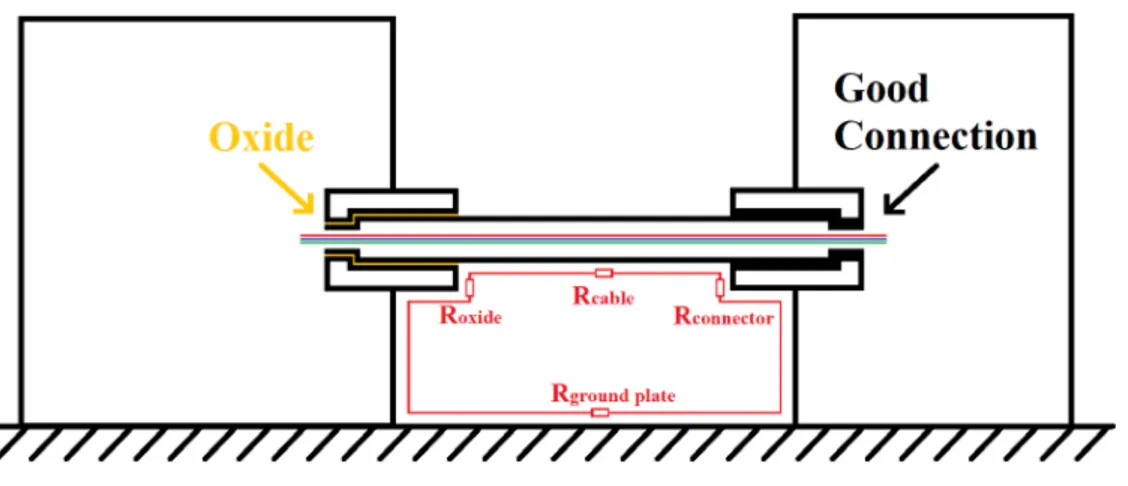
(14) 2.3. Loop Resistance. 2.3. Loop Resistance. By measuring a total resistance of a loop, a bad connector or a break can be found. Since a bad connector gives a higher resistance, there will be a relatively large potential over the connector. This potential can be measured to find where the bad connection is. This voltage measurement is required to determine if the total loop resistance is high because of a specific connector or if the conductivity in the whole loop is low.[6]. Figure 2.1: Two shielded boxes connected to the same ground plane, connected with a shielded cable and connectors. The loop resistance can be measured using two probes. One injecting probe which injects a strong signal with a low frequency. The signal is then measured using a measurement probe. If the losses at the specific frequency is known for the two probes, the loop resistance can be calculated. This is explained in detail in section 3.1 Measure Impedance. This method is good enough since the total max impedance of the shield is specified for most military products, and it gives a good first result to know if the shield performance need to be evaluated more in detail with more accurate methods.. 4.
(15) 2.4. Current Probe Injection. 2.4. Current Probe Injection. A current probe woks similar to a transformer with only one winding on one of the two sides. Figure 2.2 show an ideal current probe. When a current I flows through the conductor, magnetic flux B is generated in the core. This magnetic flux induces a current in the second wire which is proportional to the current I.[1] The magnetic flow in a coil with N turns can be explained with the formula NΦ = BA where Φ is the magnetic flow through one turn, B is the magnetic flux and A is the cross section area of the coil.. Figure 2.2: Ideal current probe [2] There are two types of current probes, injection probes and current monitor probes. These two probe types are very similar but have some differences. Current Injection Probe • Designed to inject power into cable. • Frequency range varies between different probe models. Normally, the frequency range is kHz to hundreds of MHz. • Maximum power that the probes can be fed with is usually between 75W and 200W. Current Monitor Probe • Designed to measure the amount of current flowing through a cable. • Frequency range varies between different probe models. Normally, the frequency range is kHz to hundreds of MHz. • Maximum current that the probe can measure is usually a few hundreds of amperes. Basically, the two probes are very similar. The current injection probe is usually bigger and designed to apply higher power. But both probe types are designed according to Figure 2.2 with a winded core. 5.
(16) 2.5. Filter. 2.5. Filter. Since the ground shield can be full of disturbances from other systems, a filter is needed to be able to only look at the signal that has been transmitted from the injection probe. There are several ways to do this. • Digital filter: Digital filtering is pretty simple since we know the frequency of the transmitted signal. The problem with only use digital filtering is that the disturbances can be much bigger than the signal that is to be measured. If that is the case, the ADC can be saturated which means that the sampled signal will be chopped and is hard to process. • Analog passive filter: An analog passive filter works well, but need to be designed for a certain center frequency and amplification since the passive filter attenuate the signal. Since two frequencies should be supported (1kHz and 40kHz) is is hard to do a filter that cover both frequencies without allowing the low frequency disturbances to pass. Two separate filters can be used to cover both the frequencies and a switch to choose which filter that is to be used. • Switched capacitor filter: A switched capacitor filter works like an analog passive filter, but instead of using resistors to set the filter properties, switched capacitors are used. A switched capacitor is a capacitor where MOSFET switches are used to control the flow of charge into and out from the capacitor. By using non-overlapping clocks to control the switches respective, the capacitor can be switched to behave like a resistor. This solution is available as integrated circuits where a clock frequency can be changed to change the center frequency of the filter.[5] Figure 2.3 shows a simple RC Low-pass filter and an equivalent Low-pass filter made using switched capacitors.. Figure 2.3: Filters: 1) RC low-pass filter and 2) Switched capacitor equivalent low-pass filter. 6.
(17) 2.6. Battery management system The switched capacitor solution is chosen for this purpose since the filter center frequency can be tuned by the microprocessor to the desired center frequency. This allow the user to change frequency to filter and measure in a spectrum that is full of disturbances depending on the environment the measurement is performed in. Another advantage with the switched capacitor filter is that it minimize the risk of saturating the ADC since it only allow the desired frequency span to pass. To improve the filter, a digital filter can also be applied to make the signal even clearer.. 2.6. Battery management system. A battery management system is used to improve the battery life and to protect the battery, the electronics and it’s user. A good battery management system has the following functionality: • over-charge protection: When charging a battery, it is important to not overcharge the battery since it can damage or even make the battery catch fire. To prevent this, the battery voltage is monitored and if the battery is going to be overcharged, the charger turns off. • over-current protection: If the load is to high or, in worst case shorted, the BMS disconnect the battery to avoid high current discharge leading to battery damage or damage on the electronics. • Temperature monitor: To avoid overheating or to detect if the battery is broken, the battery temperature is monitored. • Balance the cells: When a battery consists of multiple cells, these cells can have different internal resistance. When charging, this can lead to one cell being overcharged and another cell not being fully charged. To avoid this, the battery cells voltage is measured individually. If one cell is fully charged and another cell is not, the fully charged cell is drained through a resistor and the cells are balanced to have the same amount of charge.. 7.
(18) 2.7. DC-block. 2.7. DC-block. To block the DC current, a capacitor in series is commonly used. The capacitor together with the load resistance implements an RC high-pass filter that blocks the low frequencies and only let the high frequencies pass. Figure 2.4 display a low-pass RC-filter that is equivalent to a capacitor DC-block.. Figure 2.4: DC-block capacitor equivalent RC-filter Since the filter is not restricted to only block the DC component (0 Hz), low frequencies will be attenuated. The equation for calculating the cutoff frequency for an ideal RC-filter is described in formula 2.2, where f ´3dB is the -3dB cutoff-frequency, C is the capacitance and Rload is the equivalent resistance of the load the signal will drive. f ´3dB =. 1 2πCRload. (2.2). This means that the signal frequency will be attenuated by 3dB. Therefore, the value of the capacitor need to be chosen large enough to not cut off the lowest frequency of interest. Since we only want to block the DC-current (0 Hz) and Rload can vary. The capacitance C should be chosen as large as possible. Figure 2.5 show the simulation result of the RC-filter circuit in Figure 2.4 with ideal components. The simulation result show that the DC-component is removed without any significant attenuation of the AC signal.. 8.
(19) 2.8. Analog switch. Figure 2.5: LTSpice simulation of RC-filter in Figure 2.4. 2.8. Analog switch. To be able to use the same output for two connectors, an analog switch can be used. There are a lot of switches on the market, here are some of them. • Mechanical relay A mechanical relay is good since it can handle a high current and have a very small impact on the signal. The drawback of using mechanical relays is their slow switch speed, high power consumption and short lifetime. • Solid-state relay A solid state relay (SSR) is a switching device that use power semiconductor devices to switch currents up to around a hundred amperes. Compared with a mechanical relay, the SSR has much faster switching speed and lower power consumption. But it is more expensive and is at higher risk of overheating when placed crowded on a PCB [7]. • IC switches There are a lot of good IC-switches with low resistance and fast switching speed, but they are temperature sensitive and can only handle a limited amount of power.. 2.9. DAC and DMA. The Digital to analog converter (DAC) is using direct memory access (DMA) which means that the DAC is reading the output values directly from the memory without involving the MCU. This way, the MCU don’t limit the data rate of the DAC and the MCU can perform work while waiting for a relatively slow I/O data transfer.. 9.
(20) 2.10. Memory. 2.10. Memory. There are several types of memory in most micro-controllers. • DRAM DRAM stands for dynamic random access memory and it’s used in microcontrollers on the market due to it’s fast read and write speed and low cost. DRAM is used to store the stack when executing a program but can’t be used for storage since the memory is volatile and loses all data on power reset. The memory cells need to be rewritten multiple times each second to prevent them from discharge and lose the information they store. • SRAM SRAM stands for static random access memory. Unlike a dynamic random access memory , the SRAM does not have to be rewritten all the time to store it’s information. But it will loose the stored data on a powerloss. • EEPROM EEPROM stands for Electrically erasable read only memory and is commonly referred to a NOR-type static memory. It is a good way to store program configuration variables since it’s byte-wise erasable and writable. The EEPROM keep the data on powerloss. • Flash Flash is a type of EEPROM. It is a NAND-type static memory commonly used to store large data, such as the program binary. It’s not recommended to store variables that are changed often in the flash memory since the flash has a limited number of writes in it’s lifespan. Flash is also erased and written in sections. This makes you copy the whole section and write it back if only some bytes in the section is to be changed.. 2.11. ADC. ADC stands for analog to digital converter. It takes an input voltage and convert it to digital data. This is done by comparing the input voltage with different reference voltages. The number of compares set the resolution of the ADC. Normally, the resolution is between 8-bit and 16-bit. But there is ADCs with much higher resolution on the market. Higher resolution makes the sample time longer and the input and reference voltages must have very low noise to make use of the extra resolution bits.. 10.
(21) 3. 3.1. Design of Loop Impedance Measurement Tool. Measure Impedance. The measurement can be simplified and explained using Figure 3.1. We have the following variables: VTX is the voltage from the sinus signal generator that goes in to the transmitting probe. z is the complex shield transfer impedance. VRX is the measured voltage at the receiver probe.. Figure 3.1: Measurement setup. 11.
(22) 3.1. Measure Impedance The signal generator generates an AC signal described in formula 3.1, where A is the amplitude, f is the frequency, and t is the time. VTX = Asin(2π f t). (3.1). Since we have inductance in the probes, and even in the shield, the difference in phase between VTX and VRX have to be considered. To do this, we mix VTX and VRX with I, given from Equation 3.2 and Q, given from Equation 3.3. I = cos(2π f t). (3.2). Q = sin(2π f t). (3.3). This gives the us VTXcomplex and VRXcomplex displayed in Equation 3.4 and Equation 3.5. VTXcomplex = VTX I + jVTX Q. (3.4). VRXcomplex = VRX I + jVRX Q. (3.5). The quotient of VTXcomplex /VRXcomplex , shown in Equation 3.6 will be independent of the amplitude of the signal generator and only vary depending on the loop impedance and the characteristics of the two probes. The transfer impedance of the probes varies with the frequency f of the sine wave. Acomplex =. VTXcomplex VRXcomplex. (3.6). By using Kirchhoff’s voltage law (KVL), the circuit can be explained by Equation 3.7. ZTXcomplex is the transfer impedance for the injection probe with cable losses and signal generator characteristics included. Zcomplex is the unknown complex shield transfer impedance. ZRXcomplex is the transfer impedance for the receiving probe with cable losses and receiver characteristics included. I is the current in the shielded cable.. 0 = VTXcomplex ´ ( ZTXcomplex + Zcomplex ) I ´ VRXcomplex. (3.7). Rewrite Equation 3.7 to Equation 3.8. VTXcomplex = ( ZTXcomplex + Zcomplex ) I + VRXcomplex. (3.8). Rewrite Equation 3.8 to Equation 3.9 using ohms law VRXcomplex = ZRXcomplex I. VTXcomplex = ( ZTXcomplex + Zcomplex ) I + ZRXcomplex I. (3.9). Rewrite Equation 3.9 to Equation 3.10. VTXcomplex = I ( ZTXcomplex + Zcomplex + ZRXcomplex ). (3.10). 12.
(23) 3.1. Measure Impedance. Divide both sides of Equation 3.10 by I and get Equation 3.11. VTXcomplex = ( ZTXcomplex + Zcomplex + ZRXcomplex ) I. Rewrite Equation 3.11 to Equation 3.12 using ohms law I =. (3.11). VRXcomplex ZRXcomplex .. VTXcomplex Z = ( ZTXcomplex + Zcomplex + ZRXcomplex ) VRXcomplex RXcomplex. (3.12). Using Equation 3.6 and Equation 3.12, we get Equation 3.13. Acomplex ZRXcomplex = ( ZTXcomplex + Zcomplex + ZRXcomplex ). (3.13). Division by ZRXcomplex gives Equation 3.14. Acomplex =. ZTXcomplex + Zcomplex + ZRXcomplex ZRXcomplex. (3.14). Split Equation 3.14 to receive 3.15. Acomplex =. Zcomplex ZTXcomplex + ZRXcomplex + ZRXcomplex ZRXcomplex. (3.15). This can be written as a linear dependency shown in Equation 3.16. z is the unknown impedance in the shield that is to be calculated. α and β is frequency dependant constants. Acomplex = αz + β. (3.16). Equation 3.16 can be rewritten to a linear function that describes the unknown impedance z as a function of Acomplex . This is shown in Equation 3.17, where k and m are calibration constants. z = k ( Acomplex ) + m. (3.17). By doing two measurements where z is known, we get the two calibration constants k and m. These two calibration constants are dependent on the characteristics of the probes, the frequency used, the injection loss of the cables between the probe and the instrument, and internal losses in the instrument. Since the calibration constants are frequency dependant, the calibration and measurement has to be done with a fixed frequency f .. 13.
(24) 3.1. Measure Impedance Impedance is a complex number describing both the magnitude and phase. The magnitude represents the resistance and the phase represents the capacitance and inductance. In this application, the resistance is the interesting part of the impedance. The capacitance will be negligible and the inductance will be very small if the measurement frequency is low enough. The measurement result will though be complex since the current probes are inductive.. 14.
(25) 3.1. Measure Impedance. Laboratory work To verify the method, some laboratory work was done. Loops were made using singe core wires that were measured by applying a current in each end, while measuring the voltage over the wire. By using Omhs law, the resistance of the wire was calculated. Each of the wires were then soldered to a loop. The loops are displayed in Figure 3.2. Figure 3.2: Loops with measured resistance Each loop were measured by applying two current probes, one connected to a signal generator and an oscilloscope and one connected only to the oscilloscope. The two signals from the probes were then measured and imported to MATLAB to make the calculations. Several measurements were made with different loops, frequency and amplitude. The laboratory setup is shown in Figure 3.3. Figure 3.3: Laboratory setup. 15.
(26) 3.2. Current probe fail detection. 3.2. Current probe fail detection. When the current probes are installed on the DUT, there is a risk that a current probe is not fully closed. This is important to detect to avoid faulty measurements. If the injection probe is open, the impedance of the probe will increase and the voltage will drop. One simple way to detect this is to use two equal probes and measure two times with swapped injection port and measurement port. This way, you get two results that should be equal. If the results differ, it is an indication that one of the probes is not closed correctly. The probes can be of different model. But in that case, the calibration need to be done two times with different current direction. So there is one calibration for each direction.. 3.3. Voltage probe. By adding a voltage probe, the voltage drop over a specific part of the loop can be measured. This allows the user to measure the voltage drop over a specific connector, to evaluate the conductivity in the connector, in case of high loop impedance. This is illustrated in Figure 3.4.. Figure 3.4: Voltage probe setup. 16.
(27) 3.4. Design alternatives. 3.4. Design alternatives. Requirements The design have the following minimum requirements: • 80MHz system clock • 512KB RAM • 3x ADC (12-bit, 1MS/s) • 1x DAC (8-bit, 1MS/s) • 1x DAC/Clock timer (at least 1MHz) • 1x I2C • 1x UART • 10x I/O ports • Display support. One PCB solution The one PCB solution is a PCB design where all necessary hardware are located on one single PCB. The microprocessor chosen in this solution is STM32G474CE which is a 170MHz 32-bit ARM processor (package LQFP 48). See circuit diagram in Figure 3.5.. 17.
(28) 3.4. Design alternatives. Figure 3.5: STM32G474CE Advantages of this solution: • The ADCs and DACs can be placed close to the connectors to avoid EMC problems. • The PCB design can be made to fit a certain pre-designed case. • If more units are manufactured in the future, there is less dependency of dealers. • Components that are commonly used on SAAB Dynamics can be used. Disadvantages of this solution: • Bigger PCB design which takes longer time to design. • A mistake in the PCB design can delay the whole project by weeks. • A separate programmer is needed. • Can be more expensive in small quantities. • Need to be soldered in oven with stencil or by the manufacturer.. 18.
(29) 3.4. Design alternatives. Zynq module with motherboard The Zynq platform is commonly used on Saab Dynamics and is a powerful Dual-core ARM processor with an FPGA. It is able to run Linux OS and works well for the most demanding applications. A Zynq module that SAAB Dynamics has developed based on Zynq-7000 SoC could be used together with a custom PCB containing filters, battery management system, connectors and user interface. The circuit diagram for Zynq-7000 is shown in Figure 3.6.. Figure 3.6: Zynq-7000 SoC. 19.
(30) 3.4. Design alternatives Advantages of this solution: • Very powerful • Well known development platform on SAAB Dynamics. • The FPGA makes it possible to control the sampling rate on clock basis. Disadvantages of this solution: • The Zynq platform is unnecessary powerful for this application. • Expensive.. 20.
(31) 3.4. Design alternatives. ST Development module with shield The STM32H747I-DISCO is a complete demonstration and development kit. This kit, displayed in Figure 3.7, could be used together with a custom PCB shield where the connectors, filters and battery management system are located.. Figure 3.7: STM32H747I-DISCO Discovery kit. 21.
(32) 3.4. Design alternatives Figure 3.8 show the circuit diagram for STM32H747XI which is the microprocessor on STM32H747I-DISCO.. Figure 3.8: STM32H747XI. 22.
(33) 3.4. Design alternatives The advantages of this solution is: • Programming and debugging interface and power regulator included on the board. • Powerful 480MHz ARM micro-controller with 1MB RAM. • Display with driver included. • Possible to use both capacitive touch display and buttons as user input interface. • High resolution 16-bit ADCs and DACs with sample rate > 2Ms/s. • Works standalone right out of the box. • ST have a collections of example software that works with the kit. • The custom PCB will be simple to manufacture and can be soldered by hand. • Standard Arduino Uno layout of the shield connectors, resulting in that the custom PCB can be used with multiple development kits from ST or Arduino. The disadvantages of this solution is: • Overqualified micro-controller for this purpose. • Expensive if manufactured in large quantities. • The developing environment are not commonly used on SAAB Dynamics. • The solution will result in long traces between the ADC ports on the processor and the connectors. • Less opportunities to choose which I/O ports to use. • The Discovery kit includes a lot of extra hardware support that is not necessary for this application. • The case of the tool need to be customized to fit the electronics in a good way.. Chosen design solution The choice of design alternative depends on where one want to put the majority of effort in the project. The Zynq platform will require a lot of effort in learning the development environment, while the one PCB solution will put the majority of effort in PCB design and hardware testing. The Discovery kit will speed up the design process and allow more time to be put on making the application really good. Instead of using time to write display driver, premade display drivers can be used to design a graphical user interface with touch that displays data in graphs. The best solution is the Discovery kit with a custom PCB since this solution will reduce development time of hardware and software. This solution gives full compatibility since most of the required hardware is on the Discovery kit and the missing hardware can easily be added on the other PCB. Another advantage of this solution is that there is a lot of software examples and guides on how to use the integrated development environment. The one PCB solution is also good, but will require more time on hardware design and testing. Since the one PCB solution takes more time, there will be no time to implement a graphical display, instead a simple character display is to be used.. 23.
(34) 3.5. Components. 3.5. Components. The following components is needed to get the required hardware functionality. • Battery and battery management system • Power amplifier • Filter • Output switch • ESD protection diodes • Connectors • DC voltage regulator. Battery and battery management system To power the tool, a battery solution is needed, which also need to be charged with a charger or battery management circuit. Battery The battery should be rechargeable and easily replaceable. Therefore, two 18650 Li-Ion battery are used. These batteries are common on the market and have a cell voltage of 3.7V. Since the maximum required voltage in the circuit is 7V, two Li-Ion battery cells are used in series. Li-Ion can give high current which is good since it won’t limit the output of the power amplifier. This solution also makes it possible to use the node between the two cells as a virtual ground which is good for adding an offset to the input signal of the power amplifier. Battery management system To monitor the health of the batteries and charge the batteries, a battery management system (BMS) is required. The chosen solution is to use a BQ25887R integrated-circuit from Texas instrument. This BMS circuit has a lot of good functionality. BQ25887R functionality • 5V input • 2 cell LI-Ion compatibility • Cell balancing • Small size • Thermal monitoring • I2C communication The 5V input voltage is perfect since it’s the same voltage as the USB-standard uses. This makes it easy to use a smartphone charger as power supply. Since the node between the two battery cells can be used as a virtual ground, there is a risk that the cells will be discharged unequally. Unbalanced cells can decrease the lifetime of the battery cells since one cell can be overcharged while the other cell is uncharged. Therefore, a cell balancing system is good to have. The BMS monitor cell voltages, temperature and charging current to make sure the batteries are healthy. The microprocessor can write settings to the BMS and get battery and charging status via I2C communication interface. 24.
(35) 3.5. Components. Power amplifier Since the frequency used is relatively low (< 100kHz) there is a lot of audio amplifier solutions which are designed for this frequency span. The amplifier chosen is TPA3116D2 which is a 10W stereo amplifier from Texas Instruments. Since we only need one channel, this amplifier is configured in bridge mode, which merge the two channels to get higher output power. The Output in bridge-mode configuration is 18W with 8 Ohm Load. This Class D amplifier is good since it has small package and does not require large inductors like most other audio amplifier circuits do.. Filter The filter is designed using a LTC1068-25 integrated circuit from Linear Technologies. This circuit has the advantage of using switch capacitors which makes it frequency tunable. This circuit is available in LT-Spice, which makes it easy to simulate a good design for our application. Since the received signal can have a low amplitude, a Low noise amplifier is needed to pre-amplify the signal so the ADC can sample with good resolution. For this application, a MCP6S21 programmable gain amplifier (PGA) is used. This PGA can be configured using SPI to get the correct gain.. Output switch To be able to switch the output ports, two mechanical relays are used. The relays chosen is the AGQ200S03 which is a small surface mounted mechanical relay. The mechanical relay solution doesn’t affect the signal as much as a solid state relay, which makes it useful in this application. The disadvantage of using a mechanical relay is the power consumption. But it is no problem in this application since the relay is only on for a short period of time.. ESD protection diodes To protect the connector from electrostatic discharge (ESD), some TVS diodes is used. These diodes are placed close to the connectors and have the functionality to shorten all electrostatic pulses to ground that can occur if someone is touching the connectors. By attenuating the pulses, damage of the micro-controller and filter circuit is prevented.. Connectors The connector used for charging is a USB-C. This connector is commonly used as a smartphone charger connector. The probes are connected with BNC-connectors which are commonly used in similar applications, are shielded and cheap compared with the N-connectors. To connect the battery, a simple terminal block is used.. DC voltage regulator Since the power amplifier requires a stable voltage to have a constant gain, a low-dropout regulator is used to keep the voltage stable at 7V. The disadvantage of this solution is the low efficiency compared with a switched regulator. The advantage is the low cost, stable voltage and that it doesn’t require a lot of passive components.. 25.
(36) 3.6. Hardware design. 3.6. Hardware design. Schematic The schematic is divided into several sheets which are connected to each other through ports and power nets. The purpose of this division is to make the schematic easier to read and design. STM32H747-DISCO docking connector The development board STM32H747-DISCO is docked to the PCB through 4 headers. The headers are positioned according to the Arduino standard which makes it possible to change the development board to another Arduino compatible board if the new board meets the requirements for each used pin. The schematic over this connector is displayed in Figure 3.9 and show which pins that are used for each purpose. Figure 3.10 show the hardware functionality on each pin in the docking connector.. Figure 3.9: Schematic of the docking connectors for the STM32H747-DISCO. 26.
(37) 3.6. Hardware design. Figure 3.10: Table 10 from the STM32H747-DISCO User Manual displaying the functionality on each pin on the docking connector [10]. 27.
(38) 3.6. Hardware design Battery management system To be able to charge the battery and monitor the state of the battery, a battery management integrated circuit from Texas Instruments is used. Figure 3.11 show the schematic of how this IC is used. The IC get the charging power from the USB-C port shown in Figure 3.16. It then charges the two batteries which are connected in series between GND and the 7v4node. Between the two cells, there is a node called 3v7, which is used to balance the two cells. The status of the batteries is sent over a SPI-interface to the STM32 Microcontroller. The schematic also contain a 7V regulator which is used to give a stable 7V supply voltage to the power amplifier.. Figure 3.11: Schematic of the Battery management system. 28.
(39) 3.6. Hardware design Power Amplifier The power amplifier in the schematic shown in Figure 3.12 is an audio amplifier. This is an easy and simple solution. Since the frequency used to feed the injection probe is close to the frequency span used in audio applications, the audio amplifier circuit is compatible with the application of this master’s thesis. The audio amplifier is used in bridge mode, which is when both channels are merged to only be able to play mono-sound but with close to the double output power.. Figure 3.12: Schematic of power amplifier. 29.
(40) 3.6. Hardware design Filter Two identical filters are used, one for each ADC input. The schematic of the filter is shown in Figure 3.13 and is built by a quad 2nd order building block. The filter is a 8th order switched capacitor filter. The center frequency can be swept between 1kHz and 100kHz. Since the filter attenuates the signal, a programmable gain amplifier is used to amplify the signal and add an offset of 1.65V so the ADC can read it.. Figure 3.13: Schematic of one of the two identical filter circuits. 30.
(41) 3.6. Hardware design Figure 3.14 and Figure 3.15 show the LTspice simulation of the filter without the PGA part at different frequencies. The amplitude of the input signal is an estimation based on measurements done with two current probes, a signal generator and an oscilloscope.. Figure 3.14: LTSpice simulation of filter with signal input frequency 1kHz and filter clock set to 10kHz. Figure 3.15: LTSpice simulation of filter with signal input frequency 50kHz and filter clock set to 500kHz. 31.
(42) 3.6. Hardware design Connectors and voltage references The schematic in Figure 3.16 shows all external connectors except the docking header for the STM32 development board. The sensitive connectors are ESD protected with TVS-diodes close to the connector inputs. This is to prevent damage in case of an electrostatic discharge from a finger ect. The USB-C port is configured to be detected from the host as a 2.4A charging port. To be able to switch the output connectors, two mechanical relays are used. This gives the functionality to detect if one probe is not closed correctly. The schematic also contains two voltage dividers. This is to set the reference voltages used in the amplifiers to get the correct offset since the ADC and power amplifier only can read positive voltages.. Figure 3.16: Schematic of external connectors, except the STM32H747-DISCO docking headers, and voltage references. 32.
(43) 3.6. Hardware design. Layout The layout has been designed in Altium Designer. The PCB has four layers. • Layer 1: This layer is the top layer which contains signal traces and all components to make the assembly easier. • Layer 2: This layer is a ground plane. • Layer 3: This layer is splitted into several planes which are used to supply different voltages to the components. • Layer 4: This is the Bottom layer, which contains signal routes.. Figure 3.17: Overview of the designed circuit board.. 33.
(44) 3.7. Software. 3.7. Software. IDE-Software TouchGFX TouchGFX is a development environment for STM32 graphical applications. It is drag and drop based, in the same way as the tools included for .NET in Microsoft visual studio. The drawback of TouchGFX is that it has bad hardware access, which makes it hard to write the background applications that communicates with the external hardware. TouchGFX generates a RTOS based C++ application while other IDEs for STM32 often use bare C programming.. Real-time operating system The application is based on FreeRTOS which is a real-time operating system. This allow the application to run in tasks with an operating system that jumps between the different tasks depending on the priorities of the tasks. The user will experience this like the tasks are performed at the same time, but since only one core is used, in fact the RTOS jumps between the tasks and only runs one operation at a time.[9]. Graphical user interface The Graphical user interface are displayed on a 4" touch display. This is not the focus on this master’s thesis work and is therefore made as simple and functional as possible. The GUI is made as 4 separate screens, which the user navigates between as displayed in Figure 3.18. Each screen has it’s own C++ class. To make the screens communicate with each other, there is a class called model, which the different screen classes call to transfer data between the screens.. 34.
(45) 3.7. Software. Figure 3.18: Overview of the different views on in the GUI and how the user can navigate between them. 35.
(46) 3.7. Software From the main screen, displayed in Figure 3.19, the user can run measurements and navigate to calibration and settings screen.. Figure 3.19: Graphical design of the main view The settings screen, seen in Figure 3.20, makes it possible to change measurement frequency and enable or disable two way measurement. When two way measurement is enabled, two measurements are made in total and the input and output ports are switched between the measurements to detect if one of the probes is open.. Figure 3.20: Graphical design of the settings view. 36.
(47) 3.7. Software The calibration menu was split into two views due to lack of space. Figure 3.21 shows the first calibration view, this menu can be used to enter the calibration constants if they are known to the user. Pressing one of the set buttons will navigate to the numpad screen asking for input. If the calibration constants are unknown, which is the most common case, the user can press "Calculate calibration menu" to navigate to the second calibration view.. Figure 3.21: Graphical design of the calibration view The second calibration view shown in Figure 3.22 is used to calibrate the device. The user can simply calculate the constants by doing two measurements on known impedance’s.. Figure 3.22: Graphical design of the second calibration view 37.
(48) 3.7. Software This numpad screen, shown in Figure 3.23, is used to get input data. This makes possible for the user to enter an exact value in an easy way.. Figure 3.23: Graphical design of the numpad view. Back-end application The back-end application is an RTOS task which handles the interaction with all hardware except the touch screen. This task performs the measurements by configuring and enabling the DAC and ADCs. It also controls all the GPIO pins. Most of the calculations are also done in the back-end task.. 38.
(49) 3.8. System design. 3.8. System design. The system is designed to have all the required functionality. The base of the system design is a STM32H747 development board from ST Microelectronics. This board is very powerful but is supplemented by another board with some analog filters, amplifiers and a battery management system. Functionality • 4 inch touch display • USB communication interface • 2 cell Li-Ion battery • Balanced battery charger • Battery temperature monitor • 8-bit DAC for sine wave generation (1kHz - 100kHz) • 20W power amplifier • 3x 12-bit ADC • 2x Adjustable band-pass filter (1kHz - 100kHz center frequency) • 2x Programmable gain amplifier • Relay controlled output (to be able to switch injection and monitoring probe) • Support for Ethernet communication • Support for Real-time clock (RTC). 39.
(50) 3.8. System design The System diagram of the design is displayed in Figure 3.24. All the hardware is implemented, but there is no software for the USB-communication and the voltage probe measurement.. Figure 3.24: System diagram. 40.
(51) 3.9. Prototype. 3.9. Prototype. Figure 3.25 and Figure 3.26 shows the final prototype. In the bottom, there is a 3D-printed box containing two battery cells, two fuses and a 2-pole power switch. The box is then connected with wires to the PCB where the filters, the amplifier and all connectors are located. On top of this, the evaluation board is docked.. Figure 3.25: Assembled PCB. Figure 3.26: Final prototype 41.
(52) 3.9. Prototype The Prototype should be equipped with two current probes as shown in Figure 3.27. In the figure, there is a third BNC connector that is not in use. It is the port for the voltage probe that can be used to measure the voltage over a specific part of the loop.. Figure 3.27: Final prototype equipped with current probes. 42.
(53) 4. 4.1. Measurement Results. Laboratory work. Figure 4.1 shows four measurements made with 100mΩ loop impedance and a 10kHz sine wave as input. The amplitude of the sine wave differs between the measurements.. Figure 4.1: Four measurements with z = 100mΩ, VTx = 10kHz sine with various amplitudes. 43.
(54) 4.1. Laboratory work Acomplex was then calculated for each measurement. The results are shown in Table 4.1. Table 4.1: A calculations from data in Figure 4.1 Measurement Areal Aimag. A 44.6597 11.1039. B 44.7186 11.0329. C 44.6111 11.1207. D 44.6810 12.8033. The same measurement was then made with 45mΩ and 520mΩ loop impedance, which can be seen in Figure 4.2 and Figure 4.3.. Figure 4.2: Measurement with z = 45mΩ, VTx = 10kHz sine wave. Figure 4.3: Measurement with z = 520mΩ, VTx = 10kHz sine wave. 44.
(55) 4.1. Laboratory work By calculating Acomplex for each of the measurements and then plot the real part of the values against the known resistances of each measurement, the linear dependency can be proven. This is shown in Figure 4.4.. Figure 4.4: Plot of calculated Areal from measurement data. 45.
(56) 4.1. Laboratory work The calibration constants is calculated with the result of two measurements, which is shown in Figure 4.5.. Figure 4.5: Calculation example of the calibration constants using measurement data The calibration constants can then be used to calculate an unknown loop resistance, which can be seen in Figure 4.6.. Figure 4.6: Calculation example with measurement data from a loop with resistance = 45mΩ The measurement error in these measurements is. |45´48| |45|. = 6.6%. 46.
(57) 4.2. Hardware evaluation. 4.2. Hardware evaluation. Several measurements were made to evaluate the function of hardware.. Power Amplifier The power amplifier was tested without the STM board using a signal generator and an oscilloscope. The result is displayed in Figure 4.7.. Figure 4.7: Power Amplifier measurement with fixed input Vin = 2.5 + 0.05 ˚ sin(2π10000) V. 47.
(58) 4.2. Hardware evaluation The power amplifier was then further evaluated by adding two current probes and a ground loop with a known resistance of 100mΩ. This measurement is displayed in Figure 4.8.. Figure 4.8: Power Amplifier measurement in time domain with two current probes and a 100mΩ ground loop To be able to see the harmonics better, the FFT of the result is displayed in Figure 4.9.. Figure 4.9: Power Amplifier measurement in frequency domain with two current probes and a 100mΩ ground loop. 48.
(59) 4.2. Hardware evaluation. Filters The filter was tested separately by applying a signal generator on the input and measuring between the filter and the PGA with an oscilloscope. This measurement is a bit tricky since the oscilloscope and the signal generator can’t share the same ground since the input use a virtual ground as reference. The measurement result can be seen in Figure 4.10. The attenuation is 21dB, which is more than expected from the simulations.. Figure 4.10: Input filter measurement with 10kHz noisy sine wave as input. 49.
(60) 5. 5.1. Discussion. Laboratory work. The laboratory work shows that the loop impedance is possible to measure with good enough measurement accuracy. The measurement results in the labs are close enough to reveal oxidized connectors or damaged shields.. 5.2. Power switch. Some mistakes were made during this thesis work. One mistake is that the power button is missing in the schematic. A power switch and two fuses were added between the two batteries and the BMS. The switch turn off the device and prevent the batteries from draining when not used. The problem with this is that the device can’t be charged while turned off. It is also a possibility to modify the PCB and install a switch between the regulator and the development board. This is a bit advanced to do since the power plane in the middle of the PCB has to be cut off.. 5.3. PCB test pads. The PCB-layout was designed with test pads on all important nodes to make troubleshooting easy. The mistake done was to put these test pads on the top layer, which makes them hard to reach with the probes when the STM32 development board is docked. These test pads are very good to have, but they should have been placed on the bottom layer, or on both layers, for easy access.. 50.
(61) 5.4. Power amplifier. 5.4. Power amplifier. The Amplifier used is a class D amplifier. A class D Amplifier is good for audio applications since it has good efficiency compared with class A and B amplifiers. A class D amplifier use Pulse width modulation (PWM) to generate the output. This works for speakers, but is not good for this application. A sine wave generated using PWM contains a lot of harmonics which will follow through the whole measurement. This cause problems since the calculation model used is simplified by assuming a fixed frequency. The amplifier will therefore prevent the tool from being able to perform reliable measurement.. 5.5. Filter design. The Filters will filtrate the incoming signal, but the attenuation is too large. This will cause problems since high PGA gain will cause noise. A better solution would have been to amplify the signal both before the filter and after, or design a filter with less attenuation.. 5.6. Battery management system. The battery management system worked well, but the I2C communication to allow the MCU to read the battery voltage was never implemented in the software.. 5.7. STM32 evaluation board. The STM32 board used was new on the market and has two cores. This resulted in a lot of complications since the software development tools for STM32 mainly only support one core devices. This made the software development to take much longer time than expected and limited the debug possibilities.. 51.
(62) 6. Conclusion. Some parts of the master’s thesis have been successful while other parts are to be seen as a learning experience. The lab experiments show that the method and calculations are correct. This can be seen as a proof of concept. The conclusions made of this thesis work is: • The impedance of a shielded cable is proportional to the shield performance. • A specific connector can be examined by measuring loop impedance and the voltage drop over the connector using a voltage probe. • Programmable filters were made using switched capacitance filter ICs but it is important to amplify both before and after the filter to prevent too high attenuation. This prototype is far from perfect. The following improvements can be done to the measurement tool: • The class-D amplifier should be changed to a class A amplifier to get a nice sine signal with constant frequency • The measurement input signal should be amplified both before and after the filters to allow a high signal to noise ratio. • The battery should have a better charging solution to allow the device to be turned off while charging. • The DAC and ADCs should be replaced with external ICs since there is a risk that the connection between the two PCBs is affecting the measurement results. • The development environment for the STM32 development board is very new and had a lot of problems. A better solution would be to use an older and less powerful MCU to simplify the software development.. 52.
(63) Bibliography. [1]. Bogdan Adamczyk. Current Probe Measurements in EMC Testing. 2017. URL: https : / / incompliancemag . com / article / current - probe - measurements - in emc-testing/.. [2]. Biezl. Stromwandler Zeichnung. 2009. URL: https : / / commons . wikimedia . org / wiki/File:Stromwandler_Zeichnung.svg.. [3]. Michel Mardiguian. “Simple Method for Predicting a Cable Shielding Factor, Based on Transfer Impedance”. In: (2012).. [4]. Michel Mardiguian. “Simple Method for Predicting a Cable Shielding Factor, Based on Transfer Impedance”. In: 2012 EMC Directory & Design Guide (2012).. [5]. Ken Martin. “Improved circuits for the realization of switched-capacitor filters”. In: IEEE Transactions on Circuits and Systems (1980).. [6]. Abid Mushtaq and Stephan Frei. “Transfer impedance simulation and measurement methods to analyse shielding behaviour of HV cables used in Electric-Vehicles and Hybrid-Electric-Vehicles”. In: Advances in Radio Science (2016).. [7]. Radionics. Solid State Relays: A Comprehensive Guide. 2019. URL: https : / / ie . rs online.com/web/generalDisplay.html?id=ideas- and- advice/solidstate-relays-guide.. [8]. Sergei Alexander Schelkunoff. “The Electromagnetic Theory of Coaxial Transmission Lines and Cylindrical Shields”. In: The Bell System Technical Journal 13.4 (1934), pp. 532– 579.. [9]. Amazon Web Services. About RTOS. 2020. URL: https : / / www . freertos . org / about-RTOS.html.. [10]. ST. UM2411 User Manual. 2020. URL: https : / / www . st . com / resource / en / user _ manual / dm00504240 - discovery - kit - with - stm32h747xi - mcu stmicroelectronics.pdf.. [11]. R. Tiedemann and K.-H. Gonschorek. “Simple Method for the Determination of the Complex Cable Transfer Impedance”. In: 1998 IEEE EMC Symposium. International Symposium on Electromagnetic Compatibility. Symposium Record (1998).. 53.
(64) Appendices. 54.
(65) A Circuit Diagram. 55.
(66) 1. 2. 3. 4. A. A. COJ2 J2. COJ1 J1 CN8_1 PIJ10CN801 NC. PIC201. COC1 C1 100nF PIC102 GND. COC2 C2 1uF PIC202 GND. PIR401. PIR502. COC3 C3 10uF PIC302 GND. GND. COR5 R5 100k. PIR501. C. 7V. COR4 R4 100k COC5 C5 PIC501. POI2C0DATA POI2C0Data I2C_Data. AREF. CN5_8 PIJ20CN508. GND. CN5_7 PIJ20CN507. D13. CN5_6. PIJ20CN506. CN8_2 PIJ10CN802. IOREF. D12. CN8_3 PIJ10CN803. RESET. D11. PIJ20CN504. CN8_4 PIJ10CN804. 3v3. D10. PIJ20CN503. CN8_5 PIJ10CN805. 5v. D9. PIJ20CN502. CN8_6 PIJ10CN806. GND. D8. PIJ20CN501. CN8_7 PIJ10CN807. GND. CN8_8 PIJ10CN808. Vin. PIR102 COR1 R1. PIR101 PIR202 POSPI0Clock POSPI0CLOCK SPI_Clock. CN5_5 PIJ20CN505. POSPI0MISO SPI_MISO. CN5_4. POSPI0MOSI SPI_MOSI. CN5_3. POSPI0CS01 SPI_CS_1. CN5_2. POBMS0PSEL BMS_PSEL. CN5_1. POBMS0Int POBMS0INT BMS_Int. PIR201. RND 205-00629 COJ3 J3 CN9_1 PIJ30CN901 A0. PIC502. PIR302. COR3 R3 0. PIR301. 0 Do not mount R1 and R2. COR2 R2 0. GND GND. B. RND 205-00631. COJ4 J4. CN6_8. POOutput0Switch POOUTPUT0SWITCH Output_Switch. CN6_7. POBMS0Good POBMS0GOOD BMS_Good. D7. PIJ40CN608. D6. PIJ40CN607. D5. CN6_6 PIJ40CN606. POADC20CH0 POADC20Ch0 ADC2_Ch0 NLADC20Ch1 ADC2_Ch1. CN9_2 PIJ30CN902. A1. D4. PIJ40CN605. CN6_5. CN9_3 PIJ30CN903. A2. D3. PIJ40CN604. POADC10CH15 POADC10Ch15 ADC1_Ch15. CN9_4 PIJ30CN904. A3. D2. PIJ40CN603. NLADC30Ch50 ADC3_Ch50. CN9_5 PIJ30CN905. A4. D1. PIJ40CN602. NLADC30Ch1 ADC3_Ch1. CN9_6 PIJ30CN906. A5. D0. PIJ40CN601. RND 205-00627. RND 205-00629. COR65 R65 PIR6502. PIC402. COC4 C4 6.8nF. PIC401. CN6_4. POSPI0CS02 SPI_CS_2. CN6_3. POBMS0DISABLE POBMS0Disable BMS_Disable. CN6_2. POFILTER0CLCK FILTER_CLCK. PIR6501. 200 POAMP0ENABLE AMP_ENABLE. C. GND. POAMP0GAIN AMP_GAIN. COMP1 MP1. CN6_1. PIM 10MH1. MH1. GND. 10uF. CN5_9 PIJ20CN509. PIC301. PIR402 PODAC DAC. D14. PIM10H2. PIM 10MH3. PIM10H4. MH4. PIC101. POI2C0CLOCK POI2C0Clock I2C_Clock. MH3. B. CN5_10 PIJ20CN5010. MH2. 3v3. 3v3 D15. STM32H747_Mounting_Holes. Title. D. D. Circuit Diagram TIM Size A Date: File: 1. 2. 3. 56. Number. Revision 1.3. 301439739 2020-04-21 C:\Users\..\STM32H747Board.SchDoc. Sheet 1 of 6 Drawn By: joab1 4.
(67) 1. 2. 3. USB_5V. COTP3 TP3. COP4 P4. PIR1902 PIR1901. PIR20 2. COR19 R19 5.1k. GND. COR20 R20. PIR20 1. 5.1k. GND. A8 PIP40A8. B8 B11 PIP40B11 B10 PIP40B10 A11 PIP40A11 A10 PIP40A10. PIP40B8. SBU1 SBU2 RX1+ RX1RX2+ RX2-. PITP30. D1+ D1D2+ D2GND1 GND2 GND3 GND4 SHIELD SHIELD SHIELD SHIELD. COJ5 J5. COTP2 TP2. A6 PIP40A6. COTP1 TP1. A7. PIP40A7. B6 PIP40B6. GND. PITP20. PID30C PID30A. A1. PIP40A1. A12 PIP40A12 B1. PIP40B1. B12 PIP40B12 S1 S2 PIP40S2 S3 PIP40S3 S4 PIP40S4 PIP40S1. COD3 D3 ESD9101. PID40C PID40A. COD4 D4 ESD9101. PID50C PID50A. COR60 R60. PIR60 1. PIR6102. PIR6201. COTP4 TP4. GND. GND. GND. COD2 D2 C. A. PID20C. Shield Shield. 1 PIP101 2. PIP102. 3 4 PIP104 PIP103. PID20A. 1 PIK101. 8 PIK108. 2 PIK102. 7 PIK107. 3 POAMP0OUT0 AMP_OUT+ PIK103. PID6C0COD6 PIDCOD770C PID60A PID70A D6. BNC_73178-5033 SM15T10AY. 6. PIK106POFILTER0IN01 FILTER_IN_1. 4. PIK105. PIR2102. COR21 R21 100k. G S. PIQ102. GND GND. 1 1 PIP201 2 Shield PIP202. PIR6202. Shield Shield. 3v5_VGND. 3 4 PIP204 PIP203. COK2 K2. PID8C0COD8 PIDCOD990C PID80A PID90A D8. PIK201. 1. PIK208. PIK202. 2. PIK207. SM15T10AY. PIK203. 3. PIK206. 4. PIK205. GND. GND. 7 6 5. PIR6302 COR63 R63 10k. COTP5 TP5. PIR6301. PITP50. 3v5_VGND. POAMP0OUT0 AMP_OUT-. AGQ200S03. COP3 P3 3v3. C. 8. D9. PIK204. COR64 R64 10k. PIR2101. AGQ200S03. COQ1 D Q1 BSS138. 1. PIQ101. COP2 P2. BNC_73178-5033 SM15T10AY. D. PIQ103. POOUTPUT0SWITCH POOutput0Switch Output_Switch. 5. PIK104. D7. B. SM15T10AY. GND. COR62 R62. GND. PIR6402. 5. COK1 K1. 0. PITP40. PIR6101. 4. 5 PIJ505. 1N4004. COR61 R61 10k. 4 PIJ504. A. BAT_3v7. 10k C. 3. SM15T10AY 3v3. GND. 1 Shield. PIR60 2. 3 PIJ503. RND-205-EK381-3.81-05P. COP1 P1. 7V. 2. BAT_7v4. Thermistor-. GND. Mount R60 and R61 OR R62 depending on which virual ground refrence to use (voltage divider or battery). 2 PIJ502. COD5 D5. 105450-0101 B. 1. BAT_3v7. POTHERMISTOR0 POThermistor0 Thermistor+. PITP10. B7. PIP40B7. 1 PIJ501. 3. A. TX1+ TX1TX2+ TX2CC1 CC2. A4 VBUS1 A9 VBUS2 PIP40A9 B4 PIP40B4 VBUS3 B9 VBUS4 PIP40B9 PIP40A4. 2. A2 A3 PIP40A3 B2 PIP40B2 B3 PIP40B3 A5 PIP40A5 B5 PIP40B5 PIP40A2. 4. 3v5_VGND 1 2 PIP302. 1 Shield. PIP301. Shield Shield. PIP303. 3 4. PIP304. POFILTER0IN02 FILTER_IN_2. PID1C0 COD10 PIDCOD11 1 0C PID10 A PID1 0A D10. BNC_73178-5033 SM15T10AY 1v5_VGND. 3v5_VGND. D11. SM15T10AY Title. PIR6401. D. Circuit Diagram TIM GND. GND. Size. GND. A Date: File: 1. 2. 3. 57. Number. Revision 1.3. 301439739 2020-04-21 C:\Users\..\Connectors.SchDoc. Sheet 2 of 6 Drawn By: joab1 4.
(68) 1. 2. A 1. PIU201. 2 PIU202 3. PIU203. 4. A. PIR602. COU2 U2 BAT_7v4. 3. SHDN IN GND_2. GND ADJ OUT. 6. PIU206. 5 PIU205 4. PIU204. COR6 R6 3.3k. PIR601 PIR702. COR8 R8 30k. PIR701. LT1764AEQ#PBF. GND. PIR802. COR7 R7 33k. 7V. PIR801. GND. COU1 U1 3v3. PIR901 B. PIR902. COR9 R9 10k. COR13 R13. PIR10 1. COR10 R10. PIR1 01. 10k. PIR10 2. PIR1 02. COR11 R11 10k. PIR1201 PIR1202. PIR1302. 8 PIR1301 PIU108. 383. COR12 R12 10k GND. POI2C0Data POI2C0DATA I2C_Data. TS. 4 5 6 PIU106 1 PIU101 3 PIU103 24 PIU1024. SDA SCL INT PG CD PSEL. PIU105. POBMS0Int POBMS0INT BMS_Int POBMS0GOOD POBMS0Good BMS_Good. POBMS0Disable POBMS0DISABLE BMS_Disable POBMS0PSEL BMS_PSEL. POThermistor0 POTHERMISTOR0 Thermistor+ Thermistor-. PIR1801. COR18 R18 30.1k. PIR1802. PIR1701. PIU1023. SW SW BTST REGN. PIU1017. BAT BAT. PIU1013. MID CBSET. PIU109. STAT SNS SNS. PIU102. ILIM. 7 PIU107. PIU104. POI2C0CLOCK POI2C0Clock I2C_Clock. USB_5V. EP EP EP EP EP EP GND GND. COR17 R17 5.23k. PIR1702. C GND. 23. VBUS PMID PMID. PIC601. 21 PIU1021. PIL101. 22. PIU1022. PIC701. COL1 L1. 17. 1uH. 18 PIU1018. PIC702. GND. COC8 C8 47nF GND PIC802. 13 14. B. PIC901. BAT_7v4 PIC1001. PIU1014. 9 10. COC6 C6 1uF. 10uF. PIL102 PIC801. 12 PIU1012 11 PIU1011. PIU1010. PIC602. COC7 C7. BAT_3v7. COR14 R14 PIR1402. PIR1401. 300. PIR1501. PIR1502. 15 (1W). GND. COD1 D1. C. PID10C. 25 PIU1025 25_1 PIU102501 25_2 PIU102502 25_3 PIU102503 25_4 PIU102504 25_5 PIU102505 19 PIU1019 20 PIU1020. PIC1101. PIC1102. COC11 C11 4.7uF. COC9 C9 4.7uF. GND. COR15 R15. 2 15 PIU1015 16 PIU1016. PIC902. COC10 C10 10uF PIC1002. A. PID10A. COR16 R16 PIR1602. 0805_LED. 3v3 PIR1601. 2.2k. C. GND. BQ25887RGET GND. Title. D. D. Circuit Diagram TIM Size A Date: File: 1. 2. 3. 58. Number. Revision 1.3. 301439739 2020-04-21 C:\Users\..\BMS.SchDoc. Sheet 3 of 6 Drawn By: joab1 4.
(69) 1. 2. 3. 4. 7V. PIC1201 PIC120. A. PIC1301. COC12 C12 100uF. PIC1302. PIC1401. COC13 C13 0.1uF. PIC1402. COC14 C14 1nF A. GND. GND. PIC1601. PIC1701. GND 7V. PIC1501 PIC1502. COC16 C16 0.1uF PIC1602. COC15 C15 100uF. COU3 U3. COC17 C17 1nF PIC1702. GND. 15 PIU3015 16 PIU3016. GND. COTP6 TP6 OUTPL. 25 PIU3025. PVCCR. OUTNL. 23 PIU3023. PVCCL. OUTNR. PVCCL. OUTPR. PVCCR. PITP60. POAMP0OUT0 AMP_OUT+. GND 27. PIU3027. 28 PIU3028. COTP7 TP7. 20. PIU3020. PITP70. 18 PIU3018. 7V 7. PIU307. B. AVCC. 26. BSPL. PIU3026. BSNL. PIU3022. BSNR. PIU3021. BSPR. PIU3017. GVDD. PIU309. GND. PIU3024. GND. PIU3019. GND. PIU308. NC. AGND. PIU3014. NC. PAD. PIU3029. PIC1801. 3 PIU303 4. PIU304. GND GND. 1uF. PITP80. PODAC DAC. 7V. COC22 C22 PIC2202. COTP8 TP8 GND. 11. PIC2201. PIU3011. COC21 C21 PIC2102. PIC2101. PIR2201. COR23 R23. PIR2202. 100k. RINP. 2 PIU302. SD/FAULT. PIU305. COR24 R24 PIR2401. 6. PIR2402. PIU306. 100k. 3v3 C. 10. PIU3010. COR66 R66 10k. PIQ201. PIR6 02 2. POAMP0ENABLE AMP_ENABLE. 3. PIQ202. 1. PIU301. COTP20 TP20. 13 PIU3013. PITP20 0. PIQ203. S. COQ2 Q2. PIR2701. 9. PLIMIT. 24 19. C. 8. 14 29. GND PIR2702 PIC2001. PIQ301. GND. G1. 10k. PIR2502. COTP22 TP22. GND Title. 3. PIQ303. PITP2 0. D. Circuit Diagram TIM. D. 2. PIQ302. Size. COQ3 Q3 BSS138. A Date: File:. 1. COC20 C20 1uF. PIC2002. PIR2601. PIR2501. S. AMP_GAIN POAMP0GAIN. PIC1902. 0.47uF. COR26 R26 0 Don't mount R26. R25 COR25. PITP210. PIC1901. 17. 0. PIR2602 3v3. D. MODE_SEL. COR27 R27. BSS138. COTP21 TP21. 21. TPA3138D2. D. PITP190. B. COC19 C19. GAIN_SEL. PIR6 01. G1. COTP19 TP19. RINN. 12 PIU3012. 5. PIR2302. 100k. LINN. 22. 1uF. COR22 R22 PIR2301. LINP. PIC1802. 0.47uF. PIC2301. COC23 C23 1uF PIC2302. POAMP0OUT0 AMP_OUT-. COC18 C18. 2. 3. 59. Number. Revision 1.3. 301439739 2020-04-21 C:\Users\..\Amplifier.SchDoc. Sheet 4 of 6 Drawn By: joab1 4.
(70) 1. 2. 3. 4. COTP10 TP10. PITP10. A. COR32 R32. PIR3202. A. PIR3201. 20k. COTP9 TP9. POFILTER0IN01 FILTER_IN_1. PITP90. COU4 U4. COR28 R28 PIR2801. 1. PIR2802. PIU401. 100k. COR29 R29 PIR2901. PIR2902. 82k. COR30 R30 PIR3001. 3. PIR3002. 164k. PIU403. COR31 R31 PIR3101. 2. PIU402. PIR3102. 15k. 4. PIU404. 5. PIU405. 6 PIU406 PIC2401. B. 7V. 3v5_VGND. PIC2402. 10. PIU4010. COR41 R41 PIR4101. COR42 R42 82k. PIR4102. 15k. PIU4012. COR43 R43 164k. 11. PIU4011. 12. PIR4202 PIR4301. HPB/NB. PIR4302. 13. PIU4013. 14 PIU4014. 28. INVC. PIU4028. HPC/NC. PIU4027. BPC. PIU4026. BPB LPB. LPC. NC. 22 PIU4022. COR34 R34 PIR3401. 82k. COTP11 TP11. PIR3501. 15k. PITP1 0. PIU4024. CLK. 21 PIU4021. NC_4. 20 PIU4020. SD. PIU4019. PIC2501. PIC2502. B. POFILTER0CLCK FILTER_CLCK 3v5_VGND. COR37 R37. 18. LPD. PIU4018. BPA. BPD. PIU4017. HPD/ND. PIU4016. INVD. 15 PIU4015. PIR3702. 15k. 17. COR39 R39 PIR3902. PIR3801. 82k PIR3901. 82k. COTP13 TP13. PITP130. COTP12 TP12 COR40 R40 PIR4002. COR36 R36 20k. COR38 R38 PIR3802. 16. PIR3602 PIR3601. PIR3701. LTC1068-25CG. C. COC25 C25 100nF. GND. 19. LPA. INVA. PIR3502. 24. 23 PIU4023. PIR3301. PIR3402. COR35 R35. 25. V-. HPA/NA. 82k. PIU4025. SC. SA. PIR3302. 26. NC_2. NC_3. COR33 R33. 27. SB. 7 COC24 PIU407 AGND C24 100nFPIU408 8 V+ 9 PIU409. PIR4201. INVB. PIR4001. 3v3. POADC10Ch15 POADC10CH15 ADC1_Ch15. PITP120. PIC2801. 20k. COC28 C28 100nF. C. PIC2802. COU5 U5 3v3. 1. PIU501. PIC2901. COC29 C29 100nF PIC2902. 2. PIU502. 3. PIU503. 8. VOUT. VDD. PIU508. CH0. SCK. PIU507. SI. PIU506. CS. PIU505. VREF. 7 6. GND. POSPI0CLOCK POSPI0Clock SPI_Clock POSPI0MOSI SPI_MOSI. PIC3001. 1v5_VGND. COC30 C30 100nF PIC3002. 4. PIU504. VSS. 5. POSPI0CS01 SPI_CS_1. MCP6S21 GND GND. Title. D. D. Circuit Diagram TIM Size A Date: File: 1. 2. 3. 60. Number. Revision 1.3. 301439739 2020-04-21 C:\Users\..\Filter1.SchDoc. Sheet 5 of 6 Drawn By: joab1 4.
(71) 1. 2. 3. 4. COTP15 TP15. PITP150. A. COR48 R48. PIR4802. A. PIR4801. 20k. COTP14 TP14. POFILTER0IN02 FILTER_IN_2. PITP140. COU6 U6. COR44 R44 PIR4401. 1. PIR4402. PIU601. 100k. COR45 R45 PIR4501. PIR4502. 82k. COR46 R46 PIR4601. 3. PIR4602. 164k. PIU603. COR47 R47 PIR4701. 2. PIU602. PIR4702. 15k. 4. PIU604. 5. PIU605. 6 PIU606 PIC2601. B. 7V. 3v5_VGND. PIC2602. 10. PIU6010. COR57 R57 PIR5701. COR58 R58 82k. PIR5702. 15k. PIU6012. COR59 R59 164k. 11. PIU6011. 12. PIR5802 PIR5901. HPB/NB. PIR5902. 13. PIU6013. 14 PIU6014. 28. INVC. PIU6028. HPC/NC. PIU6027. BPC. PIU6026. BPB LPB. LPC. NC. 22 PIU6022. COR50 R50 PIR5001. 82k. COTP16 TP16. PIR5101. 15k. PITP160. PIU6024. CLK. 21 PIU6021. NC_4. 20 PIU6020. SD. PIU6019. PIC2701. PIC2702. B. POFILTER0CLCK FILTER_CLCK 3v5_VGND. COR53 R53. 18. LPD. PIU6018. BPA. BPD. PIU6017. HPD/ND. PIU6016. INVD. 15 PIU6015. PIR5302. 15k. 17. COR55 R55 PIR5502. PIR5401. 82k PIR5501. 82k. COTP18 TP18. PITP180. COTP17 TP17 COR56 R56 PIR5602. COR52 R52 20k. COR54 R54 PIR5402. 16. PIR5202 PIR5201. PIR5301. LTC1068-25CG. C. COC27 C27 100nF. GND. 19. LPA. INVA. PIR5102. 24. 23 PIU6023. PIR4901. PIR5002. COR51 R51. 25. V-. HPA/NA. 82k. PIU6025. SC. SA. PIR4902. 26. NC_2. NC_3. COR49 R49. 27. SB. 7 COC26 PIU607 AGND C26 100nFPIU608 8 V+ 9 PIU609. PIR5801. INVB. PIR5601. 3v3. POADC20Ch0 POADC20CH0 ADC2_Ch0. PITP170. PIC3101. 20k. COC31 C31 100nF. C. PIC3102. COU7 U7 3v3. 1. PIU701. PIC3201. COC32 C32 100nF PIC3202. 2. PIU702. 3. PIU703. 8. VOUT. VDD. PIU708. CH0. SCK. PIU707. SI. PIU706. CS. PIU705. VREF. 7 6. GND. POSPI0CLOCK POSPI0Clock SPI_Clock POSPI0MOSI SPI_MOSI. PIC3301. 1v5_VGND. COC33 C33 100nF PIC3302. 4. PIU704. VSS. 5. POSPI0CS02 SPI_CS_2. MCP6S21 GND GND. Title. D. D. Circuit Diagram TIM Size A Date: File: 1. 2. 3. 61. Number. Revision 1.3. 301439739 2020-04-21 C:\Users\..\Filter2.SchDoc. Sheet 6 of 6 Drawn By: joab1 4.
(72) B Assembly Drawing. 62.
Figure
![Figure 2.2: Ideal current probe [2]](https://thumb-eu.123doks.com/thumbv2/5dokorg/4284803.95481/15.892.221.664.299.630/figure-ideal-current-probe.webp)

+7


Related documents
46 Konkreta exempel skulle kunna vara främjandeinsatser för affärsänglar/affärsängelnätverk, skapa arenor där aktörer från utbuds- och efterfrågesidan kan mötas eller
The increasing availability of data and attention to services has increased the understanding of the contribution of services to innovation and productivity in
Av tabellen framgår att det behövs utförlig information om de projekt som genomförs vid instituten. Då Tillväxtanalys ska föreslå en metod som kan visa hur institutens verksamhet
I regleringsbrevet för 2014 uppdrog Regeringen åt Tillväxtanalys att ”föreslå mätmetoder och indikatorer som kan användas vid utvärdering av de samhällsekonomiska effekterna av
Närmare 90 procent av de statliga medlen (intäkter och utgifter) för näringslivets klimatomställning går till generella styrmedel, det vill säga styrmedel som påverkar
The improved grid integration procedure could be: 1 Measurement of the source voltage at the PCC and identification of the present harmonic spectrum 2 Measurement of the grid
• Den betecknas u(y), där y är ett mätresultat eller en skattning utifrån flera mätningar; beteckningen u 2 (y) används för dess kvadrat (varians)8. •
Although the standard deviation is frequently used for estimating standard uncertainty, one should make a distinction between uncertainty in measurement and precision.. By
