Dedicated to my family especially my lovely MOTHER & FATHER and late young nephew Sheraz Yasin
List of Papers
This doctoral thesis is based on the following papers, which are referred to in the text by their Roman numerals.
I A simple TEM method for fast thickness characterization of suspended graphene flakes
Sultan Akhtar*, Stefano Rubino* and Klaus Leifer *These authors have contributed equally to this work In manuscript
II Mild sonochemical exfoliation of bromine-intercalated graphite: a new route towards graphene
E Widenkvist, D W Boukhvalov, S Rubino, S Akhtar S., J Lu., R A Quinlan, M I Katsnelson, K Leifer, H Grennberg and U Jansson Journal of Physic D: Applied Physics. v.42, 112003 (2009)
III Graphene Formation by Sonochemical Exfoliation of Bromine-intercalated Graphite: Influence of Solvent Properties on Exfoliation Yield and Deposition Outcome
Erika Widenkvist, WenzhiYang,
Sultan Akhtar, Pål Palmgren, RonyKnut, Olof Karis, Klaus Leifer, Hlf Jansson and Helena Grennberg.
Submitted
IV Real-Space Transmission Electron Microscopy Investigations of Attachment of Functionalized Magnetic Nanoparticles to DNA-Coils Acting as a Biosensor
Sultan Akhtar, Mattias Strömberg, Teresa Zardan Gómez de la Torre, Camilla Russell, Klas Gunnarsson, Mats Nilsson, Peter Svedlindh, Maria Strømme and Klaus Leifer
Journal of Physical Chemistry B. v.114, 13255–13262 (2010) V Impact of matrix properties on the survival of freeze-dried
bacteria. P. Wessman, D. Mahlin, Sultan Akhtar, Stefano Rubino, Klaus Leifer, Vadim Kessler and Sebastian Håkansson
VI Direct “Click” Synthesis of Hybrid Bisphosphonate-Hyaluronic Acid Hydrogel in Aqueous Solution for Biomineralization
Xia Yang, Sultan Akhtar, Stefano Rubino, Klaus Leifer, Jöns Hilborn and Dmitri Ossipov
Submitted
VII A site-specific focused-ion-beam lift-out method for cryo transmission electron microscopy
Stefano Rubino*,
Sultan Akhtar*, Petter Melin, Andrew Searle, Paul Spellward & Klaus Leifer
*These authors have contributed equally to this work In manuscript
Comments on my contribution to the papers
I I performed experiments, simulations and contributed to the measurements and the analysis of the results. I wrote the major part of the manuscript.
II I contributed to the data analysis and thickness measurements. III I performed the TEM experiments, data analysis, thickness
measurements, area measurements and part of the writing.
IV I was the responsible for the planning and all TEM experiments. Significant parts of the characterization, responsible for the scientific discussion and writing the manuscript.
V I contributed to the SEM experiments and to the writing of the SEM parts of the manuscript.
VI I prepared the samples for Cryo-SEM, developed a protocol to study such solution-based samples, performed SEM imaging, TEM imaging, analysis, participated in the discussions of the results and wrote parts of the manuscript.
VII Contribution to scientific related discussion and performed part of experiments. I optimized the procedures for Cryo-FIB samples, for cryogenic transfer of TEM samples and contributed to the manuscript.
Also published
VIII Coronene Fusion by Heat Treatment: Road to Nano-Graphenes. Talyzin A.V., Luzan S.M., Leifer K., Akhtar S., Fetzer J. Cataldo F., Tsybin Y. O., Tai C. W., Dzwilewski A. and Moons E.
Journal paper
Journal of Physical .Chemistry C, 115 (27), 13207–13214 (2011) IX Immobilization of oligonucleotide-functionalized magnetic
nanobeads in DNA-coils studied by electron microscopy and atomic force microscopy
Mattias Strömberg, Sultan Akhtar, Klas Gunnarsson, Camilla Russell, David Herthnek, Peter Svedlindh, Mats Nilsson, Maria Strømme and Klaus Leifer.
MRS Proceedings (2011), 1355, mrss11-1355-jj05-08
X Supra-molecular Functionalization of Graphene in Suspension Wenzhi Yang, Sultan Akhtar,Klaus Leifer and Helena Grennberg In manuscript
XI A simple and fast TEM characterization of graphene-like flakes Sultan Akhtar, Stefano Rubino, Erika Widenkvist, Ulf Jansson, Helena Grennberg and Klaus Leifer
Conference contribution
Advanced Materials for the 21st Century 2011, Uppsala, Sweden (2011)
XII A simple TEM method for thickness analysis of graphene-like flakes – simulation and experiments
Sultan Akhtar, Stefano Rubino, Klaus Leifer Conference contribution
Microscopy Conference; MC 2011, Kiel Germany, 28 Aug-02 Sept (2011)
XIII TEM investigations of attachment of functionalized magnetic nanoparticles to DNA-coils acting as a biosensor
Sultan Akhtar, Mattias Strömberg, Maria Strømme, Klaus Leifer. Conference contribution
SCANDEM conference 2010, Stockholm-Sweden (2010)
XIV Visualization of functionalization of nano-particles and graphene in the TEM
S. Akhtar, S. Rubino, U. Jansson, W. Yang & H. Grennberg, M. Strömberg, M. Stromme, K. Leifer
Conference contribution
Advanced Materials for the 21st Century 2010, Uppsala, Sweden (2010)
XV Immobilization of oligonucleotide-functionalized magnetic nanobeads in DNA-coils studied by electron microscopy and atomic force microscopy
Mattias Strömberg, Sultan Akhtar, Klas Gunnarsson, Camilla Russell, Peter Svedlindh, Mats Nilsson, Maria Strømme, Klaus Leifer.
Conference contribution
Materials Research Society (MRS) spring meeting 2011, San Francisco, California, USA (2011)
XVI Use of EFTEM and bright-field for characterization of organic compounds
Klaus Leifer, Sultan Akhtar, Stefano Rubino. Conference contribution
GUMP workshop "Interface between life and materials science, Lausanne, CH, Switzerland (2010)
XVII Intercalation and Ultrasonic Treatment of Graphite: a New Synthetic Route to Graphene.
Widenkvist E, Quinlan, R.A., Akhtar S, Rubino S, Boukhvalov, D.W. Katsnelson, M.I., Eriksson O, Leifer K, Grennberg H, Jansson U .
Conference contribution
AVS 55th International Symposium & Exhibition, Boston, USA (2008)
XVIII Sonochemical exfoliation of graphite-bromine. Widenkvist Erika, Rubino Stefano,
Akhtar Sultan, Leifer Klaus, Grennberg Helena and Jansson Ulf Conference contribution
EMRS Spring Meeting 2009- Strasbourg, France (2009)
XIX Fabrication of graphene by sonochemical exfoliation of graphite-bromine
Widenkvist E, Rubino S, Akhtar S, Leifer K, Grennberg H, Jansson U.
Conference contribution
Chemistry Conference; UUCC 2009 – Uppsala, Sweden, (2009) XX The Fuctionalization of Graphene
Wenzhi Yang, Sultan Akhtar, Klaus Leifer, Helena Grennberg. Conference contribution
Chemistry Conference; UUCC 2009 - Uppsala Sweden (2009) XXI DIY graphene production, transfer and characterization F.
Cavalca, S.H.M.Jafri, T.Blom, S. Akhtar, S. Rubino and K. Leifer Conference contribution
First Nordic Workshop on graphene science; Uppsala, Sweden (2009)
XXII Ectopic induction of the tendon-bone interface by an injectable hydrogel-hydroxyapatite composite
Kristoffer Bergman, Cecilia Aulin, Sultan Akhtar, Dmitri Ossipov, Jöns Hilborn, Tim Bowden and Thomas Engstrand
Conference contribution
The 6th Key Symposium in Nanomedicine, Saltsjöbaden, Stockholm, Sweden (2009)
XXIII The Fuctionalization of Graphene
Wenzhi Yang, Sultan Akhtar, Klaus Leifer, Helena Grennberg. Conference contribution
216th meeting of Electrochemical Society (ECS), Vienna, Austria (2009)
Contents
1 Introduction ... 15
1.1 Light elements and soft matter materials ... 16
1.2 Motivations and aims of the thesis ... 19
1.3 Thesis structure and outline ... 20
2 Transmission electron microscopy ... 22
2.1 Brief historical background ... 24
2.2 Sample preparation ... 24
2.3 Electron diffraction ... 26
2.4 Bright-field and dark-field imaging ... 36
2.5 High-resolution imaging ... 39
2.6 Summary of the chapter ... 41
3 Materials characterized ... 43
3.1 Ultrasound-assisted exfoliated graphene flakes ... 43
3.2 DNA-nanoparticle materials ... 46
3.3 Water containing frozen specimens ... 47
3.4 Summary ... 48
4 TEM characterization of ultrasound-assisted exfoliated graphene ... 50
4.1 Production of ultrasound assisted exfoliated graphene ... 50
4.2 Thickness measurement method ... 51
4.3 Sensitivity and detection limits ... 61
4.4 The advantages of the method ... 61
4.5 Application of the method ... 64
4.6 Chapter conclusions ... 67
5 TEM characterization of DNA-nanoparticle materials ... 68
5.1 Imaging of bead/DNA structures ... 68
5.2 Methodology to estimate the number of beads per salt-DNA stains and statistical results ... 75
5.3 Thickness measurements of salt-DNA stains ... 77
6 Cryo-preparation and characterization of frozen water containing
specimens ... 81
6.1 Focused ion beam microscope with a cryo-set up ... 81
6.2 Cryogenic specimen preparation in the FIB ... 85
6.3 Cryo-SEM analysis of inorganic nanoparticles contained in hydrogels prepared by cryo-FIB ... 99
6.4 Cryo-TEM analysis of spores prepared by cryo-FIB ... 102
6.5 Chapter conclusions ... 103 7 Concluding remarks ... 105 7.1 Future perspective ... 106 Summary in Swedish ... 108 Acknowledgments ... 112 Appendix ... 115 References ... 119
Abbreviations
AFM Atomic Force Microscope/Microscopy
Au Gold
BF Bright Field
BFP Back Focal Plane
BPs Bisphosphonates
CCD Charge Coupled Device
CTF Contrast Transfer Function
CTW Cryo Transfer Workstation
DF Dark Field
DNA Deoxyribonucleic Acid
DWCNT Double Walled Carbon Nanotube
e- Electron
e-beam Electron beam
ED Electron Diffraction
EDS Energy Dispersive Spectroscopy
EFTEM Energy Filtered TEM
FEG Field Emission Gun
FIB Focused Ion Beam
FWD Free Working Distance
FFT Fast Fourier Transform
GIF Gatan Image Filter
GIS Gas Injector System
HAP Hydroxyapatite
HOPG Highly Ordered Pyrolytic Graphite
HPF High Pressure Freezing
HR High Resolution
HR-TEM High Resolution Transmission Electron Microscopy
I-beam Ion-beam
IBID Ion Beam Induced Deposition
JEMS Java Electron Microscope Simulator
KI Karolinska Institute
LN2 Liquid Nitrogen
LOM Light Optical Microscopy
OA Optical Axis
SE Secondary Electron
SWCNT Single Walled Carbon Nanotube
SQUID Superconducting Quantum Interference Device SEM Scanning Electron Microscope/Microscopy TEM Transmission Electron Microscope/Microscopy
TPM Tele Presence Microscopy
UAG Ultrasound Assisted Exfoliated Graphene
VTD Vacuum Transfer Device
VAM-NDA Volume Amplified Magnetic Nano-bead Detection Assay
1
Introduction
In the last few decades, it was realized that we need to visualize the internal structure of materials down to the atomic scale in order to understand their properties. Since its invention, the optical microscope (OM) was used extensively to examine all kind of objects. However, the resolution of the OM is low (around 200 nm) as limited by wavelength of visible light; whereas the average size of the atom is about 0.1 nm [1, 2]. So, the visualization of the atomic structure was not possible with merely OM. A first step towards a solution was taken when in 1925 de Broglie presented his theory about the dual wave-particle nature of the electron, opening up the possibility to produce electron with a wavelength (λ) much shorter than that of visible light [3]. Soon, the wave nature of electrons was proved by electron diffraction experiments [4]. After having developed electron lenses, Ruska and Knoll built a first transmission electron microscope (TEM) in the 1930s, an accomplishment for which Ruska was awarded the Nobel Prize of physics in 1986. Today, TEM can achieve a resolution in the range of 50 picometer (0.05 nm) [5] and a magnification up to 10 million times.
The main difference between the optical and electron microscope is the use of electrons in the place of light to create an image. Electrons can have a wavelength 100,000 times shorter than that of visible light. The λ of electron is related to their energy through de Broglie’s equation and it can be shorted by means of increasing the accelerating voltage [6]. For example, 100 keV electrons have a λ of 0.00370 nm and 300 keV around 0.00197 nm, both of which are much smaller than the size of an atom (0.1 nm). Since the 1970s, many TEMs have been developed which are capable to resolve atoms in crystals by high resolution transmission electron microscopy [7]. Now TEM has become a very useful instrument for the characterization of large variety of materials including life sciences specimens. After their invention several TEM based techniques have been developed e.g. bright-field (BF) imaging, dark-field (DF) imaging, high resolution (HR) imaging, selected area electron diffraction (SAED), energy-filtered TEM (EFTEM), elemental mapping, 3-D tomography.
In general, two types of electron microscopes are developed, scanning electron microscope (SEM) and transmission electron microscope (TEM). The SEM is normally used for bulk specimens [8] whereas TEM needs very thin samples [9] but it has a much higher resolution compared to SEM. The contrast in the TEM comes from mass-thickness variations [10] or Bragg
scattering. The atoms of light elements scatter fewer electrons than heavy atoms therefore they generate weak contrast. Both types of scattering, i.e. elastic and inelastic are useful for material analysis but inelastic scattering has the side effect of being responsible for specimen damage [11]. The electrons can transfer their energies to the atoms by means of inelastic collision and hence atoms can displace within the material. Beam damage is more severe for light elements, for example in biological specimens, and ultimately limits the applicability of the TEM analysis to such samples [11, 12].
The TEM observation of hydrated biological specimens is made difficult by the extreme conditions samples are exposed to in the microscope e.g. high vacuum and intense electron beams [13]. It is also more difficult to make biological samples thin enough to be electron transparent. By the 1950s, the advances in the specimen preparation made electron microscopy possible for biological specimens as well. These advances were improved fixatives, embedding and resins whereby electron transparent slices of material for TEM were made by ultramicrotomy. However, the specimen preparation procedure was based on several processes, e.g. fixation, dehydration, infiltration, embedment, sectioning and staining where each process is completed in several steps. Thus, this procedure of sample preparation was complicated and time consuming [14, 15]. Cryo-ultramicrotomy was then developed to prepare electron transparent slices for TEM but it also causes several artifacts due to its operation [16, 17]. Focused ion beam (FIB), in combination with SEM at low temperatures, can be used to investigate frozen wet specimens, including biological specimens, but SEM has a low resolution [18, 19]. Therefore, certain techniques are required which enable us to examine water containing specimens at high resolution and free of artifacts. This thesis focusses on the development of these techniques : special TEM techniques have been developed, refined and employed to characterize light elements and soft matter materials (Figure 1) such as multi-layer graphene, DNA-nanoparticle materials and a number of hydrated biomaterials. The developed TEM methods and Cryo-FIB specimen preparation methods for cryo-SEM and cryo-TEM have been discussed in details. The general introduction of light elements and soft matter materials is given in the following section for potential TEM applications.
1.1 Light elements and soft matter materials
The elements having low atomic number (Z) are known as light elements, e.g. H, C, N and O [10]. In transmission electron microscope, a high energy beam of electrons, usually in the range of few keV, propagates towards the sample through series of lenses. The light/soft materials are rapidly damaged
by the electron beam and imaging based on such materials is always a challenge [12]. In addition, most of the mass-thickness variations [10] for low Z elements are often very weak, making the interpretation of light element materials more problematic. Thus, such specimens need special conditions and techniques for their characterization, for instance, sample preparation: specimens are often stained with contrast-enhancing metals and chemically fixed to protect them from the high vacuum of the microscope [20]. Another way to reduce beam damage is to lower the accelerating voltage and/or the temperature of the specimens. TEM techniques that expose the samples to lower doses are referred, for example BF, DF and EFTEM [21]. Lowering the beam current and using a larger analysis area can reduce the beam damage considerably which is significant for low Z element materials [22]. Based on low dose, TEM methodologies are developed and refined for graphene, DNA-nano particles and wet biomaterial specimens. The detail of these studies is given below.
A monoatomic layer of carbon atoms arranged in a hexagonal lattice is known as graphene which is a remarkable material with possible application in physics, chemistry, material science and nanotechnology. Since the discovery of graphene [23], several production methods have been reported [24, 25] but these methods have low yield and use expensive starting materials. An ultrasound assisted exfoliation method for graphene is a cheap and has high-yield that is currently being developed [26]. A multi-layer graphene flake produced by this method is shown in Figure 1A. Although several techniques, e.g. [27-31] have been reported, a thickness characterization method is still needed in order to optimize and control the synthesis conditions. For details, see section 4 and Papers I-III.
In recent years, new nano-technological methods have been explored such as biosensors for the detection of different types of target biomolecules, e.g. DNA, proteins or antibodies. Most of these sensors utilize functionalized nanoparticles and operate in an environment of biomolecules. The use of magnetic nanoparticles (referred to as beads) in particular, in bio sensing applications has unique advantages because most of the biomaterials are non-magnetic. Furthermore, beads are rather inexpensive to produce, can be easily bio-functionalized and are physically and chemically stable. To develop optimal sensors relying on the use of bio-functionalized beads, the details of the interaction and attachment of the beads with biomolecules must be understood. To date, there is a limited range of analysis methodologies available to study such functionalization and interactions in real-space. A real-space TEM characterization of DNA-bead interactions is shown in (Figure 1B). For detail, see sections 5 and paper IV.
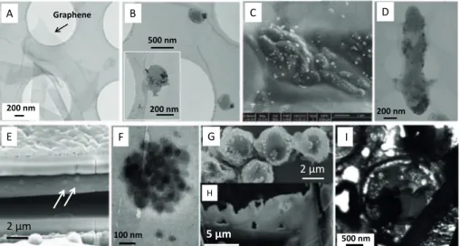
Figure 1: Electron microscopy images of light elements and soft matter materials. (A) A multilayer graphene flake; (B) magnetic beads (130 nm) attached to salt DNA
coils, white inset showing 40 nm beads; (C) A group of bacteria in a polymer matrix and (D) one bacterium at high resolution; (E) FIB-milled cross-section of a frozen wet hydrogel containing inorganic nanoparticles as indicated by white arrows whereas (F) one particle at HR, (G) Aspergillus niger spores at low resolution, (H) electron transparent lamella for TEM observation and (I) a TEM image of one spore where its cellular structure is visible. Panels (A, B, D, F) are taken at room temperature while (C, E, G-I) at cryogenic temperatures. Panels A, B, D, F and I are BF-TEM images whereas other panels are SEM micrographs.
In this thesis an experimental protocol has been developed to prepare water containing materials including biological specimens in the FIB for cryo-SEM observation. This technique is also used as a TEM sample preparation for high resolution imaging in the TEM (Figure 1G-I). Thus, cryo-FIB preparations can be discussed mainly in two parts: in the first part, large-volume specimens were investigated by cryo-SEM to optimize the ex-situ/in-situ FIB preparation process by preparing several specimens, e.g. bacteria and wet hydrogels (see Figure 1C-E). In the second step, TEM samples were prepared by extracting lamellae from the bulk and cryogenically transferred to a TEM for investigation. The FIB preparation for cryo-SEM observation was demonstrated on inorganic nanoparticle contained in hydrogels (paper VI) while cryo-TEM preparation on Aspergillus niger spores (Paper VII). For detail, see section 6.
1.2 Motivations and aims of the thesis
TEM has long history on low contrast and vacuum sensitive materials where specimens are prepared using advanced methods such as fixation and cryo-ultramicrotomy. Even if a long experience in the field has been accumulated, the TEM investigation of light elements and water-containing biological specimens is always a challenge. So, such materials always need specific microscope conditions and specific sample preparation techniques for their successful characterization.
The general aim and motivation of this thesis is to develop and refine TEM methodologies that enable us to study light elements and soft matter materials at high resolution. In addition, the techniques should be simple and less destructive but provide sufficient contrast for a successful visualization and interpretation.
The materials which have been investigated in this thesis are multilayer graphene flakes, DNA/magnetic nanoparticles and a number of hydrated biological specimens. In order to fulfill the aim, the work has been divided into three parts. (1) In the first part, a simple and fast TEM method for thickness characterization of graphene has been developed and applied to a large number of flakes. Graphene is a remarkable material due to its possible applications in different fields, e.g. in electronic devices, photonics and ceramics. However, to fully realize its applications high-yield production methods of graphene are needed. So, a quantitative TEM method was developed to measure thickness of large number of graphene flakes in order to control and optimize the conditions of the proposed method. (2) In the second part of this study, the interaction between DNA-coils and magnetic nanoparticles has been studied. Recently, new biosensors for the detection of different types of target biomolecules have been explored. Most of these sensors utilize nanoparticles and operate in a bio-molecular environment. In order to develop optimal sensors the details of the interaction of the nanoparticles with biomolecules must be understood. Therefore, TEM methodologies have been developed and refined to investigate DNA-bead interactions to obtain a better understanding of how different sizes of beads interact with DNA-coils.
(3) The third part concerns cryo electron microscopy studies of water containing specimens. The main aim and motivation of this study is to develop an experimental protocol to prepare specimens of hydrated biological samples for high resolution imaging in the TEM. Standard cryo preparation methods for TEM samples are not site-specific, i.e. it is not possible to choose a region of interest. In this thesis, a cryo-FIB technique in combination with SEM was developed to prepare site-specific regions of frozen hydrated specimens for TEM observation. In addition to this, the cryo preparation procedure and the related protocol for such specimens was optimized and improved. The method in fact offers the possibility to
investigate a bulk specimen with SEM at cryogenic temperatures and then choose regions of interest for FIB extraction anywhere on the surface of the sample with a precision in the sub-micrometer range for TEM observation. Our developed technique is novel that could open up vast new fields such as soft/hard matter interface related studies.
1.3 Thesis structure and outline
The thesis is organized in the following way. Chapter 2 presents a brief introduction to transmission electron microscopy (TEM) as well as different techniques which have been utilized throughout this work to characterize different materials. In addition, TEM sample preparation methods are also described briefly in this chapter. Chapter 3 presents a detailed description of the materials used. The next three chapters 4-6 are dedicated to material characterization by TEM and FIB/SEM methods. The microscopes are used both at room temperature and at cryogenic temperatures. The water containing biomaterial specimens are frozen with liquid nitrogen and characterized then by cryo-FIB/SEM and cryo-TEM. Chapter 4 presents TEM characterization of graphene flakes. In this chapter, a TEM method for fast thickness characterization graphene is described. The method is explained by presenting results from both simulation and experiments. Chapter 5 presents a study on attachment of magnetic nanoparticles to DNA coils where results of the TEM investigation are presented. In addition, the effect of surface coverage of oligonucleotides on immobilization of beads to DNA coils is studied by TEM. In order to locate the DNA coils in the TEM, the coils are labeled with gold nanoparticles of 10 nm. In Chapter 6, cryo preparation and characterization of frozen hydrated biological specimens is detailed. We described a novel technique that enables extraction of a thin lamella locally from a region of the bulk, the lamella subsequently thinned with the ion to electron transparency for high resolution imaging in the TEM. In addition, a detailed protocol of transferring of samples to a TEM is presented.
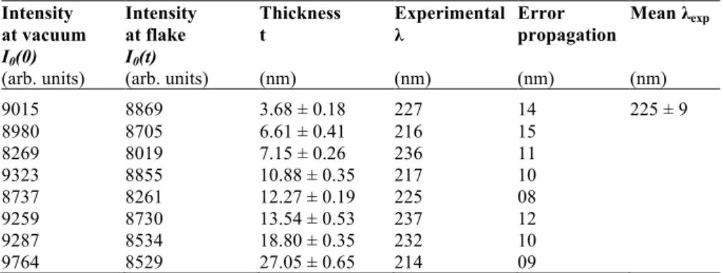
In paper I, the development of a TEM method for the thickness characterization of graphene flakes is presented. The method is elaborated by presenting results from both experiments and simulation and then applied to obtain thickness maps of graphene flakes. Papers II and III present the application of TEM thickness method (as discussed in paper I) to graphene by measuring the thickness of dozens of flakes. The flakes are produced using a wet chemistry method that results in flakes of a wide range of thicknesses and sizes. In paper IV, the attachment of magnetic nanoparticles to DNA coils is studied. The number of beads attached per DNA coil is estimated and the results of the TEM investigations are compared with magnetic measurements. In paper V, the impact of matrix properties on
survival of freeze-dried bacteria is characterized by SEM. In paper VI, a preparation protocol for wet biomaterial specimens is developed and samples of wet hydrogel are characterized by cryo-SEM. The SEM image quality at liquid N2 temperatures allowed analysis of inorganic nanoparticles in particular concerning the grain location and grain size. In paper VII, a site-specific FIB lift-out method for cryo-TEM studies is developed. The method is demonstrated on spores of Aspergillus niger frozen by plunge freezing in liquid N2. Thereafter, the samples are transferred to an Alto 2500 prep-chamber and then a FIB/SEM. A nano-manipulator is modified to be cooled during the in-situ lift-out process in the FIB. Once the lamella is thinned to electron transparency, it is transferred cryogenically to a TEM using a custom-built cryo-transfer bath. The sample is studied then at cryogenic temperatures by BF/DF, HR and EFTEM methods.
2
Transmission electron microscopy
In this chapter an introduction to transmission electron microscopy (TEM) and related methods is given, with an emphasis on to methods for light and soft materials. A broader and, to some extent more detailed description is given in Williams and Crater [21] and Reimer [32]. Materials analysis in the electron microscope is based on the interaction of electrons with matter and the various kinds of signals generated. In a Scanning Electron Microscope (SEM) a narrow beam is raster-scanned over a bulky specimen; an image of the sample surface is constructed pixel by pixel by measuring the secondary or backscattered electrons. In a Transmission Electron Microscope (TEM), a broad beam passes through a thin sample producing an image due to diffraction or mass-thickness contrast. This image is subsequently magnified by a set of electromagnetic lenses and recorded on a photographic film or CCD camera. It is possible to investigate both materials science and life science specimens at high resolution in a TEM. The main TEM techniques used in this thesis include bright-field (BF) imaging, dark-field (DF) imaging, high resolution (HR) imaging and electron diffraction (ED). Thus in this work mainly signals arising from elastic scattering are used. A photograph of the microscope used in this thesis is shown in Figure 2.
In a TEM, normally those electrons are analyzed which are transmitted through the sample. These electrons are emitted by the electron source situated at the top of the microscope column and accelerated towards the specimen using a positive electric potential. These are called primary electrons. On the way to the specimen, the beam of electrons is condensed by the first and second condenser lenses, respectively C1 and C2. Both lenses have apertures known as condenser apertures which are used to block the electrons that propagate through the column at angles higher than a specific value. Both C1 and C2 are above the sample along with their apertures. The fast electrons then interact with specimen. Samples are usually prepared to be thin enough so that the electron beam can pass through without losing too much intensity (the thickness should be between 0.3 and 0.7 mean free paths). After interaction with the sample, the electrons that are transmitted through the specimen are focused by the objective lens to form an image. The objective aperture can be used to select either direct or scattered electrons that can contribute to the image. A series of lenses are used below the specimen to magnify both ED patterns and images. The
thickness of the TEM samples used in this work ranges between 5 nm and 300 nm.
Almost all kinds of materials can be characterized by using TEM. Today, many techniques based on imaging, spectroscopy and diffraction are used depending on the specific analysis requirement for each sample. This work, with the use and refinement of imaging and diffraction techniques, can contribute to the development of novel methodologies to study light elements and soft matters including frozen hydrated biological specimens. Two types of TEMs operated at 300 and 200 keV respectively have been utilized in this work: 1) the first microscope is a FEI Tecnai F30ST TEM operated at 300 keV (see Figure 2). This microscope is equipped with a field emission gun (FEG), a post column spectrometer, a Gatan image filter (GIF) and a 2048x2048 pixel CCD camera. 2) The JEOL JEM-2000FXII equipped with a LaB6 thermionic emission electron gun operated at 200 keV has been used for BF/DF imaging and selected area electron diffraction (SAED) experiments. In some cases it has been also used for HR-TEM imaging. This microscope provides easy access and simple recording of images on negatives and CCD camera.
Figure 2. Photograph of the main microscope used in this thesis: FEI Tecnai F30
TEM with field emission gun (FEG), situated at the Ångstrom Laboratory, Uppsala University. (October 2011).
2.1 Brief historical background
The first postulate about the wave-like behavior of electron with a wavelength much shorter than visible light was given by Louis de Broglie in 1925 [33]. Two years later, Davisson and Germer [34] and Thomson and Reid [4] experimentally proved the wave nature behavior of electrons by conducting electron diffraction experiments on a nickel crystal and a gold foil. After having developed electron lenses, Ruska and Knoll built a first electron microscope in 1931 [35]. The major development in material science came about in the 1940s when Heidenreich (1949) introduced for the first time a routine method to produce TEM samples. In addition to that he discussed the electron diffraction phenomena and gave the concept of kinematical diffraction theory for interpreting the images of crystalline materials [36]. Later, Cambridge University groups developed the theory of electron diffraction contrast to determine possible crystal structures [37]. Historically, TEMs were developed since the image resolution of optical microscopes is limited by the wavelength of light. If relativistic effects are ignored then de Broglie’s equation takes the form λ~1.22[nm.eV1/2]/E1/2[eV1/2], which shows that the wavelength of electrons
(in nm) is related to their energy, E (in eV) [3]. For example, for 200-keV electron, λ = 0.00251 nm which is much smaller than the size of an atom (0.1-0.5 nm) [1]. Since the 1970s, many TEMs have been developed to resolve individual rows of atoms in the crystals by high resolution imaging [7]. Due to its low mass, the electron can be deflected easily by the nucleus or the electrons of an atom. The scattering of particles due to electrostatic interactions known as Coulomb interactions or forces is the main process used in TEM imaging techniques. It is important to note that the electron beam can be treated in two different ways. In electron scattering, it is considered as a particle while in electron diffraction it is treated as a wave. The scattering probability of the electron can be explained by the concept of cross-section and mean-free path [38]. There are principally two forms of scattering; elastic (no loss of energy) and inelastic (loss of energy). Both forms are useful for the analysis of samples but the latter has the side effect of being responsible for specimen damage. Beam damage is more severe for light elements and soft matters and ultimately limits applicability of the TEM analysis to such samples [11, 12].
2.2 Sample preparation
Sample preparation is an important part of the TEM characterization [39]. It is important to use or develop a preparation technique that does not change the properties of the samples under study. For high resolution imaging, very thin samples are needed, 20-80 nm in thickness [39], whereas in the case of
biological specimen a couple of 100 nm thickness is also electron transparent [40]. The TEM techniques used to prepare such thin sections or thin foils depends on the materials under analysis. For example, the large-volume frozen hydrated biological specimens are prepared by focused ion beam (FIB) prior to transfer to TEM. For this purpose, a cryogenic dual beam FIB/SEM microscope with a Gatan Alto 2500 chamber and a custom-built transfer station can be used. This dedicated technology offers the possibility to prepare frozen biological specimens for cryo TEM studies at atomic scale resolution. A detailed discussion of this topic can be found in Chapter 6. The samples of Aspergillus niger spores, gold labeled DNA, inorganic nanoparticles in hydrogels, and bacteria/polymer matrix were prepared by using this technology. However, the materials that have dimensions small enough to be electron transparent, such as nanoparticles, powders, graphene flakes or DNA molecules, can be prepared by depositing a dispersion containing materials onto TEM grids.
Figure 3. Micrograph of a TEM grids used in this thesis for TEM experiments: (A)
In the optical microscopy photograph, the meshes of the grid (squares) can be seen; (B) SEM image of a part of a mesh shows the holes in the carbon film (black solid circles).
The graphene flakes were collected by dipping the TEM copper grids into the solution used during ultrasound assisted exfoliation. The method is called deposition. After deposition, the grids were dried in air and stored in special TEM boxes prior to loading in the TEM. The specialty of these grids is that they have very thin (8-30 nm) support amorphous carbon films with holes. The holes in the carbon provide the possibility to get suspended flakes in vacuum and obtain high resolution images of folded edges of graphene layers. The carbon film itself is useful to support the flakes or nanoparticles. This kind of grids has been extensively used in this thesis and example of such a grid is shown in Figure 3, where the solid circles in black contrast are the holes in the C-foil (panel B). The DNA/bead samples were prepared by pipetting a small amount of solution onto TEM grids instead of dipping (again the process is called deposition). Through-out this work the TEM
samples were prepared by both ways, i.e. cryo-FIB/SEM method and deposition method.
In summary, after preparation of samples, a FEI Tecnai F30 TEM operating at 300 kV was used for graphene characterization (Papers I-III). The DNA/magnetic nanoparticle materials were studied by JEOL JEM-2000FXII TEM operating at 200 kV (Paper IV). The freeze-dried Pseudomonas putida (rod-shaped bacteria) and nanoparticles in hydrogels were studied by FEI Strata DB235 cryo-FIB/SEM (Papers V-VI) whereas samples of Aspergillus niger spores were prepared by cryo-FIB/SEM and studied by a FEI Tecnai F30 TEM (300 kV) (Paper VII).
2.3 Electron diffraction
Before discussing on electron diffraction (ED), it is important to first note some differences between electrons and X-rays, i.e. 1) electrons are negatively charged particles whereas X-rays are neutral, 2) electrons have a much shorter wavelength than X-rays, 3) electrons are scattered/diffracted more strongly than X-rays through Coulomb forces, 4) due to their charge, electrons can be directed and accelerated at very high velocity towards the specimen by applying a potential. Diffraction is a phenomenon where the wave nature of electrons and photons is most evident. ED occurs when electron waves interact with atoms; generally this effect is stronger when the wavelength of the waves is of the order of or smaller than the size of the encountered objects. The diffraction patterns are formed due to constructive and destructive interference between the various diffracted waves. The ED can be used to study the crystalline materials and derive their structure. In crystalline materials, the spacings between atomic planes are characteristic of their structure. In this section the wave nature behavior of the electron is discussed where the electron interacts with the sample and is diffracted into different angles. The formation of electron diffractogram in the TEM is described briefly. To understand the diffraction contrast of TEM images and the intensity of the non-diffracted beam and diffracted beams, a detailed discussion of the electron diffraction is given where kinematical and dynamical diffraction theories are discussed.
2.3.1 Formation of electron diffractogram in the TEM
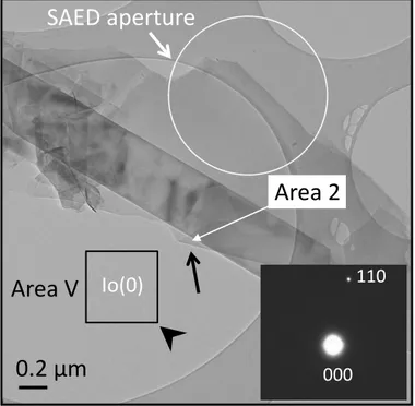
In order to form the ED diffractogram in a TEM, the strength of the intermediate lens is altered so that it projects onto the fluorescent screen the back focal plane (BFP) of the objective lens. This diffracted pattern is recorded on negative films or a CCD camera. The non-diffracted beam, which by definition passes straight through the sample, is represented by the central (usually brightest) spot in the diffraction pattern. ED spots are
formed in the diffraction plane of the objective lens by those electrons which are scattered by the same scatter angle. On the contrary, the image is formed in the image plane of objective lens by electrons coming from the same point of the sample (see Figure 4). A detailed discussion can be found in [21].
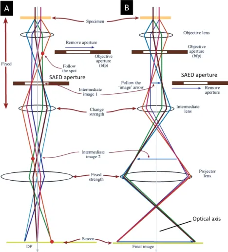
Figure 4. A schematic illustration of different electron beams along with lenses and
apertures in the TEM to perform ED (A) and imaging (B). In both cases, the sample is shown on the top where parallel electron beam is incident on it. After passing through the sample, the electron beam splits into several beams due to Coulomb interaction and is guided through the lenses and aperture before being focused to the screen. The important parameter is the current of the lens lying immediately below the objective lens (intermediate lens). A reduction (or increase) in the flow of current will reduce (or increase) the focusing power of the lens and projected to the next lens the bfp (panel A) (or the image plane (panel B)) of the objective lens as its object. Subsequently, the projection lens focuses the electrons to the screen to produce a diffraction pattern (or image) of the sample. In order to select a small area of the sample, an aperture called SAED aperture can be inserted in image plane of the objective lens to obtain a SAED pattern for nano-objects.(Adapted from ref. [21] and reproduced with the permission of SPRINGER publishers).
An ED pattern shown in Figure 4 contains electrons that are scattered in a limited volume of the specimen that is defined by the size of the aperture known as selected area electron diffraction (SAED) aperture and the operation is called SAED. This operation of ED is very useful to study specific regions on the sample. The SAED operation is obtained by inserting a SAED aperture in the image plane of the objective lens. The image of the aperture can be seen and centred on the fluorescent screen i.e. centre of the optical axis. Insertion of this aperture, removes all those electrons from the image plane which hit outside the diaphragm of the aperture stops them to contribute to the diffraction. The size of the aperture defines thus the area of the sample from which the diffracted electrons are selected. SAED apertures in different sizes are available that enables us to analyse nanometre sized objects. The SAED patterns are displayed on the viewing screen at a magnification given by the camera length. This distance corresponds to the distance of the recording film or CCD camera from the diffraction plane of the objective lens.
2.3.2 Kinematical electron diffraction
In crystalline materials, the interaction between incident electrons and atoms occurs at the atomic site due to the combined effect of the nucleus and the electrons of the atom. The scattering probability depends on the crystal structure and the spatial distribution of electrons in the atom [41]. So, when electrons propagate through a family of lattice planes, then they are either scattered at some angle (scattered/diffracted beams) or pass through the sample along their initial trajectory (direct beam). However, the electrons that are diffracted into a beam can be diffracted again into another direction. The process can continue in a similar way due to strong Coulomb’s forces even for samples that are only 10 nm thick. This repeating or multiple scattering of beams is known as dynamical or plural diffraction while a single event of diffraction is termed as kinematical diffraction. The Bragg condition describes kinematical diffraction theory as discussed below. If, during scattering, the electrons do not lose their energy, the process is called elastic scattering otherwise it is known as inelastic scattering. Note, in this section only elastic scattering is considered.
The Bragg’s law is a very useful tool to understand the diffraction phenomenon in crystalline materials; in fact it tells that the construction interference occurs when the path difference between two diffracted waves is an integral multiple of the wavelength, i.e.
,
sin
where d is the inter-planar spacing of atomic planes, ӨB is the scattering
angle, λ is the wavelength of the electrons and n is an integer. So, the observed intensity of bright spots in the diffraction patterns is the results of the constructive interference of the diffracted beams that depends on several factors, e.g. d, λ and the angle of crystal orientation with respect to the incident electron beam.
The electron diffraction patterns in a TEM can be understood and interpreted with the concept of reciprocal lattice. Every crystalline material has two types of lattices, one real and the other reciprocal. The reciprocal lattice structure is always related to the real lattice by a Fourier transformation. In order to understand the reciprocal lattice, few terms are discussed here. We introduce the wave vector transfer K:
.
sin
2
:
λ
θ
B=
K
(2.2)K is a change in k-vectors, i.e. KD-K0, where |K0|=1/ λ is the incident wave
vector and KD is the scattering vector; their direction is the same as the
direction of propagation of the respective beams. For a scattering angle ӨB (Bragg angle) the electron waves interfere constructively. So, at Bragg angle, from eq. (2.1) and n=1 the magnitude of K has the value KB, i.e.
,
:
1
g
d
B=
=
K
(2.3)where g is the reciprocal lattice vector.
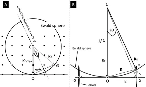
The Bragg law is not only useful to relate real and reciprocal space, but it explains also the process of diffraction by giving a pictorial representation where diffracting atomic planes appear to behave as mirrors for the incident electron beam. Therefore, the diffracted beams or the spots in the ED patterns are often called reflections. The vector g is called the reciprocal lattice-vector or the diffraction vector which is normal to the lattice planes. This means that K is parallel to this normal and the angles of incident scattering ӨB of the lattice planes must be equal (see Figure 5). It should be noted that, for real samples, each point of the reciprocal lattice is associated with the reciprocal-lattice rod, known as simply relrod. The rods are due to the finite thickness of the TEM specimen. Equation (2.3) can be used to construct a sphere with radius 1/λ known as Ewald’s sphere, first employed by Ewald. The combination of the concept of reciprocal lattice, relrod and Ewald sphere can be used to understand the intensity of the ED spots, i.e. how it varies with specimen tilt and direction of incident electron beam.
Figure 5. Illustration of ED patterns with the concepts of reciprocal lattice and
Ewald’s sphere. (A) The diffraction spots are originated when the Ewald’s sphere intersect the reciprocal lattice points in the exact Bragg condition; K0-KD=g where
incident vector, CO=K0 and diffracted vector CG=KD terminate on the sphere with
lengths equal to radius of the sphere, 1/λ. O is the origin of the reciprocal lattice and C the center of the sphere. If the radius of the sphere is of the same order as the distance between the reciprocal points (as it is the case for X-rays) then the sphere can only intersect a few points. (B) When λ is much smaller, as for 300 keV electrons, the radius is much larger, the sphere is flatter, and it cuts through many more points. The OG=g is a Bragg reflection vector whose head is connected to the head of the scatter vector KD, the new vector s = |GQ| is called an excitation error. It
should be noted that even with s, the reciprocal spot is still excited (with a faint intensity) as Ewald’s sphere cuts the relrod at Q whereas the same spot will have its maximum intensity (for Bragg condition) at G (center of the relrod).
Consider an origin of the reciprocal lattice O as one end of the vector CO=K0 where K0 is the wave vector of the incident electron beam. The
second end of this vector C is called excitation point of K0 is taken as a
center of a sphere of radius 1/λ. The important point is that the diffraction spots will be observed only at scattering angles where the Ewald’s sphere cuts one or more g (e.g. G in Figure 5A) of the reciprocal lattice. The Ewald’s sphere has a short radius for X-rays, as shown in Figure 5A. The intersection points on the Ewald’s sphere appear brighter in the diffraction patterns. It should be noted that for X-rays only few points will be excited in Bragg condition as the sphere is of small radius due to longer wavelength and it cuts therefore only few lattice points. However, energetic TEM electrons have shorter wavelength and hence the sphere is very flat and cuts through many points (Figure 5B). For example, the radius of the sphere for 0.2 nm X-rays is 5 nm-1 and 508 nm-1 for 300 keV electrons, much bigger than the distances between the reciprocal lattice points of graphite (0.335
nm), e.g. 1/d ~3 nm-1. In addition as TEM specimens are very thin so reciprocal lattice points turn to rod-like shapes (called relrod); therefore even when the sphere cuts through a relrod the diffraction spots will have some intensity, even though the Bragg condition is not strictly satisfied. Thus, there are many points excited in the electron diffraction patterns (see Figure 6B, C).
According to eq. (2.1), i.e. 2sinӨB = nλ/d, the Bragg scattering angle is inversely related to the distance between the lattice planes. This means that the reflections of larger inter planar spacing (d) appear closer to the direct beam and reflections with smaller d far away, i.e. at larger angles. The rings round the direct beam in the ED pattern reveals that the sample has several grains in the region from where pattern has been taken while discrete spots means fewer grains [42]. The magnification of ED patterns is described by a term called camera length (L). The d for each Bragg reflection then can be found by the simple relation, R. d=L. λ using Bragg’s law and Figure 6A; where R is the distance of reflection from the central spot, λ is the wavelength of the incident electron beam and L is the camera length of the microscope.
Figure 6B, C shows electron diffraction patterns of two samples, graphene sheets and hydroxyapatite (HAP) nanoparticles, respectively taken by TEM. The central part of both the patterns is brighter as indicated by X in panels B and C and represents those electrons which are transmitted through the sample without any significant deviation from the initial direction. The other spots are the intensities of diffracted beams. Note that the diffraction pattern in panel B shows discrete spots, this means that the sample has one larger grain of graphite. Contrary to this, the second pattern (panel C) has several spots with same distances from the central spot. This reveals that in the different HAP particles, same lattice planes have different orientations.
The intensity of the diffracted beam Ig (t) can be calculated by using the
column approximation in two beam case. The column approximation is discussed in appendix [43].
,
)
.
(
)
.
.
(
sin
)*
(
)
(
)
(
2 2 2 2s
t
s
t
A
t
A
t
g g g gπ
π
π
ξ
=
=
Ι
(2.4)
where ξg is the extinction distance for particular reflection which oscillates
with increasing thickness, s a small deviation from the exact Bragg condition called excitation error (see Appendix) and t is the thickness of the specimen. Ag (t)* is the complex conjugate of Ag (t). If the Bragg condition is exactly
satisfied, i.e. s=0, then the diffracted intensity can obtain from eq. (2.4) as Ig
(t) = π2t2/ ξ
g2. It can be seen that this intensity increases as t2. If s ≠ 0, the intensity Ig (t) oscillates with increasing t and reaches the maximum value (1/
s>>1/ ξg. This is valid only for very thin samples; for which diffracted intensity is small and the reduction in the direct beam intensity I0(t) can be
neglected (see Figure 5B legend). This condition is called kinematical theory that is valid only for thin samples.
Figure 6. (A) The spacing R i.e. the center-to-center distance of direct beam and
diffracted beam intensity assuming intensity as a Gaussian distribution is related to the camera length, L, d and λ. At constant L and λ, R depends only on d where it can be magnified through a system of lenses and moving the recording screen further. ED patterns of single crystal (B) and poly-crystal (C) materials which contain information about the crystal structure and d of the crystal lattice. Direct and one diffracted beams in each case are highlighted by a cross sign and a white circle respectively. The beam stopper is indicated by an arrow.
When an electron interacts with an isolated single atom, it can be deflected in several fashions with certain angle. In case of diffraction patterns, the scattering semi-angle 2Ө (scattering angle) is defined by the objective aperture and the direction of the incident electron beam which is in the range of milliradians (mrads). The scattering event is influenced by certain factors such as energy of the incident electron beam and the atomic number of atom. When considering specimens, i.e. many atoms instead of single atom, then the scattering event will be more complex and depending on many factors, e.g. 1) specimen thickness, 2) material density, 3) structure of the specimen, and 4) the angle of specimen to the incident beam. A detailed study of scattering or diffraction theory is needed to fully understand these factors which are discussed in the next section.
2.3.3 Dynamical electron diffraction
The multiple scattering of the electron beam by the crystalline planes of atoms of the specimen is known as plural or dynamical electron diffraction. The formulation of dynamical theory was used for the first time for X-rays diffraction by Darwin (1914) [44] later adapted to electron diffraction by Howie and Whelan (1961) [45]. In dynamical diffraction, the intensities of the primary beam and the diffracted beams oscillate within the specimen with increasing thickness. The dynamical theory addresses the interaction between primary beam and diffracted beams whereas kinematical theory describes approximate positions of Bragg spots of diffraction patterns. When an electron beam enters the crystalline specimen it will split into direct and diffracted beams. The total wave function passing through the crystal is a sum of all the beams where each wave has an appropriate phase factor. To simplify the situation of many beams, consider an important case where only one Bragg reflection is excited, known as two-beam approximation, including the primary beam with g=0. Two-beam condition means that the crystal is tilted with respect to the incident electron beam such that there is only one diffracted beam strongly excited (s=0), whereas the other beams are very weak (s≠0) and therefore their contributions are negligible. In this case, both intensities exhibit then sinusoidal behavior with increasing thickness.
In order to bring out the most important results of the dynamical theory, the two-beam case is considered. We assumed that a direct wave of amplitude A0 (t) and a diffracted wave of amplitude Ag (t) fall on a layer of
thickness Δt (where t is the total thickness of the specimen) inside the crystal. After passing through the foil the amplitudes of both the waves will be changed. The changes in intensity at a point just below the specimen are calculated using the column approximation method (see Appendix) [43]. The result is a linear system of two differential equations called Howie-Whelan equations given by Howie and Whelan for electron diffraction that can be extended to n-beam case [46]. It can be stated that A0 (t) and Ag (t) are
‘dynamically coupled’. The term dynamical diffraction thus means that the amplitudes and therefore the intensities of the direct and diffracted beams are constantly changing, i.e., they are dynamic. Finally, the diffracted intensity Ig
(t) at point P, assuming incident intensity I0 (0)=1 can be represented as [43].
)
1
(
sin
1
1
)*
(
)
(
)
(
2 2 2 g g g gt
w
w
t
A
t
A
t
ξ
π
+
+
=
=
Ι
Figure 7. A schematic shows the direct and diffracted beams at exit point P. When a
beam of incident electrons strikes the crystalline sample then a part of it is scattered and the rest is un-scattered. Both types of beams then come out from the specimen at the bottom of the surface as a direct beam (O) and a number of diffracted beams (Gi). These sets of reciprocal points then contribute to the image when combined by the objective lens.
Now the intensity I0 (t) = A0 (t) A0 (t)* of the direct beam, which is referred
as the transmission T and the intensity of the reflected beam Ig (t) = Ag (t) A0
(t)*, referred as the reflection R are calculated. Both intensities; T (where T is the ratio of the direct beam I0 (t) to incident or primary beam intensity I0
(0)) and R through the specimen of thickness t can be related by the following expression as:
)
1
(
sin
1
1
1
2 2 2 gt
w
w
T
R
ξ
π
+
+
=
−
=
,
(2.5)
The parameter, w (=s ξg) appearing in eq. (2.5) is called the tilt parameter out of the Bragg condition (as for Bragg condition, s = 0; this implies that w = 0). It can be seen that the electron intensity oscillates between primary beam (T) and Bragg diffracted beam (R) with increasing thickness t of the dynamical theory. For example, for w>>0 (large tilt out of Bragg condition), w 2 + 1 ≈ w 2 = (s ξg) 2, the eq. (2.5) becomes,
.
)
.
(
)
.
.
(
sin
1
2 2 2 2s
t
s
T
R
gπ
π
ξ
π
=
−
=
(2.6)
It should be noted that the expression for kinematical theory (i.e. eq. 2.4) and dynamical theory (i.e. eq. 2.6) leads to identical results. However, at Bragg
condition (s = 0), the kinematical theory shows that Ig (t) increases with t2
and becomes larger than 1 (intensity of primary beam), which contradicts the law of conservation of intensity T + R = 1. So, eq. (2.5) for the exact Bragg condition (w =0) can be re-written as,
).
.
(
sin
1
2 gt
T
R
ξ
π
=
−
=
(2.7)
Figure 8. Pendellösung fringes of the dynamical electron diffraction theory. In
two-beam case without absorption, the intensity of the primary two-beam (assuming maximum to 1) oscillates between T (direct beam) and R (diffracted beam).
It can be seen that the law of conservation holds for this expression where R and T are oscillating with increasing t by changing their intensity from one to the other but the total intensity remains constant (see Figure 8). This means that for Bragg condition, the electron intensity oscillates between the direct and the Bragg reflected beam with increasing film thickness. Now it is easy to explain the concept of the extinction distance ξg which is the oscillating period. T will have maximum value when
g g g
n
t
n
t
t
ξ
π
ξ
π
ξ
π
=
⇒
=
⇒
=
0
(
)
)
(
sin
2,
(2.8)
where n is an integer (n = 0, 1, 2 …). Eq. (2.8) is a very useful result that can help to understand the situation when an electron beam is incident to the specimen. Three different cases are discussed to explain the intensity of diffracted beam R and direct beam T: (1) when the thickness of the specimen is comparable to (n+1/2) ξg, then all the intensity will appear as R whereas, (2) for t = nξg, it will be totally transmitted as T in the direction of the
incident beam, (3) for values of thickness other than (1) and (2), the intensity will be distributed in both T and R. It is important to mention that these are the possible situations when no absorption is present in the system, i.e. T + R = 1 (=I0(0)) is satisfied. However, in case of absorption this
condition will no more apply and both T and R will go to zero after a certain thickness. So the following analytical formula for T can be derived for the two-beam case with absorption [47],
⎥ ⎥ ⎥ ⎥ ⎥ ⎦ ⎤ ⎢ ⎢ ⎢ ⎢ ⎢ ⎣ ⎡ + + + ʹ′ + + + ʹ′ + + = ʹ′ − ) * 2 1 cos( ) ) 1 * 2 sinh( 1 2 ) ) 1 * 2 cosh( ) 2 1 ( ) 1 ( 2 2 2 2 2 2 2 * 2 0 g g g t t w w t w w w t w w e T
ξ
π
ξ
π
ξ
π
ξ π(2.9)
where ξ0´ and ξg´ are the mean and anomalous absorption distances respectively.
Anomalous absorption is the difference between the interaction probability for the waves with nodes and antinodes at the nuclei due to inelastic scattering. Eq. (2.9) is a very important and useful expression to calculate the intensity of transmitted beam (as in the case of BF imaging) to estimate the thickness of the specimen (see section 4).
2.4 Bright-field and dark-field imaging
In the TEM when a beam of electrons of high energy strikes a thin sample then most of the electrons pass through it. These are called transmitted electrons and include both undeflected and deflected electrons. The beam of electrons which passes through the sample without any deflection from its original direction is focused at the back focal plane (BFP) of the objective lens parallel to the optical axis and is called direct beam. The other electrons which are scattered at certain angles are focused off-axis at the BFP of the lens and they are called diffracted beams.
In order to form images in the TEM from transmitted electrons, either the central bright spot, or some or all of the scattered electrons can be used. Electrons scattered at a specific angle can thus be selected by inserting an aperture into the BFP of the objective lens. This aperture is called the objective aperture (see Figure 9). If the direct beam is selected (Figure 9A), the resultant image is called bright-field (BF) image, and if scattered electrons (Figure 9B) are selected then the micrograph is called dark-field (DF) image. Typical magnification ranges of these modes are 25,000x-100,000x. An example of a BF and DF image is shown in Figure 10.
Figure 9. The two schemes show how the direct and diffracted beams can be
selected to form an image. The objective aperture is used to remove either the diffracted beam (panel A) or the direct beam (panel B) from those electrons which contributed to the image. If direct beam is allowed to pass through the aperture then it is called bright-field (BF) imaging, whereas an image formed by selection of a diffracted beam is known as a dark-field (DF) image. The direct beam is focused on the optical axis (OA) parallel to the incident beam whereas the diffracted beams are always off-axis. The objective aperture is shown by a black solid circle where one spot is selected (white solid circle) in each case. Without aperture all five spots would appear on the screen. The plus sign represents the optical axis of the microscope.
The intensity and contrast of the BF/DF images mainly depends on three factors: atomic number (Z), thickness and structure (amorphous or crystalline structure) of the sample. The regions of the sample containing heavy elements and/or thick will scatter more electrons and appear darker in BF and vice versa in DF imaging mode. In such cases the probability of electron scattering is high due to larger atomic cross-sections and shorter mean free paths. The samples containing light elements (e.g. H, C, O, N) including biological specimens scatter little amount of electrons: consequently the contrast or intensity difference between regions containing different light elements is smaller. Additionally, the bombardment of
electrons can damage such specimens very quickly which puts considerable limits on the exposure time and requires an optimization of the electron dose each sample receive during imaging.. It is worthwhile to mention that the electron beam damage can be reduced to some extent by operating the microscopes at cryogenic temperature. This technique is called “cryo transmission electron microscopy” specifically used for hydrated biological specimens (as discussed in Chapter 6).
Figure 10. TEM micrographs of gold labeled DNA-coils in bright-field (A) and
dark-field (B) imaging modes. The contrast seen in panel A is inversed in panel B. The difference in contrast between BF and DF can e.g. be observed on the place marked by an arrow. Note that the substrate is a holey carbon film.
Figure 10 shows TEM micrographs of gold (Au) nanoparticle labeled DNA coils acquired in BF and DF imaging modes. The holes in the carbon films (vacuum) appear brighter in the BF than the rest of the sample since they scattered no electrons (panel A). The darker spots in the image are the DNA coils; here the contrast of the DNA was reinforced by the presence of a heavy Z-number element, Au in this case. The spots of DNA coils are clearly visible in this magnification where each coil is labelled with 10 nm Au nanoparticles. In the BF image, the coils appear with a darker contrast than carbon film since gold has a higher elastic scattering cross-section than carbon because of the lower Z number. Therefore, Au scatters more electrons and appears darker than the carbon background in the BF image. In contrast, the DNA/Au show brighter contrast and holes are darker in the DF image (panel B). In order to see the difference in contrast, the same spot is pointed out by an arrow in both images, the spot which was dark in panel A turns to a bright spot in panel B.


![Figure 13. (A) Every mark of a lead pencil can include a small quantity of graphene which has become a remarkable material in science and engineering, Matt Collins [54]](https://thumb-eu.123doks.com/thumbv2/5dokorg/5471122.142354/44.701.94.600.172.510/figure-include-quantity-graphene-remarkable-material-engineering-collins.webp)