School of Innovation Design and Engineering
Västerås, Sweden
Thesis for the Degree of Master of Science in Engineering - Robotics
DVA502 30.0 credits
LOW COST ULTRA WIDEBAND
RADAR FOR HUMAN PROTECTION
Martina Öhlund
mohlund0@gmail.com
Hampus Carlsson
hcn10002@student.mdh.se
Examiner: Magnus Otterskog
Mälardalen University, Västerås, Sweden
Supervisor: Martin Ekström
Acronyms
ADC Analog-to-Digital Converter. BJT Bipolar Junction Transistor.
CMOS Complementary Metal Oxide Semiconductor. EMC electromagnetic compatibility.
EMI electromagnetic interference.
ESS-H Embedded sensor systems for health. LNA Low Noise Amplifier.
MCU Microcontroller Unit.
MOSFET metal oxide semiconductor field effect transistors. PAM Pulse-amplitude modulation.
PCB Printed Circuit Board. RF Radio Frequency. SRD Step Recovery Diode. UWB Ultra Wideband.
Abstract
The majority of the UWB radars available on the market today are expensive and often closed for further development due to proprietary rights. Therefore it is difficult to fully understand and adapt the functionality of an available UWB system to fit one’s needs. The consulting-firm Addiva purchased an UWB radar to be used in a safety system. However, the radar had limitations and the functionality of it was partly unknown. This master thesis was inspired from this issue to examine the possibilities of developing a low-cost UWB radar, with main focus on research of human detection. The system should be easy to understand and modify, as well as reporting reliable data from the scanning. The results indicate that such a system can be developed. However, further development to the UWB radar needs to be made in order to have a complete system.
Sammanfattning
Majoriteten av de befintliga UWB radarsystemen som finns på marknaden idag är dyra och ofta begränsade för viderutveckling på grund av äganderätt. Detta leder till komplikationer att få en full förståelse över funktionaliteten i ett befintligt UWB system och att anpassa den efter ens behov. Konsultbolaget Addiva införskaffade en UWB radar för användning i ett säkerhetssystem. Denna radar hade dock begränsningar och viss del av funktionaliteten var okänd. Det här examensarbetet inspirerades utifrån dessa problem att undersöka möjligheterna för att utveckla en lågkostnads-UWB radar, för användning främst inom forskning för detektering av människor. Systemet skall vara lätt att först� och modifiera, samtidigt som det ska ge tillförlitlig data från scanning. Resultaten av denna rapport indikerar att ett sådant system kan utvecklas. Vidareutveckling av systemet behövs dock, för att ett komplett fungerande system skall erhållas.
Table of Contents
Acronyms 1 1 Hypothesis 5 2 Problem formulation 5 3 Introduction 6 4 Background 7 4.1 Pulse generator . . . 8 4.2 Pulse shaper . . . 8 4.3 Amplification / transmitter . . . 9 4.4 Antenna . . . 9 4.5 Amplification / receiver . . . 9 4.6 Sampler / Integrator . . . 94.7 State of the art . . . 10
5 Method 11 6 Hardware 12 6.1 Testing . . . 12 7 Transmitter 13 7.1 Pulse Generator . . . 13 7.1.1 Pulse Generator V1.0 . . . 13 7.1.2 Pulse Generator V1.1 . . . 15 7.1.3 Pulse Generator V1.2 . . . 16
7.1.4 Miscellaneous Pulse Generators . . . 16
8 Receiver 19 8.1 Pulse Amplification . . . 19
8.2 Pulse matching . . . 19
8.2.1 Advanced Gilbert Cell . . . 20
8.2.2 Basic Gilbert Cell . . . 21
8.3 Pulse Extender . . . 22
9 EMC 23 9.1 EMC Issues in this project . . . 24
10 Results 25 10.1 Q1: What are the drawbacks of a low cost UWB radar? . . . 25
10.2 Q2: Will the bottleneck be in software or hardware? . . . 30
11 Discussion 31
12 Future Work 33
1 Hypothesis
The hypothesis for this thesis work is as follows:
A simple low cost Ultra Wideband (UWB) radar for human detection can be developed.
In order to develop a low cost system, each module should be assessed and made from scratch to evaluate where the cost can be reduced. This will result in the development of a simple and easily understandable system, which allows for further development of the UWB radar.
The problem formulation (Section 2) evaluates this hypothesis and focuses on the possible challenges with it.
2 Problem formulation
In order to make a low cost UWB radar, some questions need to be answered. This section discusses the main challenges that emerges when developing a UWB radar:
Q1 What are the drawbacks of a low cost UWB radar?
One of the challenges of making the system low cost is that it is time consuming. As there is no low cost chip available, see Section 4.7 for more information, the electronics need to be built from scratch. This results in that each sub circuit needs to be tested thoroughly to ensure a properly working system.
This leads to the question of whether or not it will be possible to decide if a reasonably low cost UWB radar can be made within the given time frame. A prototype will be developed during this period, where the quality of it may vary. However, there will at least be some groundwork on the subject, which can be further researched in the future. It should also with this information be possible to roughly decide the probability of developing a successful low cost UWB radar. Another concern about making it low cost is if it heavily affects the precision of the UWB radar. Will the function of some sub circuits be affected by the fact that it is low cost and therefore not being able to perform as well as a more expensive solution? The strength for high frequency signals declines rapidly with longer distances on the circuit board. Therefore this could be a problem with a low cost solution as more components will be present on the circuit board.
Q2 Will the bottleneck be in software or hardware?
Some functionalities are better to implement in software, other in hardware. Some parts will be restricted due to the limited development time while other parts will restrict the final product. It is therefore difficult to pinpoint the bottleneck as it depends on how and what is being evaluated. For example, when developing, it will most likely be the development of the hardware that is most time consuming and therefore acts as the bottleneck. In the final prototype, however, it may be the software that slows down the system compared to the hardware part.
3 Introduction
While UWB technology is not a new subject, research in the field is still relatively limited. However, advances in high frequency electronics and an increasing demand for wireless technology have given rise to an exploding interest in UWB. UWB is generally defined as a wireless system that is operating with a bandwidth of at least 500 MHz [1].
To achieve a wideband signal, most UWB systems are pulse based and tend to operate in higher frequencies at around a few GHz. To analyze these pulses on the receiver, a common but expensive method is to have a very fast analog to digital converter (ADC) in the order of multi Gigasample per second (Gsps) for digital analysis of the signal [2]. To heavily reduce the cost, this project will focus on doing most of the signal processing with analog electronics. It will also remove the requirement for a fast sampler which otherwise, apart from being expensive, also would produce a huge amount of data to be processed.
Some areas of use for a UWB radar are within industry, rescue work and healthcare. In an industrial environment, the UWB radar could be used as part of a safety system, for detection of humans approaching heavy machinery [3]. In rescue work the system could be used for detecting living humans trapped under some debris [4]. In healthcare the areas of use could be to monitor movement in senior homes without invasion of privacy, as opposed to camera monitoring [5].
This master thesis has a main focus on research and not on development towards a commercial product. However, there is a collaboration with the company Addiva. Addiva is a consulting-firm with a focus on product development and technology. They acquired an UWB radar to be a part of a safety system, where they were going to develop most of the software. However, it turned out that the UWB system itself has some limitations and acted as a black box.
This was the inspiration for the thesis work on a low cost UWB radar. The goal is to research about the possibilities to make a low cost UWB radar. Apart from being low-cost, the system should also be easy to understand and manipulate so that further research on the radar can be done.
4 Background
The research in UWB technology is not new but in recent time the field has had surge of interest as the demand for wireless technology together with the advances in high frequency electronics. The definition of UWB can generally be seen as a wireless technology that is operating with at least 500 MHz bandwidth. This is usually achieved with a pulse based system rather than manipulating a carrier wave which is what is done in more traditional wireless technologies [6].
Because UWB is operating over such a wide set of frequencies, it can be made to not interfere with narrowband signals operating within the same frequency band. To achieve this, the system distributes its energy over its entire frequency band, making the energy very low at each frequency while the total energy can be similar as a narrowband signal. Most other wireless technology perceives the weak wide band signal as some low powered noise. If designed correctly, this does also allow it to be robust against other narrowband wireless systems for similar reasons. The UWB system can be made to only care a little about each frequency, making narrowband signal to only slightly alter what the system sees even though the signal strength at that frequency might spike [7, 8].
UWB can be used either as a high bandwidth, short range communication or as a high precision, short range radar. In the past, most of the focus has been in communication which leaves the radar side even less explored [9]. This makes it so there are very few established radar platforms to build on and those that do exists are quite expensive, hard to use or have some limiting functionality. Short range radar can be used in multiple applications ranging from detecting some simple life signal in a senior citizens home for health monitoring, searching for humans in rescue work to detect a human approaching a heavy machine [10, 3]. Industries with heavy machinery can require some form of human protection. It can be done by limiting the physical availability of the machine or where a machine can automatically slow down if a human approaches. Other types of radars exists to detect humans in these areas but UWB provides other sets of characteristics such as the low interference and the possibility to see through walls, acting as a complement to other technologies[4]. Compared to other detection method like IR and camera, UWB allows for the sensor to be omnidirectional making it possible for one sensor to detect in all directions [11]. But for it to be practical to be used in those areas, the price tag of a radar system has to be reduced [12, 13].
There are primarily two techniques used in UWB radar technology. The most common method is a Pulse-amplitude modulation (PAM), sending a known pulse train where the pulse strength is varied. The idea is that the environment is static enough so that each pulse is exposed to the same environment. The receiver tries to match the incoming pulses with the known sequence and they should all be affected in a similar way. The other method involves repeatability sending pulses that will be integrated over time to remove most of the background noise. This method also relies on a static environment where multiple pulses can reflect in the same way to get a degree of certainty on a detected target. however, to achieve this the system requires some sort of a pulse matcher in the receiver to be matched with a duplicate of the antenna pulse in the transmitter, usually sent via a delay line [14, 15]. Both types use similar design overall but one key difference is on the receiver end, as the PAM type needs some type of matcher that is able to tell the different pulses apart. A common method to do this is digitally. This puts a heavy load on the analyzing hardware as UWB is often operating in GHz frequencies, requiring a powerful computer connected to a fast sampler circuit. This does however make it relatively simple to calculate distance with the time of flight with a high degree of certainty that it is not a random interfering signal from an external source. The PAM is a similar technique that is used in UWB communication, allowing some solutions to be copied over and used in radar as the research in the communication field is more developed. The method of integration can usually rely on more analog techniques to detect the pulses and also reduce the demand for the high computational demand as multiple pulses can be integrated into one output signal. Combination of the two techniques is often used in a way to reduce the demand on a high speed Analog-to-Digital Converter (ADC) or the potential of high complexity analog circuity. Other methods are more common in UWB communications.
describe the general design approach for the hardware side of UWB. Each key module and its function will be described. Some modules can be combined and some might not be necessary depending on how the system is implemented. Additional support circuit will be needed and includes things like clock and power supply.
4.1 Pulse generator
The pulse generator can be seen as the heart of an UWB system as it dictates what frequency range the system will operate in. As the name implies, the task of this module is to generate narrow pulses, the width can vary from a few hundred picoseconds up to a few nanoseconds. The end goal for the pulses is to be radiated out through an antenna. The pulse type is typically either Gaussian- or mono cycle pulses. The shape of the pulse can be altered to change the power distribution of the signal over the frequencies. Although very hard to achieve, the ideal signal is generally homogeneously distributed over the entire operating frequency range to not disturb other electronics operating in that frequency. In some applications it might be desired to have more power in some frequency to get a particular behavior or it can be used to compensate from some losses due to miss matching components [16].
Researchers often build custom made pulse generators as an IC to fit some specified requirement, often with Complementary Metal Oxide Semiconductor (CMOS) technology. This allows for a precise circuit where it can be fine-tuned to function properly as the technique is very mature and is wildly used in digital circuits like microprocessors. It is very fast and it is common to use in other Radio Frequency (RF) applications. It does however require a lot of knowledge and time as the entire chip has to be remade when it requires something to be changed [15]. IC has the additional benefit of having a small size compared to if the circuit were to be built with traditional components which is a important aspect when it comes to RF. Each trace length add impedance and can also act as an antenna, altering the signal and making it more challenging to estimate the behavior.
While building the generator in an IC has many advantages, it makes it challenging to analyze in real time as it does not have any easy way to probe the internal signal. As it does also take a lot of time for each iteration, discrete components can be used instead. A popular component in this case is to use is a Step Recovery Diode (SRD). It got a special property when switching from a positive voltage to a negative voltage, it discharges a very small capacitance. This can be used to generate very short pulses, allowing a wide band signal. The signal generated with a SRD does have very specific characteristics, it generates many harmonic spikes over the frequency spectrum with equal spacing. This is called a comb generator [17].
The pulse length is very important as it sets the limit on the range resolution, where a shorter pulse allows objects closer to each other to be detected as different entities. The standard formula for this can be seen in equation 1 where c is the speed of light, tau is the pulse width time and Sr is the range resolution. This leads to a pulse width of 1 ns that will at best have the ability to see the difference between one object and another object that is 15 cm further away [18].
sr=
c· τ
2 (1)
4.2 Pulse shaper
Depending on how the pulse is generated, the generated pulse might require to be manipulated to get a desired shape to better match an antenna. It can be seen as a part of the pulse generator as it can contain components to tweak the generated pulse. To change the signal, it can sharpen the edges of the pulse, invert the signal, or even make the pulse longer. Thus, the pulse shaper can account for losses or filter unwanted frequencies although generally not in used with simple pulses as UWB often benefit of using a wide set of frequencies. It can be required if it is outside the allowed frequency band [19].
4.3 Amplification / transmitter
Which type of amplification is suitable depends on previous steps. A good pulse is commonly just amplified with an RF amplifier which will keep most of the signal intact. As the widely used wireless LAN is operating around 2.4 GHz, RF amplifiers around that frequency is relatively cheap and is accessible. There are some IC amplifiers that are specificity designed for a very wide band of frequency, mostly based on CMOS technology. Some systems use the amplification as a pulse shaper which can be done with the help of a fast transistor which will both amplify and change the characteristics of the pulse. As with all RF technology, the output impedance should match the 50 ohm that is commonly used for antennas [20, 21]. This can be very hard to achieve as continuous matching for a wide set of frequencies is very challenging if not impossible. Some implementations of a generator generates powerful enough pulses to go directly out to the antenna which does not require amplifications. Some amplifiers do also split the signal going to the antenna into two signals, which can later be used as a template or for further analyzing.
4.4 Antenna
Antenna designs for UWB is often designed very differently to a traditional narrowband antenna. As narrowband antennas only require and even benefit from being good around a single frequency, it is traditionally just a wire with a specific length specified by the wavelength. The UWB radars have to be good in multiple frequencies which often leads to designs to have rounded shapes and varying pieces of length. To achieve this, most antennas are printed on copper laminates, allowing for a more complex design. It is however very challenging to achieve an antenna which is preforming uniformly over the entire operating spectrum and the signal might get distorted. This project will not deal with any development of an UWB antenna. This will be researched and prototyped in parallel with this project and is done by doctoral student Melika Hozhabri who currently is working with Addiva and Embedded sensor systems for health (ESS-H) [22, 23, 24].
4.5 Amplification / receiver
As the returning signal will generally be very weak, it requires amplification. Most wireless systems amplify the signal very close to the receiving antenna to reduce the loss of the signal, microwave frequencies have a high loss rate in coaxial cable. To receive most of the signal, impedance matching is very important in the receiver, more so than in the transmitter. The signal will be amplified through what most likely to be a Low Noise Amplifier (LNA) and it is the key in finding the weak response signal [25]. This type of amplifier does have a static gain, typically ranging from 6 dB to 30 dB. If the signal power is still not strong enough, additional amplification stages can be added with the use of more traditional amplifiers after the LNA when the signal strength is much stronger than the internal noise of an amplifier.
Another possible approach is to integrate the input signal directly, allowing multiple pulses to be averaged resulting in the noise cancelling itself out while the pulses keep adding up. The signal can then be amplified with less regard to the noise figure of the amplifier.
4.6 Sampler / Integrator
Most radar systems today do the end analysis digitally which adds the requirement to convert the analog signal to a representative signal digitally. This can often be a challenging part in UWB due to the high frequency components coupled with the wide band of frequencies. On one extreme, the most straightforward solution is to oversample the received signal and analyze the signal digitally. This allows for frequency analysis and signal integrity without complex electronics. This does however require a multi GHz ADC and it will produce massive amount of data to be processed, with the obvious drawback of high cost. The other extreme is to build most of the signal analysis with analog electronics. This can heavily reduce the cost due to much lower hardware demand on the digital side
but the added complexity can be more challenging than the rest of the entire system. Solutions often lie in-between, leaning towards a more digital analysis [15, 25].
4.7 State of the art
The initial interest of UWB has been in communication while radar techniques has been lagging behind. This is why it is common in this field that many techniques in radar stem from the communication side, especially IR communication. The key component that is commonly used for a low cost transmitter is a SRD, it allows for an extremely short pulse length of a few hundred picoseconds [26]. This is relevant as it is directly related to the range resolution where a shorter pulse gives a potentially better resolution. With this, many systems today operate in a frequency band of a few GHz, typically within 0.5 GHz to 10 GHz [18].
The primary focus of a low cost UWB is in the receiver as most of the cost is generally connected to a complex ADC together with powerful computational hardware for signal analysis. Most methods used that lowers the cost does often require some sort of compromise such as loss of information, reduced speed or using very complex analog circuitry. Methods used often include some sort of down conversion like 1-bit sampling, synchronous pulse matching and pulse detection triggering [27, 28]. Many of the analog filters used in broadband signals are derived and adapted from narrowband applications. In many applications, analog filters are primary used for compliance with frequency regulations [29].
Low cost antennas are very common in the UWB field as complex designs can be created from simple copper laminates and a circuit mill. Different antenna designs have been proposed but one of the most recurring design that is used is variances of the Vivaldi antenna. It provides good properties regarding a wide bandwidth for emission, absorption and low signal distortion. The Vivaldi antenna is generally operating in planar operation and can be arranged in an array [30, 31]. To standardize the evaluation of the characteristics for wide bandwidth antennas, some methods have been proposed [32, 33].
Most of the existing UWB radar IC chips available does only act as a transmitter of a radar. They generate UWB pulses that are usually strong enough to not need any further amplification. Many chips are configurable to some extent, like changing the pulse frequency and center frequency of the pulse. No suitable receiver IC chip is currently available. Part of the reason is due to how the receiver is often tied to the transmitter [14, 25, 34, 35].
There are few low cost UWB radar products on the market today. There are some existing radar circuits on the market today with a lower price around $18 00 [36], developed by KBOR. This radar is not a complete system, just a transceiver. The most common scenario is that the prices are not available as public information. The Swedish company Radarbolaget provides a product for stationary monitoring of the inside of a furnace, detecting defects in the manufacturing process [37]. Novelda AS got a product called Xethru which allow human interaction with the system, able to control software with hand motions and breath [38]. Timedomain has got the PulsON 410 platform which is a versatile platform for UWB applications [39]. Geozondas offers different UWB radar kits designed for tracking objects through walls or rubble, stating it to be a cheap equipment set [40]. The prices for all theses products are however unlisted. There are multiple scientific papers describing different implementations of low cost UWB transceivers [41] or modules [42, 43]. However, few offer a complete system with both software and hardware.
5 Method
Most complete systems can be divided into sub-circuits where generally each have a specific function. To develop a low cost version of UWB radar this project will adapt and configure different modules from different existing solutions. When a general design is made, each module will be built and evaluated before moving to the next one. This will ease the procedure of choosing sub-circuits with good performance for low cost. Each module that is built will increase the understanding of the system and allows for a better approach when designing and building the next module.
The process of achieving a finished product will be according to an iterative design, acting as the methodology. The theory of each circuit will be based on scientific papers and existing systems. If a particular design is considered applicable in this system, it will be designed and adapted to achieve a specific function. When the circuit is built, it will be evaluated if performed as expected. Papers that proposes designs which are described to have desired functionality for this system, but lack proper explanation will be evaluated if it can be understood with the help of a simulation or when built. Each circuit chosen will initially be built with the specified components or if the components is unavailable, comparable components will be chosen. If the result from a circuit is decent, it can be modified to improve the results. This process will be repeated until satisfactory results for each module are achieved.
All circuits will almost exclusively only use surface mounted component as the legs of through hole components tends to act like antennas. The circuits will be on a printed circuit board (PCB) using 35 µm thick copper laminate. They will then be evaluated and when possible adapted to get the desired result. Different circuits will be built and evaluated to achieve an understanding of how different implementations of the same function, as well as the PCB layout, changes the characteristics. Each circuit will start off with a quick and simple design without much consideration of the PCB layout. Circuits that are very unstable with a crude PCB design will not be further developed. This is partly to save time as it speeds up the process of evaluating many different circuits and it makes it easier to replicate and reuse the final design from this report. When each module has a suitable candidate they will be put together into a transmitter or a receiver system for further testing. The information on how each part works separately can help a great deal if problems occur in the complete system. Most of the system will not be dependent on a specific implementation of a single module. In essence, the pulse generator can be changed to generate another type of pulse while the rest of the system should not require much change if any at all. The point is to allow the system to be further developed to increase the functionality, reliability and/or precision with less limitations. When the required modules are finished following the procedure, they will be connected into one system.
In conclusion, the process for each module will follow these points: 1. Design
2. Implement 3. Evaluate
6 Hardware
During this thesis, all designs and circuits were made from scratch and produced first hand. To achieve this, a number of tools and practices were used. All the circuits were designed using the software programs Multisim 13.0 and Ultiboard 13.0 [44, 45]. The PCBs were made with a ProtoMat S62 circuit mill [46]. The components were soldered by hand and in some cases also with the help of a LPKF ProtoPlace S pick and place machine [47].
6.1 Testing
During the testing phase of the circuits, a HMC 8043 regulated power supply, HMF2525 function generator, TDS 3012 oscilloscope and a multimeter were used as needed [48, 49]. The function generator was used for easily generating input signals, in order to obtain the preferred signal for each input.
An FSP spectrum analyzer and ZVB8 vector network analyzer has also been used during the implementation for analysis of the transmitter [50, 51]. The spectrum analyzer has been used to investigate the frequency range of the system. The network analyzer was used for displaying Schmitt diagrams.
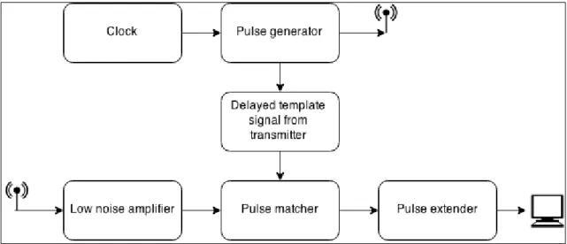
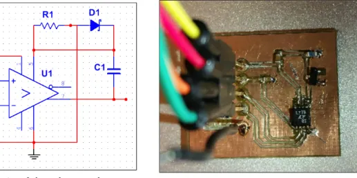
A block diagram of the system can be seen in Figure 1. Here, the method chosen for the functionality of the UWB radar can be observed. The following two sections will describe the implementation of the hardware and the design chosen.
7 Transmitter
An essential part in a UWB is its transmitter. The main task of the transmitter in any UWB system is to generate and send out a short pulse in the order of nanoseconds. This is done with the use of some sort of pulse generator. Also, there is usually a pulse forming step and a transmission line present in the transmitter. In this master thesis, the formed pulse is sent out to the antenna and a delayed pulse is sent to the receiver in order to match the incoming pulse. See Section 4 for more information. This section describes the development of the UWB transmitter and the implementation of its sub-circuits.
7.1 Pulse Generator
During this master thesis a number of different pulse generators were created and tested to evaluate which type would produce the most suitable pulses. Mainly, one pulse generator was made and developed into many versions.
A predominant key component in many low cost pulse generators is a SRD. Due to limited avail-ability of this component, it was not used in this project. A PIN diode in certain conditions is described to have similar characteristics as a SRD when used in a comb generator, which is a common type of pulse generator [52]. PIN diodes are more available than SRD, it was used as a replacement in circuits that required it as a prototype. It was however noted that there might be some limitations in higher frequencies compared to a SRD.
To evaluate if Multisim were able to simulate the effect a PIN diode can preform, it was simulated in Multisim and the same circuit was physically tested in order to compare the outputs. This was done to examine whether it was reasonable to test whole circuit modules by simulation first or if the behaviour was too different for a simulation to be reliable. The outputs from the two circuits are depicted in Figure 2, the circuit was a diode with a load and a sine wave as input. The two signals was deemed to not correlate enough to satisfy that the simulation data would represent an entire module containing a PIN diode good enough. Some circuits does also rely on a physical distance of traces, a so called transmission line, where the distance of a specific track is very important as it decides the pulse width. These circuits were not simulated in Multisim.
This section is divided into two subsections. First, the main pulse generator with its iterations is described and secondly the alternative pulse generators tested are discussed.
7.1.1 Pulse Generator V1.0
The first pulse generator built was based on mainly two reports on UWB pulse generators [53, 54]. This type of pulse generator has been developed throughout the whole master thesis. It was created in three different versions, where each version has a number of patches.
(a) Output behaviour of a PIN diode (b) Output from Multisim simulation of a PIN diode
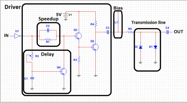
The schematics and main building blocks of the pulse generator can be seen in Figure 3. The purpose of the driver is to create a triggering pulse for the transmission line. The driver contains a speed-up step, a delay step and two transistors for creating the pulse. When the signal from the inverter enters the driver, it will go through the speed-up step as well as through the delay line. The signal from the speed-up will reach the transistor first, opening it up. When the delayed signal reaches the other transistor connected to ground it will short circuit the first transistor, thus ending the pulse. The fall time of the driver output needs to be short enough for the transmission line to be triggered.
The purpose of the transmission line is to convert a fast falling edge from the driver into a narrow pulse. Originally in the design, it contained a SRD. As there is limited availability, it was replaced with a PIN diode. After the driver there is a bias current added to the system. This bias keeps the PIN diode forward biased when no pulse is present. There is also a Schottky diode on the transmission line and it is reverse biased in this state. When a driver pulse reaches the transmission line, the PIN diode will turn off, creating a negative falling edge which goes both directly to the capacitor and output and to the now forward biased Schottky diode. The Schottky diodes short-circuits the system and the inverted signal is reflected back to the output. The unchanged falling edge and the inverted waveform are then summed up to a pulse by the help of a capacitor at the output [54].
Figure 3: Schematics of the main pulse generator and its sub-circuits.
Implementation of pulse generator V1.0
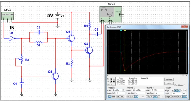
The driver circuit was simulated in Multisim as there were no special components included in this step. The output from the simulated circuit can be seen in Figure 4. The output fall time is at 1 ns and according to the report that the circuit is based on this time should be at 600-700 ps. The simulation result was considered reasonably close enough to the expected value and the circuit was constructed for further testing.
This pulse generator was the first circuit built. At this early stage into the project, the length of cables and tracks were not optimized as the main priority was to get the circuit to work, even if poorly. In order to have the ability to change the length of the transmission line for longer or shorter pulse length, a socket strip was added between the two diodes on the transmission line. A cable of desired length
Figure 4: Schematics and output of the driver in the main pulse generator.
As presented in Section 10.1, the output pulse was not satisfactory. In an attempt to improve the circuit, one by one the components were changed to different values. First, the driver was examined, as the issue seemed to be that the driver pulse fall time was not short enough. To decrease the fall time it was believed that either the transistor or the speed-up step had to be faster. The speed-up was modified by decreasing the capacitor value so that it would de-charge faster and thereby speed up the driver fall time. Different values were tested but no noticeable change was observed. The resistor value in the speed-up was modified, but like the capacitor, it made no major difference to the driver output. In total, the fall time was shortened down by a couple of nanoseconds, from about 15 ns to 10 ns.
The driver transistor was replaced (transistor Q3 in Fig. 3). The transistor MMBT3904 was replaced with a transistor of model BFG135, which should be faster [55, 56]. However, this did not affect the system remarkably. At this point, the output pulse width had decreased from the initial 30 ns to about 20 ns. After soldering off and on components many times, the PCB was worn down and therefore a new PCB was made to clean it up. This new PCB is described in the following section.
7.1.2 Pulse Generator V1.1
In this version the PCB layout was altered. This was done by mainly shortening the PCB tracks and replacing components of the first pulse generator. The overall placement of the components stayed the same. The microstrip line between the Schottky diode and PIN diode was redesigned by removal of the socket strip to reduce the distance between the two diodes. Two vertical lines were added to the PCB so that the physical distance between the diodes could be changed by adding a microstrip over the two lines at a desired distance from the diodes. The design can be seen in Figure 5.
The bottleneck in this circuit appeared to be that the transistors were not fast enough, as the driver fall time was not noticeably affected when manipulating the circuit. The only significant change was introduced ringing, most likely from the self-frequency of the capacitors in the system. The transistor BFG135 (Q3) was replaced with BFG591 [56]. After the replacement no remarkable difference in the output was seen. It was concluded that not enough current was delivered to the transistors, which could be crucial as they are of the type BJT and therefore current controlled. Thus, the inverter 74HCT04
(U1) with an output current of 6.8 mA was exchanged to an inverter of model SN74LVC1G04 with a 32mA output [57, 58]. No significant changes to the output signal after this modification were made. The last capacitor in the driver, just before the bias, was changed in value from 10 nF to 180 pF. See Section 10.1 for the results.
The circuit was further tested in a network analyzer and spectrum analyzer. The network analyzer did not give any results. A test in the spectrum analyzer gave a response which was observed at the received signal from the transmitter as the signal changed along with the generated pulse.
Figure 5: Patched pulse generator V1.1 with a pulse length of 20ns.
7.1.3 Pulse Generator V1.2
In this version of the pulse generator the placement of the components was changed. The circuit became more compact and track lengths were minimized. This was an attempt to decrease the interference from other appliances in the surrounding environment and also to decrease the risk of self-resonance in the system. The circuit is depicted in Figure 8.
The 1k Ω potentiometer was replaced with a 200 Ω potentiometer. This was to obtain a higher accuracy, as it was observed that the potentiometer gave satisfactory results at 0-200 Ω. As the new potentiometer had more turns available than the previous component, it could be more fine-tuned. If the resistance would need to be higher, one can easily add a resistor of suitable size. One could also change the capacitor in series with the potentiometer. However, it seemed more practical to have a high resolution potentiometer for tuning than having to replace the capacitor for a suitable value during testing.
The inductor was replaced from 100 µH to 2 nH in order to see what effect this would have on the system. The Schottky and PIN diodes were replaced with a component containing two PIN diodes in series. The results are presented in Section 10.1.
7.1.4 Miscellaneous Pulse Generators
Some other pulse generators apart from the main one were made. Theses pulse generators are built up differently and uses other technologies to generate pulses. These circuits will be described in the following section.
Figure 6: Pulse generator V1.2.
Tunable Pulse Generator
A tunable pulse generator made can be seen in Figure 7, where Figure 7a shows the circuit built and Figure 7b depicts the corresponding schematics. This version is based on a report about a tunable pulse generator [59]. The idea of this pulse generator is to have transmission lines of different length depending on how wide pulse is desired. It can then be controlled which path to use and thereby determining the pulse width. In this circuit the diode D2 in Figure 7b is originally a SRD, but was replaced with a PIN diode during testing. The other three diodes are PIN diodes as should be according to the schematics.
The functionality of this circuit is that a reversed pulse shuts down the charged SRD which creates a sharp falling edge as the SRD becomes discharged. This falling edge travels through the system directly to the output, creating the start of the pulse, and also through the PIN diode configuration, which acts as a delay step. There is a transmission line between diode D3 and D4 which decides the pulse width. The polarity of the pulse is reversed through the use of a short-circuit and the two components are summed up to create one pulse.
The pulse generator of this type was made with only one transmission line, as the main goal was to examine how well this type worked. This circuit was not simulated as it contained both PIN diodes and a transmission line, which as stated in Section 7.1 was difficult to simulate in Multisim. The pulse generator worked at the first try, however poorly. See Section 10.1 for the results. Increased voltage of the square wave resulted in more ringing of the output. This circuit was not further developed after the first version due to very poor results. It was believed that one of the reasons why the circuit worked poorly was due to the usage of a PIN diode instead of an SRD. Another theory is that it was due to the transmission line being too long. If this was the case, then likely a modified version with shorter delay line would produce a shorter pulse.
(a) Tunable pulse generator circuit. (b) Schematics of the tunable pulse generator.
Figure 7
Comparator based pulse generator
Another pulse generator was created, based upon Williams work presented in ”Simple nanosecond-width pulse generator provides high performance” [60]. The idea behind this version is to have two delayed signals, one with a small offset with respect to the other. This is achieved by a small offset in value of two resistors which are placed in parallel at the start of the circuit. The schematics can be seen in Figure 8. Each signal goes through a comparator and then to an AND gate. The first signal will reach the comparator and produce a low output. Right after, the second signal will reach its comparator and produce a high output. The first signal will then end and switch the comparator to high while the second signal is still high. This opens the AND gate and creates the start of a pulse until the second signal goes back to low again and closes the gate along with the pulse. The input signal to this circuit is a sine wave from the function generator which converts to a square wave through a comparator.
Compared to the results of the main pulse generator V1.2 (Section 10.1), this generator gives out a weaker but about as wide pulse. As the AND gate did not go all the way up to 5 V before switching, it was considered that the limitation was due to a too slow logic gate. This circuit did not perform better or as good as the main pulse generator and therefore it was not further developed.
8 Receiver
One main part of a UWB radar is its receiver. In this master thesis, the receiver is defined as being responsible for collecting a signal through an antenna and match it with the delayed pulse. It then processes the matching data in order to make an assumption of the potential object found. In this section the receiver step, its sub-circuits and design will be discussed. A block diagram of the receiver can be seen in Figure 1.
8.1 Pulse Amplification
After the antenna has received a signal, the signal amplitude will have decreased compared to the original pulse sent out of the transmitter. As the energy level of a UWB pulse is already very low and the received pulse will have lost some of its amplitude, an amplification of the received pulse is necessary. The first step after reaching the antenna is therefore through an LNA. The characteristics of an LNA makes it very suitable for UWB applications. It is very good at amplifying weak signals while keeping the noise level low [61]. However, as an UWB signal is at noise level, it is necessary to collect and add a number of pulses so that the noise cancels out while the signal grows.
There were no simulations made of the LNA circuits tested during this project. The reason for this was because it was assumed that the LNA test circuits which were taken and made from their respective data sheets were correct. Also, as the LNA’s are very sensitive to interference it was thought that a representative simulation would be difficult to achieve.
There were five LNA circuits made during this master thesis. The first LNA [62] version 1 (V1) purchased was about half the price compared to the other LNA:s found, which costed in the range of 60-70 SEK. A suggested circuit from its data sheet was made in order to test the performance of the LNA. However, as mentioned in result 10.1 it did not preform well and after some further testing and modification that was suggested in the data sheet, it was discarded as it was never providing any useful output.
The second LNA used was SPF5189Z, a more expensive version than the first one [63]. The data sheet provided two different configurations, one optimized for 900 MHz and the other for 1900 MHz. The data sheet also provided an evaluation board which was used as a base for the PCB layout. The output of the 900 MHz version is described in result 10.1, it proved to be very unstable and was therefore not used. The second configuration, adapted for 1900 MHz, proved to even more unstable. The PCB layout was redesigned to match the layout of a evaluation board of the 1900 MHz test circuit [63]. After these changes the system became more stable and was not affected by the surroundings as easily. However, the signal response itself did not improve and no amplification was present. The cable lengths and track lengths were shortened down and SMA connectors were added to the output and input of the circuit. This modification made the self-resonance disappear.
Two designs were made for two similar LNA:s, BGA420 and BGA616 [64, 65]. Both were only tested briefly as similar behavior as the previous LNA:s was observed. BGA420 was discarded as it was unstable and BGA616 did not amplify the signal enough. Both used schematics from respective data sheet, but no PCB layout were available. The layout was instead based on a evaluation board SPF5189Z [63].
The final LNA tested in this project was MGA30889, which is of type gain block [66]. The data sheet provided test circuits which the PCB layout was based on. To reduce the risk of issues such as self-resonance, together with SMA connectors for the input and output, the connectors to the supply voltage and ground were also more carefully designed. This LNA circuit gave an usable output which is described in 10.1.
8.2 Pulse matching
After the received signal has been amplified it needs to be matched with the delayed pulse from the transmitter in order to check the similarity and whether a match has been found or not. This step was
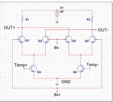
done using a four quadrant Gilbert cell. Two kinds of Gilbert cells were made, a basic version and a more advanced Gilbert cell. Two circuits of each version were implemented and tested.
Gilbert cells are commonly used in IC as a frequency mixer to shift a data signal in or out from an RF signal. This is done with the help of a local oscillator as one of the inputs to the cell but can used as a signal multiplier instead. The four quadrant is able to handle four different input signals and generates two output signals. The inputs are coupled two and two where one dealing with the positive part and one dealing with the negative part of the signal. The negative should be inverted to a representative positive signal to work. The output signal represents a multiplication of the two signals, as it is four quadrant, one of the output represent a negative answer and the other a positive. A Gilbert cell is usually either a linear multiplier or logarithmic but linearization requires additional components over the basic version and are not a necessity in this application[67].
The Gilbert cell needs a template input and an input from the signal to be matched. In this case, the template signal is the delayed pulse from the transmitter and the other input is the received pulse from the antenna. During the testing of the different Gilbert cells, a sine wave from the function generator was used as a test signal. As template, a DC signal was used. When the sine wave matched with the DC level, the output dropped respectively. The more the output level dropped, the better match was obtained. If the DC signal is very low, then the matching level will be very weak and the output will not drop as much as for a higher DC value. It is also important that the signals are high enough, for the transistors to open up properly.
Figure 9: Schematics of a basic Gilbert cell.
8.2.1 Advanced Gilbert Cell
The first Gilbert cell to be built was a multiplier based Gilbert cell being founded on another UWB receiver project [68]. This Gilbert cell, like most Gilbert cells, multiplies currents. Two advantages with this design were the ability to integrate multiple pulses by controlling when the integration should be reset and that the integration converts the current output into voltage output, which is easier to analyze. Both of these additional features are desirable and needs to be implemented in some way or another in the system. The multiple pulse integration is used to increase the certainty of a correctly
This circuit was first simulated in Multisim. However, the simulation did not give expected outputs and also there was an issue in the simulation which resulted in the simulation constantly crashing. It was decided that a circuit should be made despite a non-functional simulation. The reason for this was because it was thought that the circuit could be more easily evaluated and manipulated when having a physical circuit to test. Also, as the behaviour of the advanced Gilbert cell was not fully understood, a physical circuit was considered to help the understanding of the functionality.
The first version used BFG591 Bipolar Junction Transistor (BJT)s [69]. However, with this con-figuration no output was obtained. The circuit seemed to become short-circuited when starting up. If only the supply voltage was applied, then the system worked. However, when sending in the template and input signal, the system drew a high amount of current. Whenever this happened, the system had to be reset. The reset was made by removing a transistor and then solder it back on again. The cause of this behaviour was thought to be either because the capacitors did not discharge or that the kick start effect that should take place in order to start the system did not function.
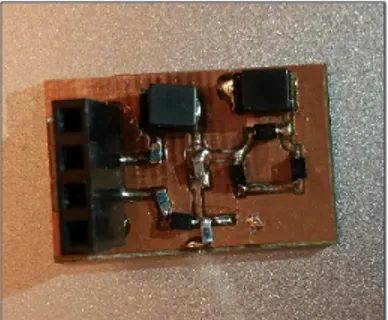
After some research, it was discovered that metal oxide semiconductor field effect transistors (MOS-FET) should be used for this design, which is presented in the paper on a UWB receiver [68]. Therefore, the circuit was modified and produced to be used with MOSFETs instead. This version did not give any expected outcome. The output did not correlate with any kind of multiplication. The circuit acted differently depending on the clock frequency and the inputs did not affect the system as they should. Also, the clock was present in the output signal. The PCB is depicted in Figure 10.
Figure 10: The second version of the advanced Gilbert cell using MOSFET:s.
8.2.2 Basic Gilbert Cell
As the advanced Gilbert cell did not work as expected, it was decided that a more basic Gilbert cell should be built. The main idea of making this version was to achieve a better understanding of how a Gilbert cell works. This would also result in better manipulation of the Gilbert cell in order to add or change functions for it to be tailor-made for the receiver step. For the schematics of the basic Gilbert cell, see Figure 9.
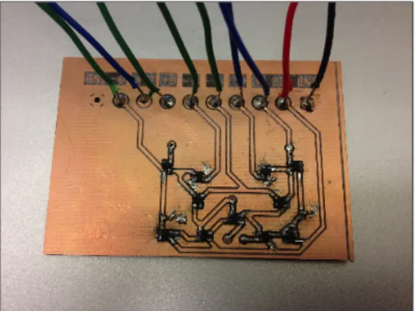
The first version of the Gilbert cell can be seen in Figure 11a. The transistors used for this version were of type MOSFET. This circuit had similar issues as the first advanced Gilbert cell as it was short circuited after start-up. The transistors were examined and it was discovered that they broke easily, presumably because they were not powerful enough. Therefore, another circuit was made using BFG591 BJTs instead [69]. This version worked as expected. A picture of the second version PCB can be seen in Figure 11b. For the results of this circuit, see Section 10.1.
(a) The first version of the basic Gilbert cell using MOS-FET:s.
(b) The second version of the basic Gilbert cell using BJTs.
Figure 11: The two basic Gilbert cell circuits.
8.3 Pulse Extender
After the two pulses have been multiplied, the data is to be sampled and processed in order to draw a conclusion of the detected object in question. This step is very critical when designing a low-cost system, as the simple solution is to use a fast ADC in the order of about 20 Gigasample per second (Gsps). As fast ADCs are very expensive, this is not a reasonable solution for the goal of this master thesis. The need for such a fast ADC is to oversample the pulse enough for retrieving a satisfactory representation of the appearance of the nanosecond short pulses. In order to remove the need for a fast ADC, the pulse is sampled and extended. The method used for this project is based on holding the pulse before sampling it to the software. The idea is to hold the nanosecond pulses for about a microsecond. This would decrease the sampling speed, thus allowing for a slower, less expensive, sampler to be used. The circuit is based on a pulse stretcher [70]. The schematics is shown in Figure 12a.
This circuit also has an adjustable object detector function built into it. This part is built up of a Schmitt trigger and a digital resistor. Tuning of the resistor changes the threshold for the object size to be detected. The purpose is to have the ability to change the threshold for the energy level from the pulse matching at the Gilbert cell. This allows for detection of objects of desired size. When the threshold has been reached, the sample and hold function will trigger, elongating the pulse.
For the development phase, the digital resistor was replaced with a potentiometer in order to test the circuit without software. After some modifications, this circuit worked as expected. Depending on the value of the resistor the delay increases or decreases, where higher values increase the delay time. The results are presented in Section 10.1.
(a) Schematics of the pulse extender. (b) Pulse extender circuit.
Figure 12: Pulse extender.
9 EMC
As soon as high speed digital or high frequency analog electronics is designed, electromagnetic compat-ibility (EMC) has to be taken into consideration with great care. Electromagnetic interference (EMI) is a core part of EMC as it describes the phenomenon of disturbance while EMC is how to control it. EMC is not excluded to high frequency electronics but it is much more prevalent in that field. Each part in a circuit is susceptible to the problems that can occur including self-resonance, loss of power, interference emittance and interference susceptibility. The received interference is commonly picked up in the system with cables, long traces or from the power source. As a radar system often deal with weak signals, the introduced noise can be as strong as the signal itself if it is introduced in the wrong place. Similarly, fast internal switching can leak out radiation via cables or long tracers and if the circuit is not properly shielded [71].
Impedance matching is also a very common issue when it comes to wireless technology, often when dealing with an antenna. Matching impedance will allow for a better transfer of power between two nodes, for example between an signal amplifier and an antenna. The power that is not transferred can bounce back into the circuit which can create standing waves or worse, damage some sensitive components. Radar and other wireless technology often use 50 Ω as the default impedance. Using one of the standard impedances make it easier to buy components or connectors that are matching. The ideal scenario is when the impedance between two stages is 50 Ω without any inductance or capacitance over the entire frequency range, which is very hard to achieve [72]. Capacitors and inductors changes their behavior with changing frequency and can even swap behavior, an inductor can act as a capacitor and vise versa. This is due to the parasitic properties of real life components. The characteristics of the impedance can be measured with a network analyzer where the most common parameter is the S parameter. The S parameter describes how much power is lost at specific frequency and the response impedance, giving the complex impedance where the imaginary part describes the capacitance or inductance. Impedance matching is often achieved with small circuits called L-networks or Π-network, transformers or with a tunable IC. Some ICs can even automatically tune, detecting signal bounces and altering the impedance accordingly to get the maximal power transfer. However most matching techniques are matching for just a few frequencies or are only applicable on lower frequency which makes it hard to match for such a wide band in which UWB operates in [73].
All these problems are no less of a problem when dealing with UWB radar where high frequency signal is present. As the wavelength of a GHz signal, where UWB often operate, is close to the size of a PCB, the trace design is important. Controlling the trace length can reduce the risk of generating
standing waves within the circuit or absorbing signals of specific frequencies. Many types of pulse generators do also contain closed loops, adding a risk of self-resonance with capacitors. A typical source of EMI comes from IC:s anda way of dealing with it is by having decoupling capacitors as close as possible to the supply pin.
9.1 EMC Issues in this project
This project started off with little consideration about EMI, as the initial goal was to get the circuits to just work before improving and matching the circuits. The idea was to speed up the process of evaluating different circuits. The first instance where it became an obvious issue were with the very sensitive LNAs. The initial thought was that the LNA circuit would work, even if poorly, but were proven not to give any proper response. Issues that arose with the LNAs were self-resonance, ringing signals and flat out dead signals. To solve these issues, new PCB designs were made where the trace length, component placement, cable length and connectors where more carefully considered on the different LNA circuits. When all those problems were reduced, the act of using an oscilloscope probe proved to be enough to disturb the system enough to generate self-resonance. To solve this, SMA connectors were used on key points to connect to the oscilloscope directly with SMA coaxial cables, keeping the impedance at 50 Ω. In figure 13, one of the improvement on one LNA can be seen. This is the difference that shortening the cables made, from just creating a self-resonance signal to an impulse response.
The probes used for measuring circuit signals on the rest of the system had to be re-evaluated as it was discovered that they caused self-resonance in the system. This lead to small modifications of adding SMA connectors to some of the existing circuits, including pulse generators, to be able to better see a more representative signal in the oscilloscope as they also deal with the high frequency signals. The circuits are not as affected with an oscilloscope probe everywhere, but it is generally good to make sure how the probes affects the system. Also, if possible using a probe with a high multiplier is preferable to lessen the load on the device under testing (DUT).
The impedance matching has been one of the last steps to be considered, as it will be affected by any component changes close to the matching. The primary focus of the impedance matching is around the antennas, to be able to send and receive as good signal as possible. There exists equations to estimate impedances and how to match it, but they can quickly become a highly non-linear, multivariate system even in basic cases. The approach was to solve it through empirical research with different networks, aiming to match for a center frequency while trying to minimize the mismatch for the rest. However due to time limitation, the impedance matching was not finished in the final circuit design and just contains an inverted Π-network to the antenna.
10 Results
In this section the results of the master thesis will be discussed. The results will be based on the problem formulation questions as to give a representation of how well answered these questions are.
10.1 Q1: What are the drawbacks of a low cost UWB radar?
As discussed in Q1 (2), many aspects of designing an UWB were time consuming and different circuits showed a big variation in performance. Most of the circuits were built from primary basic components such as diodes, transistors, resistors, inductors and capacitors. Most of the duration during this project was spent on researching, building and evaluating different UWB modules. An IC module usually comes with a datasheet complete with information on how to balance the circuitry around it, requiring less time spent on repetitious work regarding filtering and component compatibility.
The following modules have mostly just been tested separately and the behavior described here was in that single module configuration. The components that is dealing the high frequency signal are limited to 2.6 GHz as it is the maximum operating frequency for some of the components in the system. Each circuit lacks the proper support components like power regulators, polarity protection, clocks, shielding, spike protection and other common safety circuitry. All the different supply voltages were provided by a power cube. Similarly, all the clocks or input pulses were made using a function generator.
Main Pulse Generator
The first module to be built was the pulse generator, the key component of most low cost alterna-tives used a step recovery diode (SRD). SRD:s are however not widely available so the component was replaced with the more common PIN diode, which shares some of the properties used for pulse generation [52]. None of the pulse generators that were built could achieve the same short pulse width as what was reported in the articles which the circuit designs were based on. The first Printed Circuit Board (PCB) made of pulse generator V1.0 (Section 7.1.1) gave a very weak pulse, at about 100 mV, with a pulse length of 25 to 30 ns. With some minor tweaking on the circuits the pulse width was shortened down to 20 ns. The input to the system is the clock, supply voltages and a bias voltage. For this version, a bias voltage of 0.7 V gave a stable Gaussian pulse.
In pulse generator V1.1 a decrease in fall time from the transistors, from 20 ns to 14 ns, throughout the system was obtained. The output pulse was between 15 ns and 25 ns wide depending on the value the potentiometer, although a change in bias voltage to 0.8V resulted in a 10 ns wide pulse. The output peak voltage of the pulse was increased to 1.5 V.
The output from the driver of Main Pulse Generator V1.2 (see Section 7.1.3) was improved com-pared to the previous versions, with a fall time of 10 ns. The output could be reduced to a 8-10 ns wide pulse with carefully tuned potentiometer value. The peak voltage dropped down to 1 V. A slightly wider pulse output pulse can be seen in Figure 14. The main pulse generator showed inconsistency in the pulse strength between pulses, which was apparent in all of the versions. The final version contained the widest frequency spectrum (figure 17a). The final version was tested in the network analyzer and from Figure 17b, it can be observed that the trace follows the 50 Ω resistance circle. The trace lies within the inductive area, so if the circuit would be made more conductive the trace would naturally stabilize around 50 Ω.
The frequency response characteristics of the pulse generators varied greatly, even between different versions of the same base design. All generators had a low minimum frequency close to 1 KHz but the maximum frequency ranged from 100 MHz to around 2.5 GHz. The pulse generator that was chosen to be used is described in the section 7.1.3.
Tunable Pulse Generator
The tunable pulse generator in section 7.1.4 gave the widest pulses out of the three generators. The output gave 100 ns long pulses with a peak voltage of 200 mV. The input to this system was a 6 V peak
Figure 14: Output pulse from pulse generator V1.2
to peak square wave and a supply voltage of 0.6 V. Increasing the supply voltage gave an increased peak vale but also added some ringing. The output can be seen in figure 15.
Figure 15: Output pulse of tunable pulse generator with a pulse length of 100 ns.
Comparator based Pulse Generator
The comparator based pulse generator in section 7.1.4 (figure 15) outputted pulses ranging from 20 ns to 40 ns with an amplitude of 300 mV. The input to this generator requires only supply the IC:s and an input clock. A generated pulse from the comparator based pulse generator is depicted in Figure 16.
Gilbert cell
The second module was the pulse comparator, where the designs are based on a four quadrant Gilbert cell multiplier. Two different designs were made. A more complex cell was made which had more functionality in the design. It allowed the output current to be converted into output voltage via integration and it also supported resetting of the integration, allowing multiple pulses to be integrated in the Gilbert itself [68]. Two different version of this circuit were made, only differentiating with
Figure 16: An output pulse from the comparator based pulse generator.
worked as intended, they showed no output response with varying inputs including DC, sine waves and pulses. The second design was based on a basic four quadrant Gilbert cell which does nothing else but act as a multiplier. This was also made into two versions, one with MOSFET and one with BJT. The transistors of MOSFET version was destroyed under testing. The version with BJT proved to be more robust. The simplified design worked as intended but lacks the functionality of the more advanced version. Part of the analog analysis is in the pulse matcher. The dropping output voltage correlates to the simultaneous high voltages of the inputs. The inputs to the basic Gilbert cell were a DC signal at 1 V and an AC signal, as described in Section 8.2. The Gilbert cell showed a much greater sensitivity when an offset of 650 mV was applied to the input signals. The output from this circuit can be seen in Figure 18. Here, the maximum value means the smallest match. The lower the value, the higher the match. Lowering the DC input reduced the voltage drop in the output. At the lowest point the multiplication of the two signals gives the highest match. This still gives a short pulse as an output which can be even shorter than the initial pulse. The chosen Gilbert cell is described in the section 8.2.2.
Pulse Extender
The short output pulse from the Gilbert cell is the input to the pulse extender. It provided two function, the first one was to extend a few nanosecond pulse to around a microsecond and the other functionality was the ability to change the trigger level out from the Gilbert cell. The pulse extender is a modified Schmitt trigger with a latch function. The extended pulse length is based on a capacitance and a bleed resistor, where increasing the value of the resistor makes the pulse longer. However, if the pulse is too long, it will interfere with the next pulse. The test input to the pulse extender was a pulse generated from the function generator, with a pulse width of 15 ns. The output from the system is depicted in Figure 19. As the output triggers high and stays high until a given threshold and then turns low, the curve looks very similar to a PWM square wave. It can be observed that the 15 ns input pulse has extended to about 4.3 µs. More detail on the pulse extender can be read in the section 8.3.
LNA
The last required module was the amplifier on the receiver, which is a LNA connected with an antenna. This type of amplifier is very sensitive to incorrect component matching and to the PCB layout. This lead to the making of a total of five different LNA circuits, each with different LNA. The first LNA
(a) The output from the spectrum analyzer. (b) The impedance matching in the network analyzer
Figure 17: Results of the pulse generator in the complete circuit.
Figure 18: Output from the basic Gilbert cell with a DC signal as template input and AC signal as matching input.
circuit was built based on circuit design provided by the manufacturer [62]. With different pulses as an input, there were no amplification of the input signal, but rather a de-amplification. The output signal of the LNA acted very poorly and did not seem correlate directly with the input signal. The circuit was modified by adding a capacitor between the LNA ground pin and ground, for the DC to be blocked instead of going directly to ground. However, no noticeable change was observed. It was believed that due to the low cost of the the LNA, it was more difficult to get it to work as more components for the test circuit was needed than for a more expensive LNA. The EMC was not particularly considered in this circuit.
Two slightly different configurations of the second LNA was tested. One optimized for 900 MHz, the initial circuit generated very unstable peaks from an input pulse and was very prone to self-resonance. The test circuit was modified into another very similar test circuit optimized for 1900 MHz by replacing values of some capacitors and removing an inductor. However, this version generated an even more unstable outputs than the previous circuit configuration and both sine waves and pulses as input often created self-resonance of higher frequency. The final design used proper SMA connectors for input and output, this eliminated the issue with self-resonance but did not provide an amplified signal and the output signal did not follow the shape of the input. This was true for both a sine wave and a pulse as
Figure 19: Output from the pulse extender.
Two similar LNA:s were used, BGA420 and BGA616 for the third and forth circuits [64, 65]. BGA420 provided no output response for input pulses and outputted mostly noise when with a sine wave was used as an input. The circuit with BGA616 showed a proper correlation between input and output from the LNA and were not prone to self-resonance but with a negative gain of 1.
A circuit based on the LNA MGA30889 were made, It proved to be both stable, resilient to self-resonance and provide a negative gain of 6. The signal had some slight ringing after passing the amplifier. The output signal from the LNA is depicted in Figure 20, where a 15 ns wide Gaussian pulse was used as input and the LNA had a supply voltage of 4.8 V. A common output from the unstable LNA’s is depicted in Figure 21.
Figure 20: An amplified output from an stable LNA circuit.
10.2 Q2: Will the bottleneck be in software or hardware?
In Q2 (2), the location of the bottleneck is discussed, whether it will be in software or hardware. As the software was not developed during this thesis due to time constraints, this question cannot be answered as of now.
Figure 21: Output from an unstable LNA test circuit.
The hardware contains several bottlenecks which are related to the delay signal, relative long pulse width and the down conversion of the received signal. A pulse width of 10 ns gives a very low precision as it would make it challenging to distinguish between two objects 1.5 m apart according to equation 1. The delayed template pulse limits the physical distance between the transmitter and receiver as the signal contains high frequency components. The longer the signal travels, the more of the microwave frequencies are lost resulting in a distorted signal as a template. Longer distances makes it also more susceptible to external noise being absorbed. The lowest limit on the components in the circuits is not rated for frequencies greater than 2.6 GHz. This prevents the system take advantage of an improved pulse generator which can generate signals with higher frequency components.
The system is designed to only trigger to a received signal together with the delayed signal which is tied to a specific distance. But as the signal is so long, the end part of a pulse can be enough to match the beginning of the expected pulse giving a match for a closer object. For the same reason, the minimum detection range with this pulse width is 1.5 m. The down conversion introduces two limitations, it limits the pulse repetition time as two pulses will overlap if the extended pulse is longer than the time between two pulses. The second limitation with the pulse extender is the loss of information. The pulse matcher produces an output signal depending on how well the received signal matches with the template signal, giving an indication on how the signal has been altered. Most of that information is lost in the pulse extender as it only acts like a peak detection.