,
STOCKHOLM SWEDEN 2020
Error Injection Study for a
SpaceFibre In-Orbit
Demonstrator
CARLOS ABAD GARCÍA
KTH ROYAL INSTITUTE OF TECHNOLOGY
SpaceFibre In-Orbit Demonstrator
Master Thesis
Carlos Abad Garc´ıa
Examiner: Johnny ¨
Oberg
University Supervisor: Kalle Ngo
Company Supervisor: Manuel S´
anchez Renedo
A thesis presented for the degree of
Master of Science in ICT Innovation - Embedded Systems
Electronics and Embedded Systems - KTH Royal Institute of Technology
Digital Electronics Group - Thales Alenia Space Espa˜
na
Demonstrator
Master Thesis - KTH Royal Institute of Technology
Carlos Abad Garc´ıa
Abstract
The space electronics sector is shifting towards the New-Space paradigm, in which tradi-tional space-qualified and expensive components and payloads are replaced by commercial off-the-shelf (COTS) alternatives. This change in mentality is accompanied by the de-velopment of inexpensive cubesats, lowering the entry barrie in terms of cost, enabling an increase in scientific research in space. However, also well-established and resourceful spacecraft manufacturers are adopting this trend that allows them to become more com-petitive in the market.
Following this trend, Thales Alenia Space is developing R&D activities using COTS com-ponents. One example is the SpaceFibre In-Orbit Demonstrator, a digital board inte-grated in a cubesat payload that aims to test two Intellectual Property blocks implement-ing the new ECSS standard for high-speed onboard communication.
This thesis presents the necessary steps that were taken to integrate the firmware for the demonstrator’s Field-Programmable Gate Array (FPGA) that constitutes the main pro-cessing and control unit for the board. The activity is centered around the development of a Leon3 System-on-Chip in VHDL used to manage the components in the board and test the SpaceFibre technology.
Moreover, it also addresses the main problem of using COTS components in the space environment: their sensitivity to radiation, that, for a FPGA results in Single-Event Up-sets causing the implementation to malfunction, and a potential failure of the mission if they are not addressed. To accomplish the task, a SEU-emulation methodology based in partial reconfiguration and integrating the state of the art techniques is elaborated and applied to test the reliability of the SpaceFibre technology.
Finally, results show that the mean time between failures of the SpaceFibre Intellectual Property Block using a COTS FPGA is of 170 days for Low Earth Orbit (LEO) and 2278 days for Geostationary Orbit (GEO) if configuration memory scrubbing is included in the design, enabling its usage in short LEO missions for data transmission. Moreover, tailored mitigation techniques based on the information gathered from applying the pro-posed methodology are presented to improve the figures.
Demonstrator
Master Thesis - KTH Royal Institute of Technology
Carlos Abad Garc´ıa
Sammanfattning
Rymdsektorn b¨orjar luta mot “the New-Space paradigm”, i vilken traditionella och dyra rymd-kvalificerade komponenter och laster b¨orjar bytas ut kommerciella-fr˚an-hyllan (eng. Commercial-off-the-Shelf - COTS) alternativ. Denna f¨or¨andring i mentalitet ackompan-jeras av utvecklingen av billiga CubeSats som s¨anker entr´e-kostnaden f¨or vetenskaplig forskning i rymden. Aven v¨¨ aletablerade och resursstarka rymdfarkost-tillverkare har anammat denna trend vilket l˚ater dem bli mer konkurrenskraftiga p˚a marknaden.
F¨or att f¨olja trenden s˚a utf¨or Thales Alenia Space R&D utecklingsaktiviteter med COTS komponenter. Ett exempel ¨ar SpaceFibre In-Orbit Demonstrator, a digitalt kort integr-erat i en CubeSat payload som ¨amnar testa tv˚a s.k. Intellectual Property (IP) konstruk-tioner som implementerar den nya ECSS standarde f¨or h¨og-hastighets kommunikation ombord.
Denna avhandling presenterar de n¨odv¨andiga stegen f¨or att integrera firmware f¨or demon-stratorns programmerbara FPGA-krets (eng. Field-Programmable Gate Array - FPGA) som fungerar som kortets huvudsakliga ber¨aknings- och styrenheten. Aktiviteten ¨ar cen-trerad kring utvecklingen av ett Leon3 System-on-Chip i VHDL f¨or att hantera och man-agera komponenterna p˚a kortet och testa SpaceFibre-teknologin.
Vidare adresserar den ocks˚a huvudproblemet med att anv¨anda COTS-komponenter i rymdmilj¨o: deras k¨anslighet f¨or str˚alning, vilket i en FPGA kan resultera i s.k. Single-Event-Upsets, vilket orsakar fel i implementeringen och ett potentiellt misslyckande av uppdraget om de inte adresseras. F¨or att ˚astadkomma detta, utarbetas och appliceras en SEU-emuleringsmetodik baserad p˚a partiell rekonfigurering f¨or att testa tillf¨orlitligheten hos SpaceFibre-tekniken.
Slutligen visar resultaten att den genomsnittliga tiden mellan fel (eng. Mean-Time Be-tween Failure - MTBF) f¨or SpaceFibre IP blocken i en COTS FPGA ¨ar 170 dagar f¨or l˚ag omloppsbana och 2278 dagar f¨or Geostation¨ar omloppsbana om scrubbing-tekniker imple-menteras. Skr¨addarsydda mitigations-tekniker, baserade p˚a den insamlade informationen av till¨ampningen av den f¨oreslagna metoden, f¨oresl˚as f¨or att f¨orb¨attra siffrorna.
I would like to thank my family and friends for staying close and their support, my col-leagues at Thales Alenia Space in Spain, especially Manu, for their help, Johnny ¨Oberg and Kalle Ngo from KTH for the opportunity to carry out this work, and all my friends from Stockholm and Berlin for the great times we had. Thank you.
1 Introduction 1
1.1 Motivation . . . 2
1.2 Purpose and goals . . . 3
1.3 Research Questions . . . 3
1.4 Research Methodology . . . 3
2 Background 5 2.1 AMBA bus, GRLIB and LEON3 . . . 5
2.1.1 AMBA bus . . . 5
2.1.2 LEON3 . . . 6
2.1.3 GRLIB . . . 6
2.1.4 Additional tools . . . 7
2.2 Radiation upsets on SRAM-based FPGAs . . . 7
2.2.1 FPGA technologies . . . 8
2.2.2 KU060 FPGA structure . . . 9
2.2.3 FPGA configuration . . . 9
2.2.4 Upset classification and occurrence . . . 12
2.2.5 Radiation campaigns . . . 14
2.2.6 Upset occurrence for the KU060 FPGA . . . 15
2.2.7 Previous work in SEU injection . . . 17
2.3 Space Fibre . . . 20
2.3.1 Gigabit serial transceivers . . . 20
2.3.2 Space Fibre modules . . . 21
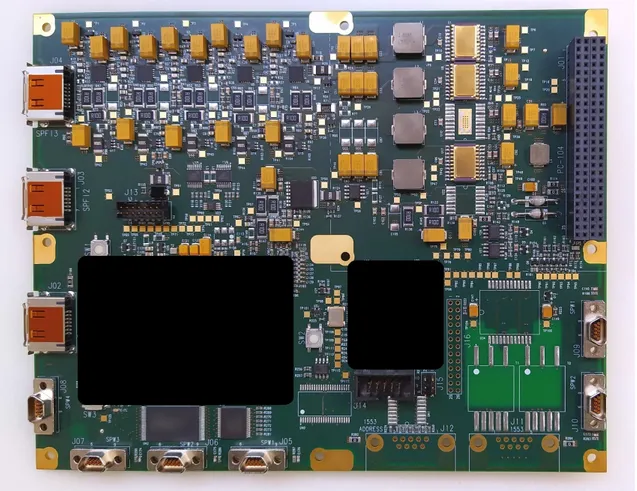
3 Firmware development for the flight demonstrator 23 3.1 Board features and baseline . . . 23
3.2 Developments carried out . . . 24
3.2.1 DSU validation . . . 26
3.2.2 Memory controllers validation . . . 26
3.2.3 SPI controller and multiplexing validation . . . 27
3.2.4 SerDes transceivers validation . . . 27
3.2.5 ESA SpaceFibre IP integration and validation . . . 27
3.2.6 STAR-Dundee SpaceFibre IP integration and validation . . . 28
3.2.7 Final validation . . . 28
4 SEU injection in the SpaceFibre IP core 29 4.1 Design choices . . . 29
4.1.1 Limitations . . . 30
4.2 Architecture of the injection experiment . . . 31 v
4.2.3 Test controller . . . 32
4.2.4 Injector . . . 33
4.3 Testing framework . . . 33
4.3.1 Addresses for the injections . . . 33
4.3.2 Time between each injection . . . 37
4.4 Software architecture . . . 38
4.4.1 Software FSM . . . 38
4.4.2 Serial Communication . . . 41
4.5 Evaluated parameters . . . 41
4.5.1 Severity of the failures . . . 41
4.5.2 Application layer . . . 42
4.5.3 Virtual channel layer . . . 43
4.5.4 Retry layer . . . 43
4.5.5 Lane layer . . . 43
5 Results and discussion 45 5.1 Implementation results in the KU060 . . . 45
5.2 Results for the lane layer . . . 46
5.2.1 Statistical validation . . . 46
5.2.2 Other results . . . 48
5.2.3 Discussion of the results for the lane layer . . . 48
5.3 Results for the retry layer . . . 49
5.3.1 Other results . . . 50
5.3.2 Discussion . . . 50
5.4 Results for the virtual channel layer . . . 51
5.4.1 Other results . . . 51
5.4.2 Discussion of the results . . . 52
5.5 Results for the interface layer . . . 53
5.5.1 Other results . . . 53
5.5.2 Discussion of the results . . . 53
5.6 Results for the broadcast layer . . . 54
5.7 Results for the SpaceFibre IP core . . . 55
5.7.1 Vulnerability factor . . . 55
5.7.2 Discussion . . . 55
5.8 Special events and limitations when using the SEM IP . . . 57
5.8.1 ECC bits . . . 57
5.8.2 Uncorrectable errors . . . 58
5.8.3 Two errors caused by a single injection . . . 59
5.9 Reliability of the SpaceFibre IP . . . 59
6 Conclusion 62 6.1 Contributions . . . 64
6.2 Future work . . . 64
2.1 AMBA bus master and slave multiplexing [1] . . . 6
2.2 Two CLBs and one routing switchbox of the KU060 FPGA . . . 9
2.3 Device view of the KU060 showing clock regions and columns within . . . 10
2.4 Types of Single-Event Effects. [2] p. 4 . . . 13
2.5 SpaceFibre Protocol Stack. [3] p. 36 . . . 22
3.1 SpaceFibre In-Orbit Demonstrator board . . . 24
3.2 developed SoC . . . 25
4.1 Hardware Architecture for the injection experiments . . . 31
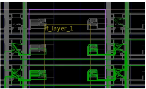
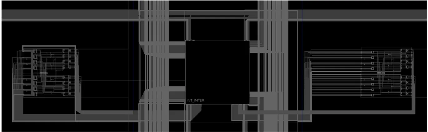
4.2 Pblocks drawn inside a clock region . . . 35
4.3 Pblocks that contains the broadcast layer, in columns 2 to 6 . . . 36
4.4 Interconnect and CLB columns in the interface layer . . . 36
4.5 Software Architecture for the injection methodology . . . 39
2.1 Physical frame address format . . . 11
2.2 Linear address format in the KU060 device . . . 11
2.3 In-Orbit SEU rate for CREME96 [4] . . . 16
4.1 Linear address format for an injection using the SEM IP in the KU060 device 40 5.1 Resource utilization in the KU060 FPGA for each layer of the SpaceFibre IP Port . . . 45
5.2 Parameter measurements for 10 injections in the Lane Layer and its aver-age, standard deviation and confidence interval . . . 47
5.3 Amount of critical bits distributed by severity for the lane layer . . . 48
5.4 Parameter measurements for the injections in the retry layer . . . 50
5.5 Amount of critical bits distributed by severity for the retry layer . . . 51
5.6 Parameter measurements for the injections in the virtual channel layer . . 52
5.7 Amount of critical bits distributed by severity for the virtual channel layer 53 5.8 Parameter measurements for the injections in the interface layer . . . 54
5.9 Amount of critical bits distributed by severity for the interface layer . . . . 55
5.10 Amount of critical bits divided by severity for the broadcast layer . . . 55
5.11 Parameter measurements for the injections in the SpaceFibre IP . . . 56
5.12 Amount of critical bits divided by severity for the SpaceFibre IP . . . 57
List of Acronyms and Abbreviations
This document requires readers to be familiar with the following terms and abbreviations. FPGA Field Programmable Gate Array
IOD In Orbit Demonstrator
RISC Reduced Instruction Set Computer
AMBA Advanced Microcontroller Bus Architecture
SoC System on Chip
GPL General Public License
DMIPS Dhrystone Million Instructions per Second CFI Common Flash Memory Interface
SRAM Static Random Access Memory
RAM Random Access Memory
CMOS Complementary Meta-Oxide-Semiconductor DSP Digital Signal Processing
CLB Configurable Logic Block
LUT Look-up Table
SerDes Serializer-Deserializer LET Linear Energy Transfer TID Total Ionizing Dose SEE Single Event Effect SEL Single Event Latch-up SEB Single Event Burnout SEGR Single Event Gate Rupture
SEU Single Event Upset
SBU Single Bit Upset
MBU Multi Bit Upset
SECDEC Single Error Correction Double Error Code ECC Error-Correcting Code
SEM Soft Error Mitigation
BER Bit Error Rate
CRAM Configuration Memory RAM
DUT Device Under Test
FSM Finite State Machine
PC Personal Computer
FMC FPGA Mezzanine Card
CRC Cyclic Redundancy Check QoS Quality of Service
DVF Design Vulnerability Factor
CI Confidence Interval
CIR Relative Confidence Interval MTBF Mean Time Between Failures
ASIC Application-Specific Integrated Circuit COTS Commercial off-the-shelf
IP Intellectual propery
AXI Advanced eXtensible Interface AHB AMBA High-performance Bus APB Advanced Peripheral Bus GPL GNU General Public License HDL Hardware Description Language DPR Dynamic Partial Reconfiguration BRAM Block Random Access Memory SET Single-Event Transient
Introduction
Nowadays, the space sector plays a major role in scientific experiments, with ambitious observation programmes that monitor not only land and sea, but also integrate complex instruments such as multispectral cameras and synthetic aperture radars, or even more complex sensors that allow to gather valuable information about our environment. A good example is that less than one year ago, in Sevilla (Spain), the European Space Agency (ESA) comitted to the biggest ever budget to be spent in missions to come, that will allow to improve the understanding of both our planet and the universe.
From the engineering point of view, assembling these missions is not only an extraordinary effort, which requires a collective endeavor by multiple teams around the world, but also poses the challenge of developing the necessary technologies. Apart from the instruments themselves, the elements surrounding them also play a key role in these missions. High performance processing and communications onboard the payloads are necessary, since “raw” instrument data is usually too heavy to be sent back to earth directly. There are two key technologies that allow to overcome this challenge:
• Field-Programmable Gate Arrays: FPGAs are programmable integrated cir-cuits that allow to create almost any digital circuit by using Lookup Tables (LUTs) that implement logic functions and programmable interconnections. They offer a processing performance to power consumption ratio of about one to two orders of magnitude higher than processors, and, even though they are not as efficient or powerful as application-specific integrated circuits (ASICs), FPGAs do not incur in the extremely high non-recurrent engineering costs derived from the verification and fabrication of an ASIC. For that reason, FPGAs are usually the chosen platform when high computing power is required and not a significant amount of units will be manufactured. Along the years, several radiation-hardened FPGAs specific for the space environment have been developed. However, they are either less performant than their non radiation-hardened counterparts—due to containing less logic, since a significant part of the silicon is used to protect the functioning transistors—or significantly more expensive. That is why, with the “new-space” paradigm, com-mercial off-the-shelf (COTS) components are starting to be used in shorter less critical. The protection to the space environment is no longer provided by the com-ponents themselves, but by additional conceptual layers of protection implemented at both system level and within the processing elements. This paradigm has not reached to the most critical scientific missions yet, but it is a matter of time, with the performance gap between COTS and space-qualified components, as well as the
biggest FPGA manufacturer—Xilinx—using a COTS non-hardened FPGA as their latest space-grade FPGA: the RT Kintex Ultrascale, which is essentially a Kintex Ultrascale KU060 with a ceramic flatpack packaging.
• High-speed onboard communications: with the huge data rate created by the aforementioned instruments, as well as the processing rate of the multiple computa-tion units and storage elements, the need for board-to-board communicacomputa-tion able to transfer data at gigabits per second is a common requirement in different space mis-sions. This demand is partially covered by the latest high-speed serial transceiver technologies, that use serializer-deserializer circuits—sometimes several of them in parallel lanes—allowing to achieve the demanded speed. However, there was no network standard designed for its usage in space until the recent development of SpaceFibre, which integrates a network architecture specifically designed for space, and with the same application interface as SpaceWire—a current standard for on-board communications at lower speeds supported by ESA, NASA and JAXA among others. SpaceFibre provides Quality of Service (QoS) mechanisms over the physical layer, allowing for flow-control and error recovery and management among other more sophisticated capabilities at an extremely high data-rate. The standard was published in May 2019, by the University of Dundee under ESA funding, and some Intellectual Property (IP) blocks that implement the protocol have been developed already.
1.1
Motivation
This work is framed in a collaboration between Thales Alenia Space Spain and a commer-cial space company motivated by these two factors. The aim of the project is the develop-ment of an experidevelop-mental digital card, the SpaceFibre In-Orbit Demonstrator (IOD) that integrates a current generation COTS FPGA based on Static Random-Access Memory (SRAM), the kind that is expected to be adopted in the space sector. The FPGA contains two SpaceFibre IPs developed by Cobham Gaisler/ESA and STAR-Dundee integrated in a System-on-Chip (SoC) based on the LEON processor that manages all the elements in the board needed to test and validate the SpaceFibre technology as well as the FPGA. All stakeholders involved have great interest into testing and accumulating hours of flight into the different components, constituting a relevant research and development activity. Apart from testing the components in-flight with the demonstrator, with the new-space paradigm and the shift to COTS components, it is of capital relevance to characterize their behavior when subject to radiation before flight, in accelerated campaigns that emulate the effects of the space environment and allow to gather data expected for the mission. For particular components, this is done by performing costly accelerated radiation campaigns, in which a device is exposed to a controlled radiation source, while being monitored for failures. However, as latest campaigns show, for FPGAs, there is a noticeable difference on the failure rates depending on the architecture of the circuit subject to radiation. Apart from the countless implementations that an FPGA allows due to its programmable nature, the need to test the mitigation techniques used for a particular mission make the usage of radiation campaigns impractical, since one separate campaign for each of them would be necessary.
Hence, a research effort is being carried out to emulate the effects of radiation by injecting SEUs in the device to substitute radiation campaigns. It is a relatively new field, and still has not been applied as a validation step in a real implementation, but its poten-tial in saving costs is immense, and valuable contribution can be made by designing a methodology that gathers the state-of-the art techniques and applying it to a relevant implementation.
1.2
Purpose and goals
There are several goals to be achieved for this work:
1. Development of the firmware for the SpaceFibre IOD implemented in the demon-strator board integrating both IPs with the LEON3 SoC and high-speed transceivers 2. Validation of the firmware and support for the integration of the application software
in charge of running the recursive tests for the different components
3. Performance of a literature review of the state of the art in SEU emulation
4. Development of a state of the art framework and methodology for SEU emulation. A key step for achieving this goal is to locate a particular design within the FPGA configuration memory
5. Application of the developed methodology to the SpaceFibre IP to obtain results, interpret them and obtain reliability metrics as well as propose recommendations to reduce its SEU vulnerability
The purpose is to contribute to the creation of the SpaceFibre IOD with COTS compo-nents, as well as to show the effectiveness of SEU emulation by creating and applying a state of the art injection techniques to the SpaceFibre IP, which will also contribute to the development of the SpaceFibre technology itself and the adoption of COTS components in the space sector.
1.3
Research Questions
The aim then, is to answer to the following research questions: • How to integrate the SpaceFibre technology in a LEON3 SoC?
• Is the combination of SpaceFibre with a COTS FPGA ready for a commercial mission?
1.4
Research Methodology
To answer these questions, this project follows an inductive approach to carry out the firmware and integrate it into the demonstrator board as well as for the development of the injection methodology. Both elements were carefully designed from the theoretical grounds and calculations, following a qualitative research methodology [5]. However, the
second part of the project, that constitutes the injection campaign and interpretation of the results is inherently experimental and deductive. For this part, the designed method-ology is applied in different experiments, collecting a large dataset and interpreting the results from the statistical point of view, using a quantitative methodology.
Background
This chapter introduces the previous research and literature that are the foundations of this work, as well as the necessary concepts to understand it.
2.1
AMBA bus, GRLIB and LEON3
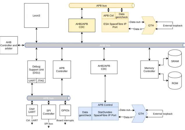
One of the main contributions from this thesis is the implementation of the firmware used for the SpaceFibre IOD board developed in Thales Alenia Space. The firmware, implemented in a COTS Static Random Access Memory (SRAM) FPGA is based on the LEON3 processor used as a soft-core to execute the control software, along with several peripheral controllers from the GRLIB IP library that allow the board to perform its desired functionality. The SoC uses the Advanced Microcontroller Bus Architecture (AMBA) 2.0 bus to connect to all components of the System on Chip.
2.1.1
AMBA bus
The AMBA bus is an open standard developed by ARM Ltd. for the interconnection of on-chip units in a SoC. It is currently the de-facto standard interface used for the devel-opment of hardware IPs in the space sector. There are several interfaces in the AMBA specification, where the Advanced Extensible Interface (AXI), AMBA High-performance Bus (AHB) and Advanced Peripheral Bus (APB) are the most widely used. This thesis uses the two latter for the interconnection of the SoC elements. Both buses are connected to a controller and arbiter that maps the control and status registers of the peripherals to the processor’s memory space, with the memory controller also connected to the AHB bus. Both buses are technology-independent and designed for portability. Since they are sometimes implemented in FPGAs, where high impedance internal buffers are not avail-able, they are implemented in the form of a multiplexed bus: each master drives the bus signals, and the output of the current bus master is selected by the multiplexers and sent to the slaves input. Similarly, the output of the active slave is selected and sent to the masters as shown in figure 2.1.
The AHB bus is a high-performance multi-master bus that allows for burst reads and writes. It is used for peripherals that need to frequently transmit and receive larger amounts of data, such as the memory controller —managing the transactions between the processor and the SRAM and flash PROM memories—. The bus is multi-master and multi-slave, controlled by a global arbiter. The arbiter receives the address information
Figure 2.1: AMBA bus master and slave multiplexing [1]
needed to communicate with each master and, by means of a grant signal, allows one master at a time to have control over the bus. Similarly, the slaves provide addressing information, and have one dedicated signal to access them while they are selected. The APB bus, on the other hand, is controlled through an AHB-to-APB bridge, which is an AHB slave and the only APB master in the bus. It is a low-cost bus—in terms of logic— without arbiter used for low-bandwidth and simpler peripherals, such as timers, serial ports and interrupt controllers.
2.1.2
LEON3
The LEON3 processor [6] was designed and developed by Cobham Gaisler A.B., a Swedish company founded by Jiri Gaisler, the creator of the Leon architecture. It is based on the SPARC V8, a Reduced Instruction Set Computer (RISC) architecture, and offered in GRLIB under a GNU General Public License (GPL) as synthesizable VHDL. It uses an AMBA AHB 2.0 interface, which is focused towards the development of SoC designs. Be-sides, it offers advanced features such as a 7-stage pipeline, configurable caches, debugging support, high performance —1.4 Dhrystone Million Instructions per Second (DMIPS) for each MHz— and it is highly configurable through means of VHDL generics.
2.1.3
GRLIB
One of the key factors for the success of the LEON3 adoption in the space industry is that, along with it, Cobham Gaisler provides an extensive open-source IP library. All IPs come with an AMBA 2.0 compliant interface, and can communicate with a LEON3-based SoC seamlessly thanks to the included AHB and APB controllers. With the exception of
the SpaceFibre integrated in this work, the rest of the components used to form the SoC that composes the firmware for the flight board are directly integrated from GRLIB and freely available.
In order to integrate a GRLIB IP into a design, it is enough to include the necessary library into the compilation of the Hardware Description Language (HDL), and to declare the IP as a component and connect the AMBA signals at the top level of the design. Customization is completely managed by generics. The IPs are also easily managed from the software running on the LEON3, since their status and control registers are memory-mapped in the processor’s address space. Instructions to install and use the library, as well as documentation on how the AMBA bus works are detailed in [1]. Every IP available under GPL license is documented in [7].
2.1.4
Additional tools
Besides GRLIB, Cobham Gaisler provides several tools to facilitate the development of SoCs. The one that was used the most is GRMON2 [8], a debugging tool that communi-cates the debug-support unit of the processor, providing useful services such as obtaining system plug-and-play information, displaying memory contents for the whole address-space and writing to memory in the whole address-address-space. This allows manual set-up of peripherals and preliminary testing without the need for any kind of software. Likewise, support for Common Flash Memory Interface (CFI) commands is included, facilitating to erase and program the flash rom used to boot the processor. Similarly, it also includes the capability to load software code to the RAM memory and execute it along with the GDB tool for debugging.
Finally, a cross-compiler to generate LEON3 binaries as bare-metal software —i.e., that runs without an operating system— (Bare-C Cross-Compiler) [9] and boot images(MKPROM2) [10] facilitated the work carried out in this thesis.
2.2
Radiation upsets on SRAM-based FPGAs
The data-processing rate and flexibility that modern space missions require is causing an increase in the usage of onboard Field Programmable Gate Arrays (FPGAs). They provide the necessary flexibility, allowing for the implementation of soft-processors and providing the re-programmable capabilities of the logic fabric. Besides, their development cost is notably lower than using ASICs because of the low volume of production inherent to space industry. All onboard components are exposed to the harsh space environment. That includes strong vibrations, a wide span of temperatures and the impact of ionizing particles. The latter is the one in which this work will focus. This section provides a brief introduction to FPGA technologies and the impacts of radiation in such devices, including previous research in emulating Single Event Upsets (SEUs).
This document focuses on SRAM-based FPGAs, particularly in the Kintex-Ultrascale KU060 FPGA from Xilinx, since the injection testing of the SpaceFibre is done on this device to provide the capabilities needed to implement high-throughput applications. Be-sides, Xilinx has recently released the space-grade (radiation-tolerant) version of the same
architecture [11]. Therefore, it is expected to be the reference FPGA for future high-throughput applications. Later in this section, the architecture of this FPGA will be introduced as well as the most relevant results from previous radiation campaigns.
2.2.1
FPGA technologies
FPGAs are electronic circuits that implement a matrix of programmable logic, in the form of Look-up Tables (LUTs) that implement logic functions, and programmable intercon-nection blocks conceived to be programmed by the user (not during manufacture) to apply the desired function. Depending on the technology used to implement the programmable logic, there are three major technologies of FPGAs:
• Anti-fuse FPGAs: use multiplex-based logic, and need the smallest switch inter-connection size. They incur the lowest power consumption and area as well. Despite being only one-time programmable, they are immune to the effects of radiation, and still commonly used in really harsh environments, such as nuclear installations and spacecrafts or satellites [12]. However, they usually provide a small amount of equiv-alent logic gates, thus not being suitable for the most complex implementations and used only for the most safety-critical operations. Some examples are the RTAX series from Microsemi.
• Flash-based FPGAs: re-programmable FPGAs for which the configuration mem-ory is implemented in a flash technology. The contents of the LUTs implementing logic functions, as well as the values that dictate how the programmable intercon-nect is wired, are stored in a flash configuration memory. Inherent to this technology is an almost non-existent susceptibility to single-event effects. On top of that, the flash memory is non-volatile, and they do not need to be re-programmed after a re-boot. On the other hand, due to the technology used, re-programming a flash FPGA is more expensive in terms of power and time, and the technology node used is older and less efficient than their SRAM counterparts. Besides, their tolerance to the Total Ionizing Dose (TID) and Single-Event Latchup (SEL) is also an issue [13]. Some examples are the ProASIC series FPGAs from Microsemi.
• SRAM-based FPGAs: re-programmable FPGAs for which the configuration memory is implemented in SRAM technology, more precisely, Complementary metal-oxide-semiconductor (CMOS) Configuration Latches (CCLs) [14]. Even though the SRAM interconnect switches are the most expensive in terms of area [12], the usage of newer CMOS nodes fairly compensates it, allowing for higher scale integration, density and better efficiency than the flash-based FPGAs. Technology advantage makes their usage grow, since they are able to implement far more complex functions than their counterparts. Besides, they are less expensive to program, allowing for dynamic runtime partial reconfiguration (DPR) [15] used to modify the functional-ity of part of the FPGA while it is functioning. On the other hand, since the CMOS node they use is smaller, they have proven to be more susceptible to the effects of radiation, as will be detailed in section 2.2.6. Furthermore, the volatile nature of SRAM technology cause the necessity of storing the programming bitstream in an external flash memory, introducing potential security breaches to the bitstream that are usually overcome with encryption.
2.2.2
KU060 FPGA structure
This section introduces the basic elements of the KU060 architecture, the SRAM FPGA used for the injection study. It is relevant to understand the elements that it’s composed of to better understand the effects that radiation may cause.
The Ultrascale Architecture is focused in high-troughput applications, using a 20 nm tech-nology. Particularly, the Kintex Ultrascale architecture offers an optimized performance per watt [16], including high-throughput Serializer-Deserializer (SerDes), dedicated Digi-tal Signal Processing (DSP) blocks, block ram memory, clock resources and Configurable Logic Blocks (CLBs), the latter being the main building-block for general-purpose logic implementation. Each CLB, grouped physically in a slice, is formed by eight 6-input LUT (each of them configurable as two 5-input LUT), 16 flip-flops, distributed memory and shift-register logic (allowing to implement distributed RAM in the SLICEM slice) as well as wide multiplexers to connect the elements of the CLB [14].
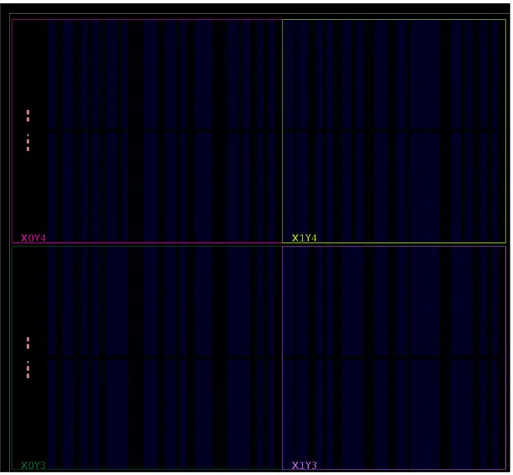
The elements within the FPGA are organized in columns. The most common structure is the one shown in figure 2.4, with one slice on each side of a routing switchbox, used to interconnect the different elements of the FPGA. One clock region is a tile formed by several columns of the same resource that span 60 rows of CLB columns, 24 DSP columns and 12 BRAM columns [17]. Clock regions are divided by horizontal and vertical clock routing and distribution tracks. Besides, the FPGAs also include a core column— integrating the System Monitor, configuration and PCIe blocks—as well as dedicated I/O banks, including high-performance GTH transceivers, I/O logic management and global clock buffers. The device view offered by Vivado, showing 4 clock regions in the KU060 device is depicted in figure 2.3
Figure 2.2: Two CLBs and one routing switchbox of the KU060 FPGA
2.2.3
FPGA configuration
The configuration of the FPGA for flash and SRAM FPGAs is stored in the configura-tion memory (CRAM) of the FPGA. It contains the logic tables for all LUTs, routing resources, interconnects, shift-registers, and flip-flops inside the FPGA, and is stored in a distributed fashion inside configuration latches or the distributed memory elements them-selves [18]. The other type of memory conforming a memory space in the FPGA is the Block RAM (BRAM) that provides the main accessible memory. It is utilized to store
Figure 2.3: Device view of the KU060 showing clock regions and columns within
user data, and is stored in RAM blocks with several customization parameters.
The types of FPGAs mentioned before are configured using a bitstream, that is, the bi-nary file that contains the configuration contents, along with all the necessary commands used to load it into the configuration memory of the device. For volatile SRAM FPGAs, support circuitry is included externally to launch the configuration automatically when the board is booted. For all Xilinx devices, including the targeted FPGA for this work, the minimum addressable unit of configuration is a frame, which in the Ultrascale tech-nology is composed of 123 words of 32 configuration bits. The total amount of frames composing the configuration memory is 37651 [19].
Each configuration bit affects the functionality implemented by the FPGA in some way. Thus, if any value of configuration is changed, its functionality is modified. In order to obtain the configuration bits that are utilized by the circuit, Xilinx offers the essential bits technology. The essential bits are defined as the ones used to define the hardware in the FPGA, and can be automatically reported during the elaboration of the bitstream in the form of a mask file: the “.ebd” file. This file has the same number of bits—in the form of characters, one representing each bit—as the configuration memory, excluding the contents of the BRAM memories. Besides, the dynamic soft values stored in shift-registers and flip-flops are never marked as essential, since their values may change during execution. Thus, the ebd file marks the configuration bits that belong to the design and must remain static for the correct functioning of the circuit. For the sake of simplicity, these bits are denominated configuration bits for the rest of this work.
Unlike the BRAM and registered values, configuration bits are not easily accessible for the user. When the circuit is functioning, there are three ways to access configuration memory: through JTAG, which is extremely slow, through the SelectMAP port, that needs an external device connected to the selectMAP pins to manage the communication, and the Internal Configuration Access Port (ICAP), which can be accessed by the internal logic. Apart from the JTAG connectivity, which is used to program the FPGA in most evaluation boards in the initial stages of a design by using a PC, the most used interfaces are SelectMAP for programming from a flash memory, or using external scrubbing and ICAP for partial reconfiguration and internal scrubbing applications. Regardless of the speed and internal or external nature of the ports, similar commands are issued to read and write configuration memory through them. A major difference is that, when using the ICAP port, all dynamic values stored in BRAM and registers are masked [19], so their values cannot be read. Besides, in the ebd file, these bits will never appear as essential. For more information on the Ultrascale family configuration, the reader is referred to [16]. Frame addressing
There are two ways to locate a particular frame within the configuration memory in Xil-inx FPGAs: the physical address, which is related to the position in the FPGA, and the linear address related to the position in the configuration memory. The physical address is composed by the following fields [19]:
Where the row address refers to the row in clock regions in which the frame is located,
Bits 25:23 22:17 16:7 6:0
Content Block type Row address Column address Minor address Table 2.1: Physical frame address format
from bottom to top and the column address refers to the major column formed by the same resource type, ordered from left to right. The minor address is used to select a frame within a major column. More details are provided in section 4.3.1.
The linear address is composed translating the position of the frame in the bitstream according to the configuration memory increasing sequentially. Its format is shown in the following table:
Bits 28-12 11-5 4-0
Content Frame linear address Word address Bit Table 2.2: Linear address format in the KU060 device
SEM IP
The Soft Error Mitigation (SEM) IP [19] is provided by Xilinx to help the user take advan-tage of the protection mechanisms integrated in Xilinx FPGAs for configuration memory: Error Correcting Codes (ECC) and Cyclic Redundancy Check (CRC) codes. They allow the IP to perform internal configuration scrubbing to correct errors, for example, caused by radiation. It uses two primitives:
• ICAP primitive: it automatically manages the ICAP access and commands needed to read and write configuration frames. The commands needed to write and read the configuration through ICAP are not documented, and no support is provided for other usage than integrated with the SEM IP.
• FRAME ECC primitive: manages the automatic checking of the ECC and CRC codes integrated in the readback CRC mechanism.
Even though little detail is given on how the primitives function or the ports they include, the general mechanism by which the corrections are performed is known: each configu-ration frame contains an embedded ECC code able to correct up to 4-bit errors inside a frame. Unlike previous generations of the SEM IP, such as for the 7th generation of Xilinx FPGAs, the ECC code used is not just a Single-Error Correction Double-Error Detection (SECDEC) code, but a more elaborated ECC-based algorithm whose capabili-ties are not clearly specified. When a frame is read through the ICAP, the ECC check is automatically done by the FRAME ECC. If the location of the error is detected, it is auto-matically corrected. Besides, it supports an additional classification capability when used in combination with an external memory that contains the .ebd file to indicate whether the affected bits were essential or not. This capability is not used in this work, since the injected bits are all essential.
There may be failures that are undetected or not corrected properly by using ECC, es-pecially if the error affects the ECC information itself, or it is a multiple bit error inside one frame that the ECC does not cover. To detect those cases, the whole configuration memory is covered by a CRC. The SEM IP repeatedly reads the configuration memory, calculating the CRC of the read frames one by one until the last frame is read. The calcu-lated CRC is then compared to the stored golden-CRC, which was previously calcucalcu-lated, before programming the FPGA. If they differ, the FRAME ECC and SEM IP flag a CRC error. However, those bits are not corrected by the SEM IP, and require further action by the user.
To test the scrubbing mechanism of the SEM IP, it includes the capability to inject an error in a configuration bit selected by the user. To do so, it reads the frame in which the bit is located, flips its value and writes it back through the ICAP. Besides, a command interface to connect the IP to a UART and control it externally is included. For more details about the SEM IP, the reader is referred to [19].
2.2.4
Upset classification and occurrence
The space environment, without the protection of the magnetic field from the earth, is extremely harsh. Apart from extreme temperatures and void, electronics have to deal with the undesirable effects produced by radiation. Radiation varies in energy depending on the elements that produce it, ranging from protons and neutrons to light and heavy ions coming from the sun, trapped in the earth magnetic field, or outside the solar system in the form of Galactic Cosmic Rays [20]. Its effects depend on two main factors:
• The Linear Energy Transfer (LET): depends on the particle producing the radiation. It is defined as the amount of energy deposited as it passes through a semiconductor, dXdE(M eV /mg/cm2) [21]
• The Fluence: defined as the number of particles per square centimeter that irra-diate the silicon [21].
The most significant effects that radiation produces can be summarized as:
• Total Ionizing Dose (TID): it is the amount of ionizing radiation that a particular device can stand until a functional failure, threshold shift, leakage current or timing change is produced [20]. Measured in krads, it is usually calculated for every mission, and then components and shielding are chosen so that they will withstand the expected dose.
• Single Event Effects (SEEs): they are caused by single particles that pass through the semiconductor material, inducing charge in the substrate that can cre-ate a current or voltage spike that may produce diverse effects[20]:
– Hard (destructive errors): when the particle produces a spike that creates a low-impedance path between power rails (latch-up), or a transistor source, a short-circuit is created, leading to the potential destruction of the device. These errors are denominated Single-event latch-up (SEL) or Single-event burnout (SEB). Besides, if the gate oxide is hit by a high-energy ion, it may break in the so-called Single-event Gate rupture (SEGR) [2]. All the hard errors are mostly destructive errors, with the exception of SEL, that may be recovered with a power cycle.
– Soft errors: alterations in a logical value in the device caused by a charged particle impacting a routing line, interconnection or memory cell. If the com-binatorial path of a device is affected, the event is called Single-event Transient (SET). When a SET propagates through the circuit and reaches a memory el-ement, or directly affects it, it changes the internal state and alter the data stored in that element. This event is a Single-Event Upset (SEU). Depend-ing on the amount of bits affected, they are divided between SDepend-ingle-bit Upsets (SBUs) or Multi-bit Upsets (MBUs) [2]. Some authors [22] distinguish between MBUs caused by a single particle, and coincident SEUs that effectively act as a MBU if they accumulate.
From a more practical point of view, a SEE is a fault in the circuit that, if propagated in the form of a SEU can cause the circuit to enter an erroneous state. Moreover, if this erroneous state alters the nominal behavior of the circuit and is propagated to an output, it is said that it caused a failure [23].
As CMOS technology is shrinking, new devices operate with reduced electrical margins, and gate oxide thickness is diminishing. As a consequence, the tolerance to SEL and TID is improving [20]. However, the SEU sensitivity is increasing, to the extent that they need to be taken into account for devices operating on the ground and not subject to harsh environments [24]. Hence, this work focuses in the latter, as SEUs are the most likely cause of failure due to radiation, as is also proven by the accelerated testing campaigns introduced below.
2.2.5
Radiation campaigns
In order to obtain the radiation sensitivity figures for a particular device, radiation cam-paigns are performed. FPGAs are exposed to a controlled source of radiation in terms of LET and fluence. Specialized installations such as Cyclotrons producing a range of particles such as neutrons, protons and heavy-ions are used for this purpose [25].
In those campaigns, the devices are loaded with test-implementations such as counters, shift-registers, and combinatorial elements such as multipliers and adders [26] [27]. How-ever, as complexity of the design increases, more complex designs are starting to be used in the FPGA to effectively reflect a more realistic scenario. Some examples are the us-age of the Soft Error Mitigation core (SEM IP) design from Xilinx, the Multi-Gigabit transceiver and Phase-Locking Loops (PLLs) in [28] and soft-processors in [25].
Different techniques are used to characterize the errors and effects of radiation. As men-tioned before, SEUs are the most common and main target of radiation campaigns. Be-sides, SELs and other destructive events are also observed and recorded. Originally, a whole device read-back of both configuration and block memory data was commonly used, which was then compared to the original bitstream [26], [27] [29] [4]. However, this tech-nique is extremely slow, since it requires disabling the clocks of the circuit—effectively freezing its state and masking potential errors—during the readback process, that lasts in the order of seconds [25]. This procedure allows to obtain“snapshots” of the SEU oc-currence in the configuration memory and to count the amount of ococ-currences. For the BRAM, usually a pre-defined pattern is loaded and then read back within the bitstream. Additionally, the power rails are monitored with current monitors to observe potentially destructive effects [27]. On top of that, the increase of current is also an effective metric for the SEU rate that configuration memory is subject to, since it creates spurious con-sumption sources by altering the device configuration and functionality.
More recently, new monitoring techniques are being used to obtain a finer-grain monitor-ing in the occurrence of SEUs and shiftmonitor-ing the focus towards observation of the functional behavior of the implementations subject to radiation. In [25], [30], a low-cost digital tester composed by an FPGA implements an FSM that provides input stimuli to the DUT-FPGA and checks the outputs and response of the functional units inside it. This enables monitoring events in the order of ns. The purpose of these implementations is
not to gather information about the vulnerability of the design itself, but to create DUT designs that have large and replicable logic structures, with state-spaces easily traversable that will produce observable SEUs. In [28], the DUT designs integrated self-checking fea-tures with status values that would be reported to an external monitor, and also remote monitoring is used to analyze the SEM-IP in [31].
Once results are collected, they are usually summarized in terms of the SEU cross-section (σ), which is obtained by dividing the total number of upsets by the fluence used in the test. It is usually reported in cm2/bit. Also the occurrence of SEL for a range of LETs
is reported, and sometimes the TID results. All that information is later used to evalu-ate the suitability for a particular device integrating certain technology for a given mission. It is important to consider that the probability of failure is both device-dependent— obtained in radiation campaigns—and design-dependent, thus, both need to be taken into account. In section 2.2.7, how to tackle the second factor will be approached.
2.2.6
Upset occurrence for the KU060 FPGA
The Radiation-tolerant Kintex UltraScale FPGA XQRKU060 [11], is the UltraScale KU060 device tested and qualified by Xilinx for it usage in space. With its release, Xilinx pub-lished results from radiation campaigns performed for its qualification in [32]. According to the results, it stands a TID of 100 Krad, and is immune to SEL until a LET of 80 M ev − cm2/mg. On the other hand, it has an expected SEU occurrence of 1.0e-8 upsets per bit per day for the configuration memory, and 2.7e-8 upsets per bit per day for the embedded block ram memory. Besides, a Single-Event Upset affecting a critical section of CRAM—such as a control state-machine— that causes loss of functionality, denominated Single-Event Functional Interrupt (SEFI) happens as often as 4.5e-4 upsets/device/day for Geostationary orbits.
Several additional and independent radiation campaigns have been performed in the reg-ular KU060 FPGA, and their results are here summarized:
NASA reports their results in [25], [30]. The obtained cross-section is 1.24e-09 cm2/bit for a LET of 20.4 M ev · cm2/mg, and 2.3e-15 cm2/bit for proton testing. They also report
the Mean-Fluence to Failure (MFTF) in particles/cm2, which is the inverse of the cross
section, and compare the Triple-Modular-Redundancy version of a counter synthesized in the KU060 to the same design—without TMR—in the radiation-hardened Virtex5QV, the current standard for high-throughput implementations. The results show that the UltraScale FPGA had a lower MFTF. Hence, being more vulnerable for the same LET, although the results were in the same order of magnitude, it shows potential for the non-hardened alternative. Besides, they compute the reliability of operation for a year from the MFTF and the expected particle flux per year. The results are shown for a MicroBlaze processor without cache, the same processor with cache and a simple counter, offering a reliability of 0.1, 0.7 and 0.87 for a fluence of 2.5e05 particles/cm2. These facts highlight
the relevance of developing mitigation techniques built in the logic, and the need to per-form a careful analysis of each design individually, since their vulnerability to radiation varies greatly even for similar circuits.
In [4], the cross section for different LETs is presented, and the one for protons is estimated to be 1.87e-15 cm2/bit for configuration memory, and 4.74e-15 cm2/bit for SRAM memory.
They extrapolate these results to In-Orbit rates using the CREME96 model, summarized in table 2.3. In [29], neutron and proton cross-sections are obtained, with results of 2.6e-15 for configuration memory (CRAM) and 4.5e-2.6e-15 for BRAM in the case of neutrons, and 2.5e-15 and 4.3e-15 for protons, all values expressed in cm2/bit.
Configuration Memory Block RAM per bit, per day 7.54e-09 2.48e-08 per device, per day 7.19e-01 6.26e-01
Table 2.3: In-Orbit SEU rate for CREME96 [4]
In [31], the cross-section of the SEM IP in the KU060 is analyzed by exposing the device to a proton flux while the SEM IP is running in the background, correcting any eventual SBU detected. The cross-section is recorded when an uncorrectable error is produced. The obtained cross-section is 5.91e-11 cm2/bit for CRAM. Besides, additional data anal-ysis is performed to show that only 0.07% of the SEUs cause MBUs, with 99.93% causing SBUs in CRAM. Additionally, the authors state that no MBUs in BRAMs were recorded in their testing. This fact confirms the statement presented in [33]: to enhance the pro-tective capabilities of SECDEC codes protecting BRAM and CRAM memory words in Xilinx FPGAs, the memory frames are physically interleaved.
In [28], the SEM IP is included in testing under proton irradiation, showing that it im-proves CRAM cross-section by a factor of 1.77, from 2.05e-15 to 3.63e-15 cm2/bit. On the
other hand, the usage of a SECDEC ECC code in BRAM drastically improved BRAM cross-section by a factor of 3272, from 2.52e-15 to 8.25e-12. These results back the ones presented in the previous paragraph, showing that the protection of BRAM is noticeably easier using ECC codes thanks to the low rate of MBUs when compared to CRAM. It is important to note that these results are based on proton irradiation, more applicable to Low-Earth Orbit (LEO). As a conclusion, the authors present LEO In-Orbit SEU rates (including previous results for heavy ions) for a device with 75% utilization excluding the Multi-Gigabit Transceivers. The results are 0.021 upsets/day, which improves to 0.001 upsets/day with memories using ECC and 0.00086 upsets/day using the SEM IP, rates that are acceptable for short LEO missions. However, the usage of SEM IP shall still be studied, since in [27], the only high-current events observed were related to a ScrubSEF I that would happen when configuration engine and critical registers such as the Frame Address Register (FAR) used for scrubbing and configuration readback were affected by a SEU. These events are only caused while scrubbing through configuration memory, as SEM does, and do not affect FPGA configuration. In the article, the authors present an alternative scrubbing method that would minimize such events.
To conclude, results presented in this section demonstrate three main facts:
• SEUs are the main source of failure due to radiation, and determine the expected reliability of a device operating in space. Few MBUs, SEFIs, SELs or destructive events have been registered, and are not expected in a regular mission.
• Apart from obtaining the expected SEU incidence for a specific device, it is essential to analyze the vulnerability of a particular design to SEU, since the final error rates
will vary greatly depending on both factors. This work aims to design a feasible methodology to do so for any particular implementation, without having to perform a radiation campaign for each mission.
• While BRAM is easier to protect with an ECC or TMR scheme, effectively reducing the error rate by several orders of magnitude, the CRAM is harder to protect. With the current solution offered by Xilinx SEM IP, it is not reliable enough for longer or more critical missions. The need to analyze the effectivity of other mitigation techniques, such as distributed TMR, recommended by NASA. The methodology presented in chapter 4 can also be applied with this goal in mind.
2.2.7
Previous work in SEU injection
Due to the high cost and effort required to perform a radiation campaign, several tech-niques for SEU emulation have been developed that allow to emulate the occurrence of a SEU by introducing an undesired change in a value, either in the user memory, registers or configuration memory. These campaigns allow to obtain a metric of the design sensitivity by counting the amount of configuration bits in a design that, when affected by an SEU, cause a functional failure. They are usually called critical bits, and are extremely useful to compute the reliability of a design. The sensitivity to SEU of a design is summarized by the Design Vulnerability Factor (DVF), which is obtained by dividing the amount of critical bits by the total amount of configuration bits used by the design. Multiple approaches to SEU injection have been presented in recent research:
• Injection circuits (saboteurs): introducing modifications in the component li-brary of a particular vendor, or using certain commercial tools that modify an initial netlist, these circuits allow a fast and effective injection for user memory [34]. These techniques are oriented towards user memory only, not acting in configuration mem-ory and being more suitable for ASICs. Besides, they need either specific tools or a great design effort, and add overhead to the logic in the circuit.
• Simulation-based injection: with this technique, errors are simulated rather than emulated [35]. Hence, the time required to inject enough errors makes this approach impractical as design complexity increases.
• Reconfiguration-based injection: based either on total or partial reconfigura-tion. A configuration frame is read, modified by flipping one or more bits to emulate a SEU and written back to the configuration memory. The approach based on total reconfiguration allows for more control of the internal states of the circuit and access both the configuration memory and the user memory through a total readback using JTAG [36]. However, that operation is noticeably slow, requiring a reported time of 916 seconds for 3000 bit-flips (around 3 bits flipped per second). For that reason, injection based in partial reconfiguration has become the most popular alternative [37], especially since the Internal Configuration Access Port (ICAP) was introduced by Xilinx, allowing for a faster reconfiguration. This work focuses on this last mech-anism for SEU injection, allowing injection of a whole design in a reasonable time, with an estimated time per bit of less than 5 ms per injection [38].
The usage of partial reconfiguration for error injection can use any of the configuration ports provided in Xilinx FPGAs: external ports, i.e., the JTAG configuration port, the
SelectMAP configuration port and the ICAP. The most suitable choice is ICAP, due to the speed achievable compared to its counterparts [38]. The main limitation when using partial reconfiguration to inject errors is that they are only meant to act in configuration memory: as explained in [38], the information stored in a FF is not modifiable after the initial programming operation using the configuration memory unless the sequential logic is reset. Thus, a careful process such as the one detailed in [38] is needed to manage the individual resets. Another alternative is presented in [21], using injection through partial reconfiguration, and a structural approach, this is, adding injection inputs manually to all flip-flops in the design using a parser and the design netlist.
Even though the data that can be collected is limited by the fact that no injections can be performed in BRAM memory and flip-flops, injection by partial reconfiguration is the current mechanism used to compute device sensitivity to SEU. The main reason for this is that it is the most practical mechanism when approaching complex circuits, which does not require any specific tool or manipulation of the circuit, is being able to assess its sensitivity as-is, without any additional logic that may alter the results. The obtained sensitivity will be lower than the real one for devices that have a high utilization of BRAM memory, but, even in that case, the SEU injection is accurate when used to obtain the relative sensitivity that results of implementing mitigation techniques in the circuit, and can be used as a tool to assess the effectivity of these techniques [39].
Apart from the method used to inject errors, it is interesting to reflect on the different mechanisms used to check for functional failures. These partially depend on the type of circuit tested:
• Golden-model: consists in running two instances of the same circuit in parallel. One is the Device Under Test (DUT), in which the injection will be carried out, and another one is the golden reference or model. This approach is commonly used combined with a set of test-vectors that are used as the inputs of both circuits. Then, the outputs are compared, and, if they differ, an error occurred in the DUT. Its main advantage is that it is not hard to implement, provided that an automatic tool is used to generate the test vectors with a good internal-state coverage and that the visibility of errors cannot be affected by the error itself. As a disadvantage, it only allows a limited understanding of the errors, since they can only be detected in the output. Hence, it works properly for circuits that perform a bounded calculation, but not for the case of a module implementing a communication protocol that could mask a significant amount of failures. It is the approach followed in [40], [21], [41], [42].
• Stand-alone with internal monitoring: consists in instantiating just one DUT, and monitoring internal signals or registers and outputs to gather more information about potential failure modes. It is a suitable approach for circuits that include Quality-of-service (QoS) mechanisms already integrated that allow for error detec-tion, or if an automatic mechanism to detect failures by examining the internal registers of the circuit is feasible and simpler to implement than duplicating it. Its main advantages are the reduction in the amount of logic needed, allowing for test-ing bigger DUTs and less intrusive logic that will have less impact on the results. Besides, it is able to detect failures that would be masked in the output in circuits that include error correction or QoS mechanisms. On top of that, as explained at
the end of this section, it is the most suitable approach for verification purposes. [23]. Its main drawback is that, potentially, some internal errors could be masked by the errors themselves. This risk can be minimized by continuously recording the monitored signals and not allowing errors to be introduced in the data generating and checking blocks, which will still be able to detect the most relevant functional errors. This approach will be the one used in this work, and was also used in [43]. • Mixed approach: finally, combining both techniques described above is also
pos-sible. It provides the most reliable mechanism when it comes to detecting any error or deviation from the expected behavior, allowing for high detection granularity. However, it comes at a very high logic cost, allowing to test DUTs of a constrained size, and altering the occupation of the device in a significant way, which can also introduce differences in the behavior of the circuit against SEUs when compared to a stand-alone implementation. Besides, although uncommon, SEFI events at FPGA level may still mask some errors and cause failure in both DUT and golden model by affecting, for example, the global clock routing. This is the approach used in [39].
Once the mechanism for error injection and correction has been obtained, in literature there are two main approaches to compute a design’s sensitivity:
• Following the same approach used in radiation campaigns: injecting errors in ran-dom locations of the configuration memory. This approach, used in [39], [42] allows to obtain the average amount of injections needed for the device to fail. It is effec-tive when used with a model of the expected SEUs, and its main advantage is that it does not need the data from radiation campaigns to estimate the reliability of a particular circuit. However, this method is not comprehensive, in the sense that it will leave configuration bits without analyzing them, so potential vulnerability points will remain unknown.
• Systematically injecting errors in all locations of configuration memory that belong to the DUT. This approach is used in [21], [43] and [40]. This method allows for a comprehensive analysis of all potential vulnerabilities related to configuration memory for any particular implementation, and for a more precise calculation of the DVF. Its main drawback is that it requires data from radiation campaigns performed in the same device to draw conclusions about the absolute reliability that can be expected for a particular mission, and that might be to slow in bigger designs. Although several differences have been presented, all the works analyzed have a similar methodology in common. The usage of partial reconfiguration to inject errors in configu-ration memory is done either through the SEM IP from Xilinx [21, 40] or through means of a custom reconfiguration controller [41, 39, 42]. The injection consists in flipping one bit, emulating an SEU, except for the case of [41], which is the only work that focuses on MBUs. The reason of focusing on SBUs is that those are the most common events—as shown in section 2.2.6. After the error is injected, the circuit is kept running until it performs a particular operation and a set of outputs are available. For the sake of veloc-ity,when errors are observed in the outputs they are corrected by writing back the original word to configuration memory. Only in [39] and [40] a full device reboot was performed to ensure the error correction.
2.3
Space Fibre
This work is closely related with the SpaceFibre technology. In this section, a short introduction to its basic concepts is shown. For the sake of brevity, most details and several capabilities of SpaceFibre are omitted. Hence, the reader is referred to the ECSS standard [3] for more information. SpaceFibre is a high speed serial link based network standard defined for on board spacecraft usage. SpaceFibre specifies the physical layer for both electrical and fibre optic medium. In the electrical medium, which is the one used in this work, Gigabit serial transceivers are used to serialize the data and transmit it. In particular, GTH transceivers from the KU060 FPGAs are used for the injection campaign.
2.3.1
Gigabit serial transceivers
The main component that SpaceFibre relies on is a transceiver capable to achieve line rates in the order of gigabits per second. These transceivers are becoming increasingly used onboard spacecrafts to transmit the huge data generated by the latest generation of instruments and sensors. Originally, they were not designed with the space environment in mind. Hence, additional protocols that ensure QoS such as SpaceFibre are needed. The basis of this transceivers lies in a SerDes element, which transmits a data word bit by bit at an extremely high rate. To do so, the SerDes uses a fast reference clock—125 MHz in this work—and several Phase-Locked Loop (PLL) circuits that are able to generate clocks whose frequency is a multiple of the reference clock and whose phase varies in a controlled manner, and transmit the data aligned to the flanks of these faster clocks, reaching line rates in the order of the gigabits per second. Only two differential lines are used: the TX and the RX line. At the rates used by gigabit transceivers, transmitting the reference clock in a separate line is not practical. However, from the values transmitted through the lines, the phase of the reference clock can be aligned at the far-end, to be able to appropriately sample the input values at the rigth moment. These values then de-serialized and provided with a lower clock rate in parallel words. Apart from a reference clock and high-performance PLLs to align it, there are other elements that allow the successful transmission of data at such a high rate. Two of the most relevant, and whose usage is required by SpaceFibre are listed here:
• Differential signaling: the GTH transceiver uses LVDS in current-mode, which drives two parallel lines that encode the transmitted bits in the differences in voltage in the line. The lines are terminated with a resistor to maintain a constant value of current flowing between receiver and transmitter. Therefore, the generated magnetic fields cancel each other, significantly reducing the emissions. Besides, the noise affects both voltage values equally, and its effect is cancelled when obtaining the data encoded by the difference in voltages.
• 8b/10b encoding: in order to be able to recover the clock from the data trans-mitted in the line, the voltage should resemble a typical digital clock as much as possible. Hence, data is encoded with 8b/10b aiming to minimize the consecutive bits that have the same voltage, maximizing its variation. To do so, the encoder maps every 8-bit symbol to a 10-bit symbol, defining two alternative symbol map-pings for each 8-bit value. The symbols are selected to ensure that no more than 5 consecutive bits have the same value to facilitate clock recovery, and that the total
difference of 1s and 0s transmitted is lower or equal than two, to ensure DC bal-ance, which minimizes noise and bit errors. Besides, the remaining values are used to define special control characters, the comma character being the most relevant one. It is a character that cannot be obtained by partially concatenating any other characters in the serially received bitstream. Hence, when detected, it marks a byte boundary used to align the received bytes correctly.
2.3.2
Space Fibre modules
As a network protocol or standard, SpaceFibre is divided into layers of abstraction that implement certain functionality as described by the protocol description in [3]. A Space-Fibre link is composed by one or more physical connections, called “lanes”. SpaceSpace-Fibre is capable of transmitting data in parallel through different lanes to increase its throughput. However, this work focuses in the single-lane mode with a throughput of 2.5 Gbps, which is enough for most applications. The layers for a single lane are the following: applica-tion, network, data link, lane and physical. They are shown in figure 2.5 The application layer is defined by the implemented system. Only its interface with the network layer is defined, establishing how data and broadcast words shall be transmitted to SpaceFibre. The physical layer is composed of the SerDes, drivers, cables and connectors, and the IP that implements the 8b/10b encoder and the synchronization and clock correction buffers according to the standard. The network layer—describing the routing and transmission between nodes of packets and broadcast messages—is not fully implemented in the Space-Fibre IP port, which is designed to receive and send data over a single link. The only functionality implemented is the conversion of packets and broadcast messages to N-chars and fills used in the data link layer. Therefore, this section introduces the data link and lane layers, which are the most relevant for this work. The SpaceFibre IP implementation divides the functionality of the data link layer in the virtual channel layer and retry layer: • Virtual channel layer: a SpaceFibre virtual channel is an independent channel that can carry information across a single link in parallel with other independent, information carrying channels [3]. It is equivalent to a SpaceWire channel or link (terms with equal meaning in the SpaceWire protocol), with the term “virtual” used to highlight that a SpaceFibre link can contain several multiplexed SpaceWire channels used by different applications to transmit and receive data. One of the aims of SpaceFibre is to be compatible with SpaceWire. Hence, the virtual channels in SpaceFibre follow the same packet format as the channel in a SpaceWire link. The virtual channel layer is in charge of managing the medium access control, deciding which virtual channel transmits data depending on the allocated bandwidth and the amount of received flow-control tokens. The flow-control tokens indicate the amount of free space in the receiving buffer of the far-end, to ensure that no overflow and data loss occurs—. Other additional capabilities are the capability to define scheduling and precedence between virtual channels. The input and output buffers, one for each virtual channel, are located in this layer. On top of that, since several virtual channels may share a physical link, a virtual-channel de-multiplexer is used in the receiver part to drive the received data to the appropriate buffer. Data to transmit is encapsulated in frames, and passed to the lower layer. Finally, next to this layer, the broadcast layer is implemented, managing broadcast information that is passed directly to the lower layer.
![Figure 2.1: AMBA bus master and slave multiplexing [1]](https://thumb-eu.123doks.com/thumbv2/5dokorg/4254530.93964/17.892.181.729.119.517/figure-amba-bus-master-slave-multiplexing.webp)
![Figure 2.4: Types of Single-Event Effects. [2] p. 4](https://thumb-eu.123doks.com/thumbv2/5dokorg/4254530.93964/24.892.125.769.864.1105/figure-types-single-event-effects-p.webp)
![Figure 2.5: SpaceFibre Protocol Stack. [3] p. 36](https://thumb-eu.123doks.com/thumbv2/5dokorg/4254530.93964/33.892.243.656.718.1090/figure-spacefibre-protocol-stack-p.webp)