INOM
EXAMENSARBETE
TEKNISK FYSIK, AVANCERAD NIVÅ, 30 HP
,
STOCKHOLM SVERIGE 2016
Approaching micrometer size
graphene flakes on an insulating
substrate with STM
KIM AKIUS
KTH
TRITA TRITA-ICT-EX-2016:15
Master of Science in Engineering Thesis
Approaching
µm size graphene flakes on an
insulating substrate with STM
Kim Akius
Supervisor: Professor Jan van Ruitenbeek, Leiden University Examiner: Professor Mikael ¨Ostling, Royal Institute of Technology
Royal Institute of Technology, SE-106 91 Stockholm, Sweden Stockholm, Sweden 2015
Typeset in LATEX
Graduation thesis on the subject of Nanophysics for the degree of Master of Science in Engineering from the School of Engineering Sciences.
TRITA-ICT-EX-2016:15 ISSN
ISRN
© Kim Akius, 2016
Abstract
In this study, a method for landing with a Scanning Tunneling Microscope (STM) on aµm size flake of graphene was developed. Two approaches were explored, one using physical guides to navigate on the sample and another one using capacitive pickup in the system. We show that with no modification of the STM that was used, we could land on a micrometer size flake of graphene.
Preface
This thesis internship was carried out in Jan van Ruitenbeek’s research group on Atomic Molecular Conductors at Leiden University in the Netherlands.
The thesis is divided into 5 chapters: an introduction to the problem and motivation on the work. The second chapter is chapter on the background of STM and graphene, followed by a chapter on the method. Finally the results are presented and summarized.
Acknowledgements
First and foremost, I would like to thank my supervisor Professor Jan van Ruitenbeek for bringing me into his group with such open arms and given me constant support throughout the project.
I want to thank Sumit Tewari for all the day-to-day support, discussions, banter and help. I have every single day of my project come to him with at least one dumb question, often ones I already asked the day before. He has remained patient with me and still listened to my suggestions and was also willing to completely change our approach mid-way, despite my lack of previous experience with working with STMs. I also want to thank Dr. Federica Galli for all technical support and encouragement she has offered throughout my project in spite of me constantly interrupting her work. The samples we have used were fabricated by Gaurav Nanda who i also want to thank. He works in Professor Paul Alkemade’s group at the Kavli Institute of Nanoscience at TU Delft. I also want to thank Sander Blok and Dr. Amrita Singh for help with sample preparation.
I would also like to thank everyone in the Leiden Institute of Physics for making me want to stay in science, including Dr. Carlos Sabater, Dani¨el Geelen, Alexander van der Torren, Marcel Hesselberth, Dr Aniket Thete, Dr. Johannes Jobst, Dr. Milan Allan, Irene Battisti and Koen Bastiaans. You’ve made the days in the meethaal a pleasure!
I want to thank my family for their constant support throughout this degree, despite my sometimes completely disappearing into my books.
Finally, I want to thank Madeleine for her unconditional support.
Contents
Abstract . . . iii
Preface v Acknowledgements vii Contents ix 1. Introduction and motivation 3 2. Background 5 2.1. Scanning Tunnelling Microscope . . . 5
2.2. Capacitance in SPM systems . . . 6
2.3. Graphene . . . 7
3. Method 9 3.1. Capacitive STM for finding conductors . . . 9
3.2. Principle of operation . . . 9
3.3. Search Algorithms . . . 10
3.3.1. Li et al . . . 10
3.3.2. Saddle point method . . . 12
3.4. Experimental details . . . 13
3.5. Coarse XY-stage . . . 14
4. Results 17 4.1. Final Sample design . . . 17
4.2. Line and box scans . . . 18
4.3. Successful landing on graphene . . . 22
5. Summary and Conclusions 25
Bibliography 27
Chapter 1
Introduction and motivation
Every now and there is a spark in science that results in an explosion of excitement, antic-ipation and funding into a certain direction of research. One terrifying example is nuclear research in the 1950s following the dawn of quantum mechanics and relativity. DNA re-search in the 2000s sparked by the mapping of the human genome in 2003 marked another decisive shift, bringing promise of a deeper understanding into our heritage and how it relates to our illnesses and frailties.
Nanoscience experienced an explosion of this kind in the 1980s with implications in most physical science disciplines, including physics, chemistry and biology. This time Gerd Binnig and Heinrich Rohrer had invented the STM [1]. The following years saw rapid development of Scanning Probe Microscopy (SPM) technologies including STM, Atomic Force Microscopy (AFM) and derivatives thereof. Atomic resolution STMs became a reality. STM has since been called for nanoscience what the telescope was for astronomy [2]. A Nobel prize was awarded for Binning and Rohrer’s discoveries and new era in the science of everything small had begun.
Andre Geim and Konstantin Novoselov created a similar spark in 2004. Their discovery, Graphene, predicted decades earlier, had for the first time been isolated in a lab [3]. The worlds first 2D material had been discovered, with many soon to follow, and would soon be commonly referred to as a wonder material due to its multitude of fascinating properties. Graphene has an electric field effect, the phenomenon transistors have relied on to form the basis of the computer revolution of the last 50 years. For decades people had been search-ing for the material to replace silicon followsearch-ing the breakdown of Moore’s law. Although graphene most likely will not replace silicon due to the absence of a band gap, it is still a field of research that gathers a lot of attention, enthusiasm and interest. A Nobel prize was also awarded for Geim and Novoselov’s discoveries. This marked the beginning of new era of research within carbon, graphene and perhaps more importantly, 2D-materials.
This paper will explore a very small subsection of each of these topics and their overlap. The project set out to find a reliable method to locate a small,µm-size, flake of graphene on a insulating substrate. The difficulty of this lies within an inherent limitation of the STM. It relies on the quantum mechanical phenomenon of electrons tunnelling through a potential barrier, in this case a vacuum or air, between two conductors. The conductors are a metallic, sharp tip, and the substrate to be scanned. And therein lies the limitation - the substrate needs to be a conductor. For large pieces of graphene this is not an issue, commercial tools can routinely deposit cm-size films of graphene upon an arbitrary substrate using Chemical Vapour Deposition (CVD) and wet transfer methods as developed in Ruoff’s lab in Texas [4]. However, commonly in physics, when we study very large systems, we gain
4 CHAPTER 1. INTRODUCTION AND MOTIVATION knowledge of aggregate behaviours but loose microscopic detail and often with it, insight into the microscopic mechanism of what is actually happening. The microscopic detail of how electrons behave in graphene, is washed away in the mighty Fermi sea.
This research was conducted in the group Atomic Molecular Conductors (AMC) and the motivation of the study is the research areas within this context. In such research, one often needs a nanometer sized gap, a nanogap, between to conductors. One very successful ap-proach to create these nanogaps is that of mechanically controlled break junctions (MCBJ) pioneered by the supervisor in this project, Professor Jan van Ruitenbeek. Another method for creating these nanogaps is electromigration, also a research theme in the group for which the results can hopefully be used. Further the group hopes to utilize the methods developed in this project for use in a new novel methodology of nanogap formation using a Focused Ion Beam [5].
Chapter 2
Background
This chapter is meant as a introduction to the STM and graphene. As mentioned the STM was invented in 1981 and it was awarded with a shared nobel prize together with the elec-tron microscope. It was incredibly important in laying the foundation for SPM and it is still one of the preferred technologies for studying electronic properties at a atomic level. A brief discussion on the working principle of an STM will follow. For a more exhaus-tive discussion, Julian Chen’s Introduction to Scanning Tunnelling Microscopy [6] is highly recommended. Further generally many books in nanotechnology such as Bharat Bhushan’s book on Nanotribology [7] contain excellent overviews of SPM techniques. Kalinin and Gru-vermans work on SPM in general including a chapter specifically on Scanning Capacitance Microscopy is also recommended, especially the introduction [8] containing an extensive list of different types of SPM.
2.1
Scanning Tunnelling Microscope
Figure 2.1: The model of STM used in the project, Jeol JSPM 4500A, note the coarse approach motors protruding from the right chamber on the bottom right chamber. Image from Jeols website.
The quantum phenomenon of tunnelling is very sensitive to the distance between the electrodes, in this case the sample and the tip. Sub-nanometer changes in the tip sample
6 CHAPTER 2. BACKGROUND separation gives a noticeable change in the current. Thus, by monitoring the current while moving along the surface, one can get very precise information about how the separation between the tip and the sample changes. By doing this along a line and recording the current one can obtain a surface profile. Adding many of these types of surface profile lines together, or scanning the surface, is collectively called Scanning Probe Microscopy. However, there is a high likelihood of the tip-sample separation changing drastically even within a small radius of one point on the sample, so moving quickly across the sample can cause the tip to crash into the sample. This could ruin the tip and even the sample, so surface roughness or even the sample is not being mounted perfectly perpendicular to the tip could ruin an experiment. To overcome this first problem of crashing into the surface, one can add to the system a height control and monitor the current. If the tip gets too close to the sample, the current will rise and one can simply retract the tip a little bit from the surface. To automatize this one chooses a reference current (corresponding to a tip-sample distance), and uses some electronics to continuously measure the current and adjust the height to keep the current and thus the tip-sample separation at a constant value. In STMs this is realized with a feedback system and is used with the height control facilitated by piezo motors. The feedback system is usually utilized in such a way that the tunnelling current is kept constant, constant current mode, and recording the Z-piezo extension as the line profile. Other set-points parameters are also possible. To summarize: we use a feedback system with piezo motors to keep the current to a fix value, keeping the tip-sample separation large enough for the tip to not crash into the sample and still stay within the tunnelling regime. In modern STM systems, the controller is a single point interface between the computer that the STM operator (aka the “physicist”) uses to manage the hardware of the STM, including the feedback system, piezos, coarse motors, and bias lines.
2.2
Capacitance in SPM systems
The approach here focuses on differences in capacitance rather than absolute values of it so capacitance will be used loosely to mean difference in capacitance. Further capacitive pickup from the background (tip-holder, stage etc.) will not be covered thoroughly, The concept of utilizing the capacitance in SPM systems was conceived soon after the first STMs and AFMs in the mid to late 1980’s [9–11]. It remained a somewhat peripheral scanning technique compared to the most common SPM modes such as the useful non-contact AFM and constant current STM for very high resolution imaging on conductors. However, with the growth of the semiconductor industry the Scanning Tunneling Microscope (SCM) was found to be a very useful tool to probe p/n doping in semiconductors [12–14]. The seemingly most common type SCM is essentially an AFM with a conductive tip. It is mostly used at very small tip-sample separation [8]. The literature discusses SCM resolution [15–17] and other conventional SPM characterization.
The mode used here uses a slightly different approach where the scanning is mostly at a larger tip-sample separation (a few micrometers). Note that the technique developed is not intended to create an image as is done in normal SCM (and SPM in general), but rather just to use the capacitance as a navigational tool. Therefore the it is strictly not an SCM implementation but rather could be viewed as a capacitance assisted approach method for conventional STM.
The capacitance of a system often depends strongly on the geometry of the system and that is also the case here. In an AFM the tip is often in effect a small protrusion on a semiconducting material such as silicon. The whole bulk of this silicon chip, therefore
2.3. GRAPHENE 7 influences the capacitance. How large this effect can qualitatively be understood of in terms of the ratio
AR = dts dbs
(2.1) where dts is the tip-sample separation and dbsis the bulk-sample distance. In a AFM this
ratio is quite small as the bulk of the cantilever and the bulk chip behind it is very close to the cantilever tip itself, in the order of hundredµm. In an STM system this ratio is larger due to the geometric shape of the tip geometry where the tip often is very sharp and is mounted perpendicularly to the sample.
In an STM however the ratio between the tip-sample separation and the tip-holder. Thus the background effect will not be as localized to the tunnelling junction as in a AFM. That is not to say that the background will not still have a large effect on the signal, just that it should vary more slowly. Apart from background effects, the system geometry is essentially given by the tip-sample separation, d, and the geometry of the tip itself. Intuitively the capacitance shows an inverse relationship to d just as in a parallell plate capacitor. [15] Just as in the conventional STM, shape of the tip influences the capacitance. The most common parameter used to characterize STM tips is the tip radius of curvature, r and wire thickness. As would be expected, a large tip radius means a larger capacitance, again similarly to a parallell plate capacitor. [15]. For very large tip radius it actually converges towards the parallel plate model. [12] To obtain a very sharp tip, the established method is to electro-chemically etch a tip, often made of W or PtIr, sometimes followed by annealing [2, 18–20]. In this project a commercial electrochemically etched tip is used. Let’s summarize:
δc(s) = (
1/s if s >> 200 nm
α ln(s) if s > 200 nm (2.2) where α is some constant and δ indicates that we are looking at changes in capacitance. Only the region where s is much larger than 200 nm is relevant here. However, it is interest-ing to note that the tip sample capacitance changes it’s behaviour there. This change could potentially be utilized to implement a faster approach to a normal STM system [15]. One such implementation would be to very quickly approach the surface while continuously mea-suring the capacitance. Once the ln(s) behaviour is observed one slows down the approach to a normal approach, using the change as an indication of sample proximity. RHK, a large STM manufacturer, has presented a new approach method utilizing the capacitance, how-ever the details have not yet been publicized apart from a video. Given the content in the video one could speculate that this is indeed what they are trying to implement1. Although
our STM controller was indeed a RHK brand controller, unfortunately this procedure was not implemented in our system yet.
Note that the difference in height in different regions of the sample will contribute to the signal. Effectively, where the gold is deposited, d will be reduced by whatever the thickness of the gold is. It will be a marginal change as d will be on the order of µm and the gold patch is usually a fraction of this, but nevertheless. For this reason and to facilitate easier wire bonding with less chance of leak currents after bonding, a rather thick gold layer is recommended.
2.3
Graphene
Once thought to be unstable [21], was isolated in 2004 [3] and the many facets of it’s rich electronic properties have been thoroughly discussed ever since.
8 CHAPTER 2. BACKGROUND
Figure 2.2: Graphenes electronic dispersion with a zoom in of one of the symmetry points (commonly K, K0 in the Brillouin zone or dirac-points), from [23]
Graphene is a atomically flat, carbon allotrope with a hexagonal atomic lattice structure. It has σ bonds (hybridized sp2) bonds in the plane, between the carbon atoms and π bonds
out of the lattice plane. The σ states have a large band gap, however the π orbitals have a conical connection at the K and K0 points, precisely at the Fermi energy [22, 23]. Many of
graphenes esoteric properties can be understood in terms of these π orbitals. A consequence of the conical points is that graphene is a zero gap semiconductor, meaning that it has a completely filled valence band and a completely empty conduction band.
Highly Ordered Pyrolytic Graphite (HOPG) is a common substrate for STMs due to being readily imaged at atomic resolution. The reason for this is that STMs probes the electronic orbitals of substrate and HOPG has localized, out of plane orbitals making the atomic resolution easier to obtain.
Much more can be said about graphene and it’s electronic properties, whether it is the stronger than diamonds in plane bonds or it’s higher conductivity than copper, room tem-perature Quantum Hall Effect, or it’s massless Dirac electrons. Although this project set out to make studies of graphenes exotic properties possible graphene itself will unfortu-nately not be covered in any detail and limited to the purpose of this paper. For a more in depth exploration Katnelson’s book, Graphene, Carbon in Two Dimensions [22] and Castro Neto’s article, The Electronics Properties of Graphene [23] from 2009 are personal recommendations.
Chapter 3
Method
3.1
Capacitive STM for finding conductors
The method developed is strongly inspired by the paper by Li and colleagues [24]. The idea is to use the capacitance of the tip-sample system to navigate to the graphene flake. Thereafter the next section presents the principle of operation followed by some discussion on critical points of the technique.
3.2
Principle of operation
The tunnelling current in an STM is given by the equation:
I = GV (3.1)
where G is the tip-sample conductance, V is the bias applied between sample and tip, and I is the current as measured by the STM controller (after pre-amplification). The conductance here is very short range. Now, if we apply a AC current instead of a DC we add an additional term in the current:
˜
I = G ˜V + iωC ˜V (3.2) where ω is the angular frequency of our AC current and our tildes indicate alternating currents, C is the capacitive pickup. Now, C is a longer range effect than tunnelling, enabling the methodology to be used at much larger distances than the tunnelling regime. So to summarize, this method relies on two main points:
1. Locally large electric field gradient near the edge of the top plate 2. Long range interaction due to modulated bias
The capacitance of this system with the tip will as usual depend on the electric field. The tip shape and tip-sample separation will also affect the capacitance but for the purposes here, we do not need to worry too much about either of these effects. As mentioned, the capacitance will not be used in a quantitative way, it is only used qualitatively to see if it is increasing or decreasing. In the region close to the edge of the smaller plate, the electric field with have a large gradient parallel to the plate as indicated by the red arrows in figure
10 CHAPTER 3. METHOD
Figure 3.1: (a) Tip-sample-substrate layout. (b) Circuit diagram of the STM-sample-controller circuit. (c) Electric field around a thin conducting plane, such as a gold electrode on on an insulator. (d) Electric field around the same electrode, only now with the back gate (silicon in our case) grounded. (e) The same system but with the back gate at -1 V and the front electrode at +1 V. Courtesy of Li et al[1].
3.2 (e). That is to say that the spatial component ∂E
∂x is large in the vicinity of x = a where
a is an edge of the the smaller plate (x parallel to the substrate and plate). This means that from the perspective of the tip, moving the tip parallel to the sample, it will hopefully see a large variance in the capacitive pickup as measured by the lock-in amplitude.
3.3
Search Algorithms
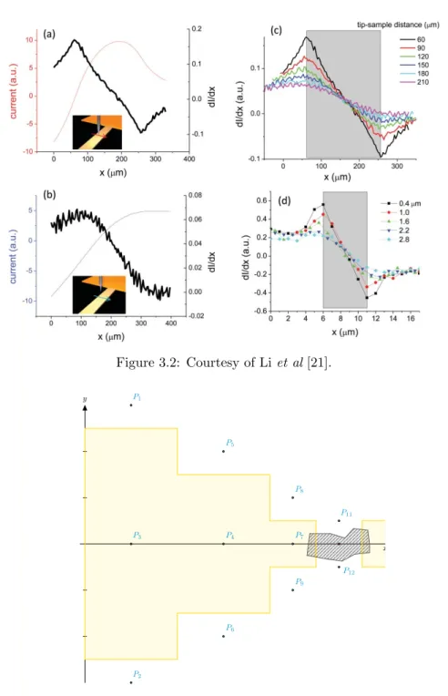
The method used to find the graphene patch differs in some details compared to Li and colleagues. To see how they differ, let’s first summarize their method. To illustrate this method more clearly, see figure 3.3 and references to points therein.
3.3.1
Li et al
1. Place the STM tip on one side of the largest gold electrodes, for example point P1.
Move the tip across the electrode (in the y-direction) to P2. Signal will increase and
then starts to decrease once the tip has passed the the middle of the electrode, P3.
By taking a numerical derivative of the obtained lock-in amplitude, a distinct minima and maxima is obtained, corresponding to the edges as in figure 3.2 (c) and (d).
3.3. SEARCH ALGORITHMS 11 Figure 3.2: Courtesy of Li et al [21]. P3 P4 P5 P6 P7 P8 P9 P11 P12 P1 P2 x y
Figure 3.3: Fictive sample for purposes of illustration. Points, Pi, refer to method
explaina-tion for Li et al.
2. Once edges are located, move tip onto a point on the gold patch, for example P3 and
approach as in normal STM operation. Once tip has approached tunnelling is verified, retract the tip to a distance, d, from the surface. This distance needs to be chosen with care because the characteristic peak due to the edges flattens with increasing
12 CHAPTER 3. METHOD tip-sample separation.
3. After the tip has been retracted to d above the surface, move along the x-direction onto the smaller patch, for example to P4. With a well characterized coarse motor,
this should not be a problem. Once the tip is above the second patch, move to the side of the smaller patch, for example to P5. Go across this electrode to P6 while
measuring the lock-in amplitude, obtaining a new curve with a maximum when the tip is somewhere over the central region of the patch. Taking the same numerical derivative over this smaller patch, they get an indication of the edges of this new patch, just as earlier.
Iterating these steps, making sure to stay close enough to the sample to still get a sharp edge in the capacitive curves, they can move from a larger patch to the next smaller one, until they are on the last patch.
With this method, for the fictive sample in 3.3, one has to perform 4 capacitive mea-surements, going from P1to P2, P5to P6, P8to P9and finally P11to P12. Additionally this
method requires a normal STM approach for each subsequent patch, including the graphene patch, resulting in 4 approaches in total (the points along the center line in the sample).
3.3.2
Saddle point method
A similar method with the benefit of being faster due to fewer approach steps and having fewer post-processing steps of data (no numerical derivation), is described here. Let’s call this method the Saddle Point method for reasons that will become apparent. Points, Pi
here refers to the points in figure 3.4.
P3 P1 P2 P4 x y
Figure 3.4: Points, Pi, refer to method explanation for Saddle Point Method. In summary,
one capacitive scan is taken from P1 to P2, one from P3 to P4 to obtain a saddle point
3.4. EXPERIMENTAL DETAILS 13 1. Place the STM tip on one side of the largest gold electrodes, for example point P1.
Move the tip across the electrode (in the −y-direction) towards P2. Signal will increase
and then start to decrease somewhere in the vicinity of P3. When a clear negative
derivative of the current has been observed, the coarse motor movement is reversed until the tip has returned to the maximum current value.
2. Approach the tip to the surface and verify tunnelling. Once tunnelling is observed, the tip is retracted only a few µm.
3. Moving the tip in the x-direction, the current is expected to: first decrease as the capacitive pickup will decrease because the patches get narrower. Once the patches get larger again, the capacitive pickup will increase again when the patches get wider on the other side of the graphene. So moving the STM tip from P3to P4, the current
increases and once it starts to decrease, the coarse motor is reversed and the tip is returned to the minimum. Another, optional sweep in the ±y- and ±x-direction can be performed to verify the saddle point.
4. With the tip over the current saddle point, maximized in y and minimized in x, a safe approach to the graphene patch can be performed.
So the differences in the methods is essentially that one is a iterative, methodical searching for edges with post processing to obtain derivatives. Approaching on each patch doing a full line scan across each patch and taking numerical derivatives of them is rather time consuming. A normal STM approach can take from a few minutes to several hours, espe-cially without optical access. For our method only two approaches are necessary and fewer capacitive scans are required. Of course, by only retracting a few micrometers from the surface and then walking mm distances does require a fairly flat mounting of the sample as a small tilt would cause a tip crash. These issues are also addressed in Li’s paper. During the testing of the method however, no crashes were recorded and many approaches with the indicated maximums as the only guide were successfully carried out. To summarize the method will rely on a modulated signal with 180 degrees phase shift on the back plate compared to the front electrode. Further a lock-in amplifier is used to get the sum of the two applied, modulated biases. The algorithm for the actual approach has been design in such a way to try to minimize the number of Z-approaches in what we call the Saddle point approach.
3.4
Experimental details
The samples are fabricated using standard graphene device fabrication methods. The graphene is exfoliatiated from HOPG and deposited on a silicon wafer as pioneered by Geim and Novoselov [3]. When a flake has been localized, gold electrodes are deposited using elec-tron beam lithography processing. The samples are thereafter characterized with Raman spectroscopy to ensure the quality of the flake and the number of layers of graphene. Raman spectroscopy is a very popular method to characterize graphene as it gives an indication of the number of layers and the amount of crystalline defects as well as contaminations [25].
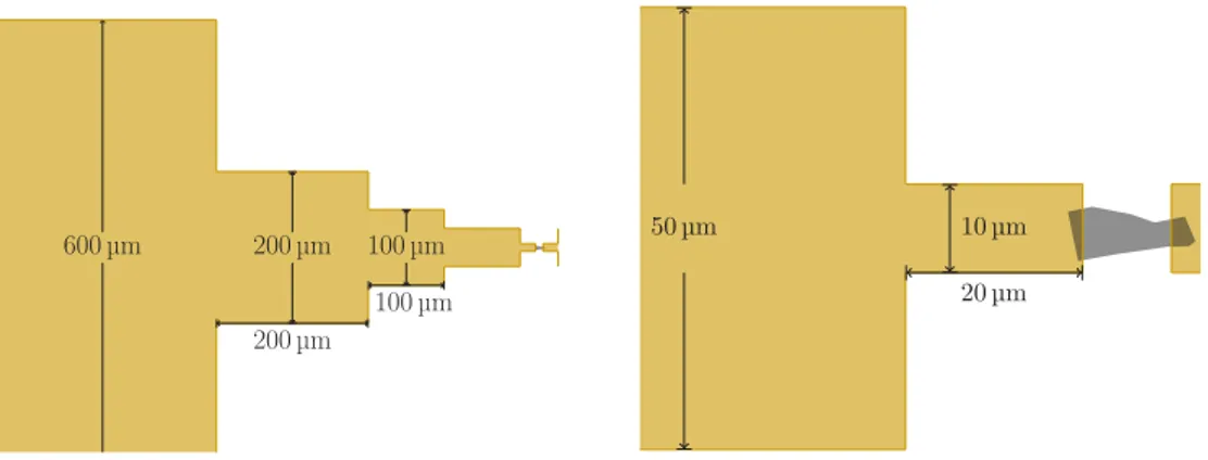
This is a realization of the system in figure 3.2 (e), the top plate being our gold/graphene system and our larger back plate being the silicon bulk. Once a graphene flake has been isolated, the size of the obtained flake determines the dimensions of the distance between the two gold electrodes. The final sample design, subject to small changes due to processing, can be seen in figure 4.2.
14 CHAPTER 3. METHOD The STM used in this project was a JEOL JSPM-4500A which is a combined UHV STM and AFM. All experiments were performed in the base pressure of the machine at ≈10−8mbar. It is controlled with a RHK R9 SPM controller, that has a home made custom
python interface with a program to control the coarse motors as well as data acquisition. The sample holder for the system used, utilizes a rather large screw and clamp to fasten the sample to the sample holder. This clamp also acts as the electrode to the sample. However, due to background disturbances in the signal from these macroscopic pieces, the sample was glued to the sample holder using a UHV-compatible epoxy and connected to the bias lines with wire bonds and UHV silver epoxy. By doing this, the large clamp and screw was replaced by the very thin 25µm Au wire from the wire bonder. Such disturbances were not seen after this. The bias lines in this setup consists of two large gold pads on the sample holder, on each side of the sample. The back gate was connected by scratching on the silicon oxide and thereafter wire bonding directly on the exposed silicon bulk to the electrode on one side of the sample holder. The gold patch was connected by a wire bond to the other electrode on the opposite side of the sample holder and then using a silver epoxy, attached to the large gold pad. The tip that was used was a commercial Pt tip with bulk diameter of 500µm that had first been mechanically sharpened and then electrochemically etched. The tip radius of the tip was <20 nm.1 The system had a noise level in tunnelling under 10 pA
and the set point for tunnelling scans was between 50 pA to 100 pA with a bias of 0.1 V. The modulation for the capacitive scans was set such that the front gate had a 200 mV modulation and the back gate was then adjusted to a value so that it was close to zero far outside the gold, on top of the silicon. This was due to a bug in the output from the STM controller’s software interface to python, corrupting data that was negative. Without this bug cleaner data might have been obtained.
3.5
Coarse XY-stage
Before presenting the results a few remarks on the coarse stage are appropriate. Many of the problems in this project were due to the coarse stage and it’s electric motors. First of all, the coarse stage motors are very noisy causing the whole STM to vibrate when in operation, creating large amounts of disturbance in the signal. To work around this the line scan measurements were implemented in a python interface. A program was written that takes a small step in in the XY -plane with the coarse motors, pauses until the vibrations have stopped and then does the measurement and iterates this process. Although this eliminates most of the noise it also makes the scans very slow. For the box and intensity scans 100 measurement points were taken over 100 lines which had to be done overnight. Further, the coarse stage is not Cartesian as it rotates the stage rather than moving it parallel to the XY -axis. Therefore a local calibration could have been made yielding a locally, fairly accurate Cartesian map. However since the interest of the project was precisely scan over large areas, this was not deemed useful. Additionally, the motors were non-deterministic. Running the motors with a for-loop, iterating a specific times and voltage, yielded different results in actual movement, sometimes for each of the iterations. Some iterations it would not move at all, others it would move the equivalent of many ”normal” iterations. These issues were minimized to the capacity of the lab by disassembling the entire STM and using UHV compatible lubricant on the inside and motor oil on the external motors, but they were still problematic. The only information available for these steps are how long the motors were fed with a voltage and how large that voltage was. Both parameters have consistently been constant during each measurement so the steps should be equidistant, but as the above
3.5. COARSE XY-STAGE 15 discussion implies, only the trends (averages over many steps), are somewhat reliable. Due to these issues, together with the fact that the methods developed here are mainly intended to be used on a different STM utilizing a piezo-coarse stage that presumably wont have these issues, a calibration was not attempted. The capacitive line scans, for example, does not have a calibrated X-axis so the distances the tip traverses is unknown, however the optical access microscope confirmed that it had traversed the line intended. Due to this the majority of the line scans also had to be completely discarded. An indication of the distance can be the width of patch the tip traversed, but using the data that you are trying to measure to calibrate your data, is, let’s say not rigorous. Therefore the capacitive graphs in this section will lack a proper measure on some axes, sometimes I denote it as simply distance and others as steps. So for all of the capacitive measurements and graphs, the data can be qualitatively interpreted and has been confirmed by optical access, see for example 4.1.
Chapter 4
Results
First, the final design chosen is presented.
Secondly, some line scans, reproducing Li et al’s results. These are taken as confirmation that the implementation is working similarly as theirs. In a similar way a box-scan mode has been performed, putting many of these lines together and making a intensity plot from the data.1 Although the box scan goes somewhat outside the scope of the objective of the
project, it does support the physics of the method.
Last but not least, atomic resolution images on a graphene are presented after successful landing using the the aforementioned method.
Figure 4.1: Tip and sample inside STM. Silver epoxy for wire bonding on the largest pad can be seen in the background.
4.1
Final Sample design
The final sample design can be seen in figure 4.2 and figure 4.3. Images of a fabricated sample can be seen in the optical microscope image in figure 4.4 as well as in a AFM image in figure 4.5.
1This was mostly to keep busy during a extended period of waiting for a new sample after wire-bond
short-circuited one sample.
18 CHAPTER 4. RESULTS
y
x
1000
µm
1000
µm
500
µm
600
µm
Figure 4.2: Final design used. The substrate is a silicon oxide wafer (not shown). The last patches cannot be seen in this image. The largest gold pad on the sample is 1 mm2. Each
subsequent patch has a smaller width as illustrated in the subsequent images.
1000µm 1000µm 600µm 200µm 200µm 100µm 100µm 1000µm 1000µm 600µm 200µm 200µm 100µm 50µm 10µm 20µm 100µm
Figure 4.3: (a) Zoom in on the sample from figure 4.2. (b) Further zoom in of same device showing the last gold patches and the graphene.
By going across the patches (P1P2in Figure 3.4) we have obtained data of the capacitive
pickup and how it increases as we pass the tip over the sample. Some such lines can be seen in images 4.6. These curves are similar what is expected, the lock-in amplitude increasing as the STM tip moves onto the gold, and then decreasing as it moves off it again. The objective is to land on the graphene, that is facilitated by the maxima in figure 4.6 (a). Precise positions of edges, are not as important for this implementation. Perhaps if landing close to the actual edge of the conductor is important, this would be of more relevance.
4.2
Line and box scans
Figure 4.6 demonstrates a linescan as in Li’s paper. Note that the current is quite noisy due to mechanical vibrations and friction in the system. This noise obviously also gets amplified in the numerical derivative. For example there is a plateau in the current in the blue and green lines close to the end. This is due to friction, causing the STM-tip to stand still in spite of the motors pushing it, effectively charging a potential energy into a spring-like system. Once the potential energy overcomes the friction, all the stored energy is released
4.2. LINE AND BOX SCANS 19
Figure 4.4: (a) Monochromatic optical microscope image of one of the samples. The dark parts are silicon oxide and the bright parts are gold. PMMA residues can be seen around sample as well as markers from the EBL processing. Unfortunately this sample was short circuited but a sample with same design was used. (b) Zoom in of the last patches of gold. The graphene can only very faintly be seen in the optical microscope.
Figure 4.5: (a) AFM image of the sample above with the electrodes on top and bottom, as well as a patch of exfoliated HOPG or multilayer graphene on the left side, connecting the electrodes. The gold electrodes are approximately 60 nm thick. The line profiles in (b) indicate that the graphene patch in image (a) has a step height in the order of 6 nm indicating multiple layers of graphene. Note that the graphene is rather thick, and thus it’s profile is visible ”through” the gold due to raising it’s profile. Raman spectroscopy confirmed presence of both multiple layers as single layer graphene.
and it moves a large distance very quickly, as indicated by the near vertical lines. This description was corroborated by observation many times and even recorded and confirmed with the optical access microscope during the course of the project.
Implemented in python by simply adding many capacitive line scans (x-direction) side-by-side with perpendicular (y-direction) coarse motor steps in between, the box scans are presented in 4.7 and 4.8. The coarse motor issues mentioned in the previous chapter, makes it very challenging to know where the scan box is actually going to be. Due to this the
20 CHAPTER 4. RESULTS
Distance
0.0
0.2
0.4
0.6
0.8
1.0
No
rm
ali
ze
d
LIA
,
I/
I
maxDistance
10
8
6
4
2
0
2
4
6
Derivative, arbitrary units
Figure 4.6: (a) The lock-in amplitude plotted against distance. The size of the gold pad that the STM tip passes in each of these lines is 1 mm. However, due to the motors on the coarse stage, the actual distance for each step is unknown. (b) Numerical derivatives of the curves in (a).
images in this section are a bit misaligned with the samples but they still support the physics: the current is larger when the tip is over the conductor and lower when it is over the insulator.
There are many ways to visualize box scans of this type, one can for example plot the data with an intensity plot or a 3D-plot. Different methods have their pro’s and con’s, here both aforementioned methods are included. Note however, the Z-axis in the (pseudo-)3D plot is not actually a spatial axis as normally is the case in SPM, but simply the increase in the current.
4.2. LINE AND BOX SCANS 21 50 100 steps in x 50 100 steps in y 0 4 8 12 16 20 24 28 32 36 pA
Figure 4.7: Intensity plot of a box scan. One box scan with 100 measurement points in the x and y direction. Z is the current as measured by the lock-in amplifier. Overlay image indicates approximate electrode placement and scan region on sample. The last gold pad is approximately 13µm to 15 µm.
100 steps in x
100 Steps in y
pA
16
40
100 steps in x
100 Steps in y
pA
16
40
100 steps in x
100 Steps in y
pA
16
40
16
26
36
pA
Figure 4.8: A different visualization of the same data as in 4.7. The images are rotated 30 degrees compared to eachother.
22 CHAPTER 4. RESULTS
4.3
Successful landing on graphene
The method developed during the course of this project has enabled a landing on graphene on silicon, supported here by STM images. First, for comparison, one image on evaporated gold is included in figure 4.9 as a reference for what it would look like if the landing was actually on gold and not graphene.
Figure 4.9: (a) Typical STM image on evaporated gold. The “blobby” features is what is to be expected when the gold is evaporated and not crystaline. Image is from final, 10µm wide gold pad on sample. (b) Surface profile of same image.
In figure 4.10 we see a large scan on something that looks very different from 4.9. The corrugation indicates it might be graphene/HOPG on silicon.
Figure 4.10: (a) STM image of graphene on silicon oxide. (b) Surface profile from STM image of graphene on silicon. Note that the Z-range is almost one order of magnitude smaller than that on the gold, which is to be expected [26].
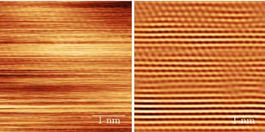
4.3. SUCCESSFUL LANDING ON GRAPHENE 23 Figure 4.11 and 4.12 are a zoom in on one of regions of figure 4.10. The images reported are some of many scans with more or less pronounced hexagonal lattice structure. On some of the images the graphite “three-by-six” structure is also seen [26], which is to be expected as our exfoliated graphene is expected to have some single layer regions and many multilayer regions.
Figure 4.11: Atomic resolution STM images on a flake of exfoliated HOPG/graphene ap-proached with the method developed in this project. (a) Raw STM image. (b) Same image after a FFT filter.
Figure 4.12: Atomic resolution STM images on a flake of exfoliated HOPG/graphene ap-proached with the method developed in this project. (a) Raw STM image. (b) Same image after a FFT filter.
The method has been successful in identifying edges of gold and approaching gold patches with widths from 1 mm to the last 10µm wide gold patch. Further it has successfully approached the graphene patch that is smaller than the last gold patch.
Chapter 5
Summary and Conclusions
The project was successful and a method for landing on a small patch of a conductor on an insulating substrate was implemented.
The first months in this project was spent trying to implement a method with physical guides but many issues stifled our progress. Most of them were related to the close sighted-ness of a STM, leading to time consuming approaches and stitching of 2µm images when trying to navigate in mm ranges. The main benefit of the method implemented is definitely that the capacitive navigation is easily implemented over these distances thanks to being a non-contact modality. Avoiding tunnelling means one can move across the surface at much higher speeds than the scan speed of a normal STM in feedback. These distances are the order of most STM setups total sample size so one can utilize this method over the entire sample.
Another difficulty during the project was finding literature that discussed capacitance in STM outside the dominating scope of finding doping profiles in insulators. Some early work has been done, most notably by Sakai and Kurokawa, and without a doubt some work has been overlooked in the process. However, to this day one of the major grievances with STMs is that they are time consuming, especially in the approach. The fact that a major commercial company such as RHK only recently is looking into an implementation of capacitance for their approach, indicates that these concepts may be somewhat overlooked overall. Other groups at Leiden Institute of Physics are implementing a capacitive fast approach, set for publication imminently, highlighting the topics relevance today.
As in any project, this is unfortunately not a conclusive end. Many things remain to be studied, bias modulation frequency, material influences on the capacitive signal are all interesting topics. Customizing the tip and the sample promise some of the most intriguing possibilities. For future implementations, longer gold patches or a thinner tip would be recommended as the STM-tip has a bulk size of a couple of hundred µm. Thus the bulk tip radius is on the order of the length of the last patches. This was not an issue for the implementation but perhaps even cleaner signals can be found using a system where the patches are much longer than the tip radius. A sample design where the whole sample is covered in gold, except a thin stripe along the middle where the graphene flake is situated, is in retrospect an interesting candidate. But as always, in any project, time frames are a real parameter.
Bibliography
[1] G. Binnig and H. Rohrer Scanning Tunneling Microscopy, Surf. Sci., 126, pp. 236-244, (1981).
[2] C. J. Chen Introduction to Scanning Tunneling Microscopy, Second Edition, Chapter 13: Tip treatment, Oxford Scholarship Online (2007)
[3] K. S. Novoselov et al. Electric Field Effect in Atomically Thin Carbon Films, Science, 306, (2007).
[4] Li et al. Transfer of Large-Area Graphene Films for High-Performance Transparent Conductive Electrodes, Nano Let. 9, 12, pp. 4359-4363 (2009).
[5] G. Nanda et al. Defect Control and n-doping of Encapsulated Graphene by Helium-Ion-Beam Irradiation, Nano Lett. 15, 4006-4012 (2015).
[6] C. J. Chen Introduction to Scanning Tunneling Microscopy, Second Edition , Oxford Scholarship Online (2007), retrieved on 2015-12-02
[7] Bharat Bhushan Nanotribology and Nanomechanics, Measurement Techniques and Nanomechanics, Volume I, Springer-Verlag, Berlin, Germany (2011)
[8] S. Kalinin and Alexei Gruverman Scanning Probe Micropscopy, Electrical and Elec-tromechanical Phenomena at the Nanoscale, Volume II, Springer Science+Business Media, LLC, New York, USA (2007)
[9] C. D. Bugg and P. J. King, Scanning capacitance microscopy, J. Phys. E: Sci. Instrum. 21, pp. 147-151 (1988).
[10] J. R. Matey and J. Blanc, Scanning capacitance microscopy, J. Appl. Phys. 57, 5 (1985).
[11] C. C. Williams et al. Scanning capacitance microscopy on a 25 nm scale, Appl. Phys. Let. 55, 203 (1989)
[12] A. Shik and H. E. Ruda, Theoretical analysis of scanning capacitance microscopy, Phys. Rev. B 67, 235309 (2003).
[13] S. Anand Another dimension in device characterization, IEEE Circuts and Devices Magazine 16, 2, pp. 12-18 (2000)
[14] V. V. Zavyalov, J. S. McMurray, and C. C. Williams Journal of Applied Physics 85, 7774 (1999); doi: 10.1063/1.370584 Scanning capacitance microscope methodology for quantitative analysis of p-n junctions, Jour. of Appl. Phys., 85, 7774, (1999).
28 Bibliography [15] S. Kurokawa and A. Sakai, Gap dependence of the tip-sample capacitance, J. Appl.
Phys. 83, 7416 (1998).
[16] S. Kurokawa and A. Sakai, Tip Sample Capacitance in STM, Sci. Rep. RITU A 2, 44 (1997).
[17] S. Lanyi and M. Hruskovic, The resolution limit of scanning capacitance microscopes, J. Phys. D: Appl. Phys. 36, pp. 598-602 (2003)
[18] I. Ekvall et al. Preparation and characterization of electrochemically etched W tips for STM, Phys. Rev. B 10, pp. 11-18 (1999)
[19] T. Hagedorn et al. Refined tip preparation by electrochemical etching and ultrahigh vacuum treatment to obtain atomically sharp tips for scanning tunneling microscope and atomic force microscope, Rev. of Sci. Inst. 82, 113903 (2011)
[20] W. Paul et al. FIM tips in SPM: Apex orientation and temperature considerations onatom transfer and diffusion, Appl. Surf. Sci. 305, pp. 124-132 (2014)
[21] A. K. Geim and K. S. Novoselov The rise of graphene, Nature Materials, 6, (2007). [22] M. Katnelson Graphene: Carbon in Two Dimensions, Cambridge University Press,
New York, USA, (2012)
[23] A. H. Castro Neto et al. The electronic properties of graphene, Rev. of Mod. Physics, 81, (2009).
[24] G. Li et al. Self-navigation of a scanning tunneling microscope tip toward a micron-sized graphene sample, Rev. of Sci. Inst. 82, 073701 (2011).
[25] Alicja Bachmatiuk Graphene Fundamentals and Emergent Applications, First Edition, Chapter 5: Characterisation Techniques, Elsevier, Massachusetts, USA First edition 2013 (2007)
[26] E. Stolyarova et al. Proceedings of the National Academy of Sciences of the United States of America, 104, 22, pp. 9209-9212 (2007), National Acedemy of Sciences

![Figure 2.2: Graphenes electronic dispersion with a zoom in of one of the symmetry points (commonly K, K 0 in the Brillouin zone or dirac-points), from [23]](https://thumb-eu.123doks.com/thumbv2/5dokorg/5474829.142477/20.892.209.718.182.455/figure-graphenes-electronic-dispersion-symmetry-points-commonly-brillouin.webp)