Independent degree project
Gate driver solutions for high power density SMPS using Silicon Carbide MOSFETs
Farhan Akram
Thesis work for the degree of Master by research in Electronics
Main field of study: Power Electronics
Examiner: Göran Thungström
Supervisor: Kent Bertilsson
Semester, year: 04, 2021
Course code: EL036A/ D2791- 15.0 hp
quired for the advancement of gate drivers for high voltage SiC transis-tors. A drive circuit for a SiC MOSFET needs to be optimized in normal operation to give best efficiency and same drive circuit should secure the MOSFET under unsuitable conditions. To ensure the rapid switching of these advanced SiC MOSFETs, a gate driver capable of providing the high current capability is required. In this work, three different high-power-density, high-speed, and high-noise-immunity gate driver modules for 10 kV SiC MOSFET were built and optimized. Double-pulse test was devel-oped for the dynamic characterization of SiC MOSFETs and gate drivers. This setup provided clean measurements of DUT voltage and current un-der well-defined conditions and correlated to simulation results. De-signed gate drivers have thoroughly investigated to test and compare it with our future design. The influential parameters such as dV/dt, dI/dt, and gate driving capability of gate driver were adjusted according to the requirements. The short circuit protection test was performed to check the reliability of driver modules in worst conditions. Furthermore, a DC-DC converter was designed and tested with the advanced gate drivers. The driver modules were tested in designed converter under different load conditions and influential parameters were successfully demon-strated. The driver modules effectively helped in reducing the EMI and switching losses. These designed gate drivers and prototype converter provide all the attractive features and can be widely implemented in in-dustrial applications for energy efficient systems.
Keywords: SiC MOSFETs, Gate drivers, DC-DC converter, High power
Acknowledgements
I express my sincere gratitude to Prof. Dr. Kent Bertilsson for giving me the opportunity to work in his group for my Master program. Thank you for your support. I appreciate your efforts and patience in as a mentor. Thank you for being approachable and nice in providing moral support. I express my sincere gratitude for all that you have taught me.
I am grateful to Mats Wårdemark for giving me a chance to work on this project in close collaboration with POWERBOX AB. The completion of my master thesis would not have been possible without your guidance. I appreciate your immense knowledge, resilience, and support that you shared throughout my master’s program.
I am also thankful to Prof. Dr. Mietek Bakowski from RISE for actively collaborating together with the project. I greatly appreciate his support to find out the solution of the problems which we faced during this phase.
I am also thankful to Dr. Sobhi Barg, and Farhan Alam for their support and healthy conversations during my stay in the lab. Thanks to my classmate Ali Rezaee for his cheerful support during my stay in Sundsvall.
Beyond academic network, I like to thank my friends who have been my support system throughout my stay in Sweden. I dedicate my thesis to my sister and parents, immensely supportive and understanding, thank you for being my strength and for your unconditional love.
Acknowledgements ... iv
Table of Contents ... v
Terminology ... viii
Acronyms / Abbreviations ... viii
Mathematical notation ... viii
1 Introduction ... 1
1.1 Background and problem motivation ... 1
1.2 Overall aim ... 2
1.3 Concrete and variable goals ... 2
1.4 Scope ... 3
1.5 Outline ... 3
1.6 Contributions ... 4
2 Theory / Related work ... 5
2.1 SiC MOSFETs structure ... 5
2.1.1 Intrinsic resistance and capacitance in SiC structure .. 6
2.2 Silicon vs SiC MOSFETs ... 8
2.3 Important parameters of SiC MOSFETs ... 9
2.4 IV-Characteristics ... 9
2.5 SiC MOSFET Switching Characteristics ... 10
2.5.1 Definition of switching characteristics parameters ... 11
2.5.2 Turn-On Switching Characteristics... 11
2.5.3 Turn-Off Switching Characteristics ... 13
2.6 Influence of gate driver on SiC MOSFETs ... 13
2.6.1 Turn- On ... 14
2.6.2 Turn-Off ... 14
2.6.3 Driver strength (IG) ... 15
2.6.4 Propagation delay ... 16
2.6.5 Threshold Voltage and Source Inductance ... 17
2.6.6 Miller Effect and Gate Drive Impedance ... 18
2.8 Switching losses in MOSFET ... 23
2.9 Gate Driver for SiC MOSFETs ... 25
3 Methods ... 28
3.1 Double pulse test ... 28
3.2 Evaluation of Gate drivers ... 28
3.3 Evaluation of SiC MOSFETs with gate drivers ... 28
3.4 Simulation Models ... 29
3.5 Evaluation of drivers in DC-DC converter ... 29
4 Implementation ... 30
4.1 Gate driver ICs ... 30
4.1.1 Gate driver A: Texas Instruments Incorporated - Ucc27531 ... 31
4.1.2 Gate driver B: Infineon- 1ED020I12-F2 ... 32
4.1.3 Gate driver C: Analog Devices- ADuM4135 ... 32
4.2 Power supply design ... 33
4.3 The gate driver schematic and prototyping ... 34
4.4 Double-Pulse Test Setup Description ... 38
4.4.1 Load Inductor... 39
4.4.2 DC Capacitor bank ... 39
4.4.3 Bleeder resistor ... 40
4.4.4 The device board ... 41
4.5 Measurement of voltage and currents... 42
4.5.1 Oscilloscope selection ... 42
4.5.2 Voltage probe and current measurement ... 42
5 Results and discussion ... 43
5.1 DPT test results ... 43
5.2 Selection of SiC DUT ... 44
5.3 Silicon carbide Schottky Diodes(SBDs) ... 46
5.4 The dV/dt and dI/dt ... 49
5.5 Influence of gate resistance Rg ... 51
5.6 Gate driver results ... 54
5.7 The gate Current ... 55
5.8 DPT Switching losses ... 56
5.9 Propagation delay ... 57
5.10 Short circuit protection ... 59
5.11 Simulation verification ... 61
6 Prototype of 1kW SiC based Half- Bridge DC-DC converter ... 64
6.2.6 PCB layout ... 72
7 Experimental validation of gate drivers in prototype converter 75 7.1 Basic operation test ... 75
7.2 Gate drivers test in designed converter ... 79
7.2.1 Miller effect avoidance... 79
7.3 Gate drive modules tests ... 80
7.3.1 The gate current measurements in prototype ... 83
7.4 Switching loss comparison in SiC DC-DC converter ... 84
7.4.1 Switching loss estimation ... 84
8 Discussion ... 89 8.1 Social aspects ... 92 8.2 Ethical aspect ... 92 9 Conclusions ... 93 9.1 Future work ... 94 References ... 95
Appendix A: MATLAB Scripts ... 99
Switching losses calculations: ... 100
Appendix B: PWM generation in prototype converter ... 103
Terminology
Acronyms / Abbreviations
MOSFET Metal Oxide Semiconductor Field Transistor
WBG Wide Band Gap
Si Silicon
SiC Silicon Carbide
GaN Gallium nitrite
DUT Device under test
SMPS Switch mode power supplies
HS High side
LS Low side
PCB Printed circuit board
D Duty cycle
PWM Pulse width modulation
SBD Schottky barrier diode
DPT Double-Pulse Test
Mathematical notation
Symbol Description VGS Gate-to-source voltage VDS Drain-to-source voltage IDS Drain-to-source currentCGS Gate-to-source capacitance
CGD Gate-drain capacitance
1
Introduction
The consumer demand for wide-band gap Silicon carbide semiconduc-tors has been accelerated exponentially due to their superior material per-formance and high efficiency. The WBG industrial growth is expected to increase from current figure of 750 million € to 1812 million € at the end of 2025 [1] .
Figure 1 Silicon Carbide market growth between 2019-2025 (EURO Millions)
1.1
Background and problem motivation
SiC technology enabled electric vehicles to meet the design parameters required in high-power applications leading to better system perfor-mance and longer reliability. Global industries continuously make an ef-fort to enhance the performance of available SiC devices. An increasing number of SiC MOSFETs with voltage ratings between 600 V and 1700 V are hitting the market with decreasing Rds (on) and costs as well as suffi-cient reliability. We wanted to make better the performance of available SiC devices with suitable application and system environments. The sim-ple and traditional method for driving the MOSFET is the direct drive from the logic signal. Such method has a low current drive and slower transition with lower gate to source (VGS) magnitude. The microcontroller
protection features, low inductive paths, and optimized driving capabili-ties are required for higher frequency applications to minimize the overall losses [3].
1.2
Overall aim
The overall aim of this thesis is to develop and optimize the gate driver solutions for SiC MOSFETs for the transport and industrial applications. The gate driver solutions should address all the issues related to noise in the system, overvoltage, and short circuit protection features. The de-signed SiC gate driver should reduce the spikes and rigging under nor-mal and short circuit conditions to enable the dramatic increase in power density.
1.3
Concrete and variable goals
The work is emphasised on achieving high electrical efficiency from SiC switches and their gate drivers in advanced switch-mode-power-supplies (SMPS) to align it with commercial applications. The study-specific ob-jects were:
1. Developing and optimizing a gate driver solution for a SiC MOSFET for achieving high power density.
2. Comparing the influence of different gate drive modules on SiC switches
3. Evaluation of feasible and commercially available SiC MOSFETS and further characterization on double-pulse test setup.
4. Investigating the switching transitions of the SiC switches and gate drivers were thoroughly.
5. Building-up a prototype with DC-DC converter with advanced SiC switches and gate drivers.
6. Investigating the impact of latest gate drivers and SiC switches in DC-DC converters. In the end, SiC based DC-DC- DC-DC converter was optimized with suitable protection features.
7. Determining the electromagnetic interference (EMI) due to fast switch-ing transitions.
1.4
Scope
The work done in thesis led to promising results regarding the use of advanced gate drivers in power converters. The designed gate drivers address the critical challenges that arise in operating SiC MOSFETs at high voltage and frequencies. The designed driver modules effectively help in reducing the EMI and switching losses. The designed gate drivers offer an ultimate solution to the industry, which is thriving to attain energy efficient systems as per new EU regulations.
1.5
Outline
Chapter 2 provides a background overview of SiC MOSFETs, their basic structure, comparisons between Si and SiC MOSFETS, and IV character-istics. It also includes the switching characteristics and influence of gate drivers on SiC MOSFETs.
The potential applications of SiC transistors such as clamp inductive load, switching loses, and gate driver techniques are given in chapter 3. This chapter presents a general background of the SiC MOSFETs in the switch mode applications. The first section covers the theory related to analyse switching transients and calculate the power losses in the applications. While section two shows the background about SiC MOSFETs based half-bridge DC-DC converter and gate driver design approach.
Chapter 4 shows the implementation and design of the gate driver mod-ules, different stages of design, power supply design, PCB layout and the selection of gate driver IC. The chapter 5 explains the design for test ap-proach such as double pulse test description, measurement setup and methods.
signed parameters. Chapter 8 covers the experimental validation of pro-totype converter and presents the results of these gate drivers and SiCs. Multiple tests have been conducted on various configuration to success-fully demonstrate the functionality of prototype converter with these ad-vancements are shown.
1.6
Contributions
The project was conducted mainly at STC research centre, Sundsvall, Sweden, in active collaboration with industrial partners, PowerBox AB, Gnesta and RISE Acreo, Kista, which provided essential insights, useful resources, and access to the latest technologies. The project was funded by Swedish Energy Agency and PowerBox AB.
2
Theory / Related work
SiC MOSFETs are wide-band gap devices consisting better properties as compared to Si semiconductors. For example. SiC MOSFETs principally provide fast switching speed with low switching losses. The commercial SiC modules use simple and reliable wire bonding technology with wider energy bandgap. Such physical characteristics equip the devices with an improved overall efficiency by providing high critical breakdown field and thermal conductivity than their conventional counterparts [4] [5]. Due to the exceptional performance made possible by silicon carbide power devices, control electronics are required to operate in the same demanding conditions. The reduced switching power losses allow high frequency operation ultimately and reduce the overall system cost [6]. The fast switching is compulsory for avoiding long transients of the MOSFET ohmic region operation. In the on time, a positive gate drive voltage should be applied to keep the on-resistance as low as possible.
2.1
SiC MOSFETs structure
The SiC MOSFET works as a switch in such a way that the gate controls the current flowing from drain to source. In a typical SiC MOSFET structure, two opposite p-n junctions make source-to-body junction and drain-to-body junction. The junction blocks the voltage either from drain to source or source to drain as shown in Figure 2. The BJTs bipolar devices enhance the conduction between collector and emitter by injecting the minority carriers through their base terminals. While in the MOSFETs, gate terminal is gate-oxide insulated. However, the negative charges start accumulating on the gate terminal when a positive voltage with a reference to the source is applied to the gate terminal. Ultimately, a conduction channel forms between drain to source allowing the drain current to pass between the two terminals [7] [8]. SiC MOSFETs usually come in TO-247 and TO-247-4 packages. TO-247 has three terminals such as Gate (G), drain (D) and source (S). While TO-247-4 comes with an extra terminal to have a shorter path to the gate called kelvin source.
Figure 2 Internal structure of MOSFET 2.1.1 Intrinsic resistance and capacitance in SiC structure
The detailed n-channel SiC MOSFET structure showing its intrinsic re-sistances is shown in the Figure 3.
Figure 3 Intrinsic resistances present in the N channel MOSFET
The drain to source resistance RDS(on) of the SiC device is the sum of
pre-sent intrinsic resistances in the model as shown in the equation (1.1).
R
DS(ON) = RCS + RN + RCH+ RA + RFET+ RD+ RSUB+ RCD (1.1)
The intrinsic resistances are temperature-dependent, and capacitances are temperature-independent. This means that the conduction losses de-pend on the temperature while switching losses of the MOSFETs are ra-ther independent of temperature as switching speed relates to charging and discharging of the input capacitance (Ciss). However, the gate-to-
drain capacitance (CGD) and the gate-to-source capacitance (CGS) depend
on are voltage applied [31]. Input capacitance (Ciss) is the sum of CGS and
The equivalent circuit for the intrinsic capacitances in an n-channel MOSFET is shown in Figure 4.
Figure 4 Equivalent Intrinsic capacitance present in the N-channel SiC MOSFET
Output Capacitance (Coss) is equivalent to the sum of drain-to-source
ca-pacitance (CDS) and gate-to-drain capacitance (CGD) and influences the
res-onance of the circuit. Reverse transfer capacitance (Crss) is the gate to
drain capacitance (CGD) and often referred as Miller capacitance. Crss
af-fects the voltage rise and fall time during switching [11][10]. The Figure 5 below shows the nonlinear curves for input and output capacitance vs drain to source voltage in SiC MOSFET. It can be verified that the input capacitances CGS and CGD are heavily drain to source dependent [11].
Figure 5 SiC MOSFET Capacitance vs VDS curve
Ciss must be charged in order to drive the MOSFETs. Gate-drain
capaci-tance (CGD) also called as miller capacitance is nonlinear function of
time. However, SiC MOSFETs have emerged as a new technology, show-ing benefits surpassshow-ing those devices given their intrinsic material prop-erties. As comparison to Si based devices the SiC offers superior ad-vantages like wider energy bandgaps, higher critical electric fields with thinner blocking layers, higher electron saturation velocity, and higher thermal conductivity. The higher bandgaps result in much lower current leakages and higher temperatures [13]. While higher critical electric fields and higher doping concentrations helps to come up with a thinner block-ing layer. Higher electron saturation velocity gives rise to higher frequen-cies. While the improved thermal conductivity helps in heat dissipation, thus the devices can work on higher power densities. These characteris-tics are summarized in Figure 6. The material properties of SiC directly translate into system-level advantages over systems using Si devices, in-cluding reduced size, cost, and weight. Consequently, SiC MOSFETs are increasingly replacing Si power devices [12].
2.3
Important parameters of SiC MOSFETs
Although SiC MOSFETs exhibit the similar general switching behaviour like traditional silicon MOSFETs, there are many considerable design re-quirements associated with the device characteristics. Recently, many in-dustrial SiC MOSFETs offer great features including low RDS(on), very low
switching losses, threshold-free on state characteristics, fully controllable dV/dt, and commutation robust body diode. SiC MOSFETs are known for their lower losses by providing the faster rise and fall time. Previous stud-ies showed that these fast slew rates lead to problems such as electromag-netic interference (EMI) [15] [13]. Some SiC MOSFETS also come with kel-vin source pin which effectively reduces the parasitic inductance of the source lead of the power MOSFETs. Some important characteristics of widely available SiC MOSFETS are shown in the Table 1 taken from the data sheets of manufacturer.
Table 1 SiC MOSFET overview
2.4
IV-Characteristics
The gate-to-source voltage (VGS) greatly influences the drain-to-source
re-sistance RDS(on) of the MOSFET, and eventually the drain current (Id) as
seen in the Figure 7. The field effect of the gate is increased due to high gate-to-source voltage applied. Hence, the on-state resistance is inversely proportional to gate-to-source voltage VGS(ON).
A MOSFET lies in its ohmic region when VDS influences the drain current,
but only when drain-to-source voltages is low. In the active region of the MOSFET, ID is independent of drain-to source voltage and only depends
on the gate-to-source voltage. Cutoff region of the MOSFET is the last re-gion where all the drain current is blocked [8] [10].
Manufacturer Part-ID Vrated
(KV) RDS(on) (mΩ) ID (A) VGS (V) VGS(th) (V) Ciss (pF) Coss (pF) Qg (nC) Rg (Ω) ROHM SCT2080KE 1.2 80 40 -4V,+22V 2.8 2080 77 106 6.3 CREE CMF20120 1.2 80 42 5V,25V 3.2 1915 120 90.8 5 Little-Fu LSIC1120E0080 1.2 120 25 -6V, +22V 2.8 1700 82 92 0.85 Infineon IMZ120R045M1 1.2 45 52 -10V, +20V 3.5 1900 115 52 4 CREE C3M0075120K 1.2 75 30 -4V, +19V 2 1350 58 51 10.5
Figure 7 SiC MOSFET I-V characteristics
As the field effect from the gate terminal is not high enough to induce a conducting channel between drain and source because of low gate to source voltage, thus blocking the Id.
2.5
SiC MOSFET Switching Characteristics
The typical switching characteristics of SiC MOSFETs are similar to their traditional Si counterparts. A typical circuit application for SiC MOSFET is shown in the following Figure 8. The load is purely inductive thus rep-resented by Io.
2.5.1 Definition of switching characteristics parameters
The typical switching transients for the hard switching applications with important parameters are shown in the Figure 9. It shows the turn-off and turn-on transients with important switching times and derivatives pa-rameters.
Figure 9 SiC MSOFET switching parameters
Where td(on) and td(off) represent the delay, when the gate to source voltage
VGS reaches to 10% and 90% of its final value with respect to the drain to
source voltage. The tr and tf are the rise time and fall times for drain to source voltage, respectively. The t(on) exhibits the 10% of VGS to 90 % final
value of VDS.
2.5.2 Turn-On Switching Characteristics
The switching transients of the MOSFETs include turn-on event together in a hard switching typical application as shown in the figure below. Firstly, it is assumed that the MOSFET is in its off state and Io is free-wheeling in the Schottky barrier diode (SBD). The load is assumed to be purely inductive and MOSFET is supplied with a positive gate to source voltage, as a result the turn-on transient will initiate.
Figure 10 MOSFET turn-on transient
With the rise in gate to source voltage, the capacitance CGS will be charged
by the gate current through gate resistance Rg. By charging the gate ca-pacitance CGS of the MOSFET, the field effect from the gate induces a
con-ducting path from drain to source and drain current starts to rise. The Rds(on) will decrease as the VGS increases until it reaches the load current
(t2). At point t2, capacitance CGS is fully charged and VGS levels a point
called Miller plateau [7].
During this period, the gate to drain capacitance CGD is charged by gate
current IG and the drain to source voltage starts falling towards zero. At
the interval t3, the drain to source voltage only depends upon the on- state resistance Rds(on) and the period is known as ohmic region [10]. The gate voltage of the MOSFET continues to rise until reaching the final gate volt-age. In the real application, MOSFET turn-on transient includes the verse recovery of the diode present within the MOSFET. The reverse re-covery event occurs at the time t2 due to the reverse rere-covery current (Irr)
present at the diode turn-off transition. Increase in the drain current due to Irr leads to a slight bump in the gate voltage (trr). Thus, the turn-on
2.5.3 Turn-Off Switching Characteristics
In the turn-on transition, the freewheeling diode is reversed biased when the load current I0 is flowing through the MOSFET. Now if the gate
volt-age (VGS) is pulled down to zero or negative level, the turn-off transient
will begin. The turning off event will involve exact same transition in re-verse order. The ideal switching behavior for turn-off is shown in the Fig-ure 11.
Figure 11 MOSFET turn-off transient
The actual turn-off switching events often show considerable overshoots in the voltage and currents at the time when VGS crosses the miller plateau
(t3) as shown in chapter 5.4. This effect happens due to stray inductance Ls resonance in the circuit causing the high dI/dt and overshoot in drain to source VDS. Such overshoots in current and voltage significantly
influ-ence the turn-off switching losses [3].
2.6
Influence of gate driver on SiC MOSFETs
Gate driver works as a power amplifier which can convert the low input power from the microcontroller to high current drive output. The SiC MOSFETs offer a lower transconductance than Si MOSFETs with almost same VGS, and thus the channel resistance decreases significantly with
VGS. It is recommended to maximize the VGS to a suitable value for
mini-mizing the conduction losses. However, as seen in the previous studies, SiC transistors demand a rapid transition in gate voltage without signifi-cant ringing and overshoots [13]. In comparison to conventional IGBT’s
current to the MOSFET rapidly. To drive advanced SiC devices on target requirements, the gate driver must perform turn-on and turn-off transi-tion safely.
2.6.1 Turn- On
The path of the source current of SiC MOSFET is shown in the Figure 12. The turn-on transition needs a large peak to peak current, efficient to charge the SiC internal gate capacitance and fast enough for minimizing the switching loss [17] [15]. The entire turn−on event occurs within ap-proximately few ns for a full VGS swing when ΔVGS = 15 V and calculated
CISS = CGS + CGD = 1000 pF, yielding a required peak current IG =1.5 A,
ac-cording to the following equation:
I G
=
(𝐶𝐺𝑆 +𝐶𝐺𝐷 ) . ∆𝑉𝐺𝑆
∆𝑡
(1.2)
Figure 12 SiC MOSFET source current 2.6.2 Turn-Off
Turn-off transition occurs in reverse order exactly of turn-on state as men-tioned in previous section 2.6.1. Gate drive circuit sinks a large amount of
the peak current which ultimately discharges the CGD and CGS capacitance
of the SiC MOSFET as fast as possible. Moreover, the gate driver imped-ance during turn-off should be minimum to hold the MOSFET gate low [16]. It can be problematic due to the low threshold voltage (Vth)
associ-ated with the SiC MOSFETs. It is compulsory that the SiC gate being pulled below ground and the capability of the sink current should be higher than the source current capability [19]. The flow of IGsink is
high-lighted in the Figure 13.
Figure 13 SiC MOSFET sink current 2.6.3 Driver strength (IG)
The gate current or drive strength controls how fast the device’s input capacitors charge and discharge. When the gate current increases, the switching losses decreases and vice versa. The required gate-drive strength depends on gate charge of the SiC MOSFET (Qg) as shown in Figure 14, gate current is calculated as in a time of ton is calculated as:
𝐼
𝐺 = 𝑄𝐺
𝑡𝑜𝑛 (1.3)
This current is the average current required to turn the device fully on. The region of interest, however, is the Miller plateau region, where the gate voltage is constant during the switching transient [16].
Figure 14 Gate capacitances of SiC devices 2.6.4 Propagation delay
Another important part in gate driver technique is to minimize the losses due to dead time and propagation delay. Higher frequency also means higher switching losses, having a higher propagation delay or dead time means that current circulating through the diodes in the loops and result-ing in more losses overall. Propagation delay is one of the key parameters of a gate driver that can affect the losses and safety of high-frequency sys-tems. Propagation delay is defined as the time delay from 50% of the in-put to 50% of the outin-put, as shown in Figure 15.
Figure 15 Pulse with distortion
This delay affects the timing of the switching between devices, which is critical in high-frequency applications where the dead time is necessary so that two devices do not turn on at the same time, which would cause
shoot-through and reduced efficiency [7]. If the dead time is smaller than the propagation delay, then both devices will turn on at the same time.
2.6.5 Threshold Voltage and Source Inductance
One of the most critical challenge faced by the designers of SiC MOSFETs is to control the gate threshold voltage. Early SiC MOSFETs had problems with threshold stability. The threshold shifts due to soaking at a bias con-dition. The continuous operation with a negative and positive gate bias at an elevated temperature usually results into a threshold shift [4]. These problems, however, have been resolved in the latest generations of SiC MOSFETs [17]. The threshold voltage is a compromise by design between noise immunity and RDS(on). The temperature dependence is nonlinear, so
the specified threshold is generally close to 2 V at 175 °C [11]. These prop-erties make the SiC transistors more sensitive to unintentional turn-on. To overcome this issue, a negative voltage at gate is often necessary to confirm a safer turn-off transition. The SiC transistor usually does not show a flatter Miller plateau but manifest a fine transition between the regions of the ohmic to saturation transition. Thus, it is recommended to have a higher voltage for gate around 18-20V [21] [3] [18].
It is highly suitable to use a negative gate voltage with the SiC MOSFETs in the high frequency switch mode power supplies. The gate to source voltage is designed below ground level to keep the device OFF when there is no active switching. The major reasons for using negative voltage are source inductance and gate drive impedance. Source inductance is the inductance introduced by the output current loop and gate driver current loop [15]. The gate drive voltage combined with the source inductance present in the loop have a significant effect on the higher frequency ap-plications under the load. This is due to the source lead inductance which couples the output switching current back to the gate drive and ulti-mately slow the gate drive. Gate drive impedance is important so that the gate driver provides a lower impedance path in off-state other than the on-state drive on the opposing transistor. This can limit the Miller effect and cross conduction losses in the bridge configuration [13]. Thus, a gate driver with a negative voltage option plays an important role in reducing the cross-conduction losses. The detail study and effects of the negative voltage will be presented in chapter 7.2.1.
current is pushed towards the gate by Miller capacitance CGD of the
com-plementary switch. A spike in VGS commonly appears due to the high
dV/dt by the Miller current. In case when VGS exceeds the threshold
volt-age due to the rapid negative slew rate, a shoot through in the bridge can occur as shown in the Figure 16. This is more common in the low thresh-old voltage power transistors specially SiC MOSFETs [18] [23] [24].
Figure 16 Miller effect seen in bridge configurations
In general, duality glitch phenomenon usually occurs due to the negative or positive dV/dt on the switching nodes resulting in the flow of IGD
through the capacitance CGD. The rapid change dV/dt induces higher
trumped-up gate voltage causing a shoot through in phase leg. Addition-ally, some of the current flowing through the CGD flows out through the
gate terminal and the gate driver sink resistance produces a spike in the gate voltage.
Figure 17 Parasitic turn-on in bridge configurations
This can drive the upper device back into conduction and can cause a short through. A typical illustration causing the spike is depicted in the Figure 17. There are different solutions to overcome this issue during the transistor turn-off transition. In general, limitation of gate loop and com-mon source inductances can minimize this false turn on phenomenon as explained in section 7.2.1. A small capacitor between the gate and source can be another option but will cause high losses overall and significant efficiency decrement. Moreover, selecting a gate driver with negative gate voltage option and low pull-down impedance path proves a significant improvement in the Miller avoidance [20]. One of the solutions is to choose a correct gate resistor ratio which can be 2:1 or 4:1. The reduction of Rg-off solves the issue to some extent. However, a smaller Rg-off might lead to extremely faster switching and very high stress on the transistor by generating the higher dV/dt. The higher dV/dt effect can be also lim-ited by choosing a higher gate resistor for the transition.
Figure 18 Active Miller clamp function in gate driver IC's
The other solution is more practical by adding the external pull down MOSFET to the gate which can bypass the Miller current during the turn-off. This solution is called active Miller clamp. The Miller clamp contains an extra MOSFET within the gate driver circuit as shown in Figure 18. This clamp circuit is controlled by the gate driver IC. The bypass MOSFET is normally ON when the gate to source voltage of M1 is reduced to the threshold voltage. This method is more practical as this will not affect ei-ther the switching time or dV/dt.
2.7
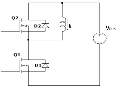
Clamped inductive load in MOSFET switching
In power electronics different topologies can be derived from a circuit consisting of two switches connected in series or parallel. The switches Q1 and Q2 can be used or replaced with internal body didoes D1 and D2 depending on the application requirements.
This structure is implemented in many converter applications such as boost and half-bridges and is called as H-bridge circuit. Multiple copies of the H-bridges can be used to form a 3-phase inverter or full-bridge dc-dc converter. Here, blocking is required inside orientation, and diode con-duction in the other direction is necessary for the proper operation. This operation can be obtained by activating or deactivating the switches, and this method is called as ‘synchronous switching’. Switch mode power supplies cast an inductive effect to the switching node (VSW) between the
two switches. This node can be further connected to an inductor forming a clamped inductive load. This specific set of the system has unique sys-tem dynamics. During the Q2, inductive load charges the inductor from the one side. While in the Q1 turn-on state, the inductor will be charged in the opposite manner.
Figure 19 H-bridge configuration in power electronics
In an ideal case where the load is purely inductive, the DC voltage Vbus is
applied to the load L, Q1 turns on and the inductor current will start to increase as given in equation 1.3. Q1 turns off and IL freewheels though
the diode VD1. Here, the IL starts to reduce slowly.
I
L
= 𝑉
𝐷𝐶 𝑡1𝐿
(1.4)
At the turn-off transition, the inductor adds the voltage of the output point node though the high side freewheeling diode. The current at this point is the full inductor current, and only starts to decrease when the diode is in the forward-biased condition. The voltage and current across the MOSFET terminals rise to VBUS and IL. At turn-on transition, this
pro-cess is reversed, the current from 0 to IL, while at voltage at VBUS, the
cur-rent reaches to IL and the voltage decreases. This is called ‘hard
switch-ing’ and usually involves the high peak power. There are other tech-niques to reduce the voltage or current stress across the switch which are called zero current switching (ZCS) and zero voltage switching (ZVS) [22].
Figure 20 Clamped inductive load example circuit, with optional synchronous MOSFET Q2
The clamped inductive load can be further explored by replacing the the-oretical switches with the real components as mentioned in the section 4.4. For such experiment, a MOSFET can be considered with an inductive load in the hard switching application. The idealized waveforms with clamped inductive load are shown in Figure 21.
The hard switching event with a clamped inductive load can be described in various phases, it begins with the VGS, changing from zero or negative
state to Vth. After VGS reaching the threshold limit, the MOSFET starts to
conduct current. The current starts to follow through the drain to source and drain to source voltage at this point remains constant. If the MOSFET drain current ID is less than the inductor total current, remaining inductor
current will have an additional path through the diode which is parallel to the load inductor. The drain voltage at this point is the voltage drop across the diode and remains above the Vbus. The gate to source voltage
will continue increasing until the drain current is equal to the inductor current [21]. As the drain current crosses inductor current, this makes the diode to come in reverse biased condition and drain voltage starts falling and MOSFET is in completely on-state.
Figure 21 Ideal MOSFET switching waveforms for a clamped-inductive load turn-on
It is important to note that the clamped-inductive switching configuration develops several peak conditions during switching that do not exist to the same extent in other common configurations. The clamped-inductive load guarantees that the MOSFET will experience maximum di/dt, dV/dt, and instantaneous power in a single controlled switching event [8]. While several performance maximums will occur, the system will constrain peak MOSFET drain currents, and the total energy dissipated is a function of the switching speed.
2.8
Switching losses in MOSFET
Conduction losses and the switching losses are amongst the major losses in half bridge configuration in MOSFET. The conduction losses occur due to on-state resistance of the power MOSFET. The drain to source voltage across the MOSFET is not zero due to the static conduction losses.
Pcond = 𝐼𝑑𝑟𝑚𝑠2× Rds𝑂𝑁 (1.5)
Where the ID is drain current through the switch. The RDS-ON is the on-state
parasitic resistance of the MOSFET. The ideal switching waveform is shown in the Figure 22.At lower frequencies, static conduction losses are more dominating and can be averaged over whole period.
Figure 22 Power transistor losses due to switching times and RDS(on)
𝐼𝑑𝑟𝑚𝑠 = √𝐷 (
𝐼𝑑𝑚𝑖𝑛+𝐼𝑑𝑚𝑎𝑥
2 ) (1.6)
Where Idrms is the RMS current through the switch and D is the duty cycle.
The switching losses can be divided in the rise and fall times for the MOSFET as mentioned in equation 1.6. The switch losses during rise time can be defined as:
Pr = 1 𝑇∫ 𝑉𝐷𝑆 𝑡𝑟 0 𝐼𝑑 𝑑𝑡 = 1 𝑇∫ 𝑉𝐼𝑁 𝑡𝑟 0 𝐼𝑑𝑚𝑖𝑛 (1 − 𝑡 𝑡𝑟 ) 𝑑𝑡 = 𝑉𝐼𝑁 .𝐼𝑑𝑚𝑖𝑛 𝑡𝑟 6𝑇 (1.7)
Where Vin is the input voltage and tr and tf are rise and fall times,
respectively.
The switch losses during on transition:
P f = 1 𝑇∫ 𝑉𝐷𝑆 𝑡𝑓 0 𝐼𝑑 𝑑𝑡 = 1 𝑇∫ 𝑉𝐼𝑁 𝑡𝑓 0 𝐼𝐷𝑚𝑎𝑥(1 − 𝑡 𝑡𝑟 ) 𝑑𝑡 = 𝑉𝐼𝑁 .𝐼𝐷 𝑚𝑎𝑥 . 𝑡𝑓 6𝑇 (1.8)
The gate charge losses can be defined as:
P
G = (𝑄𝑔−𝐻 + 𝑄𝑔−𝐿) . 𝑉𝑔𝑠 .𝑓𝑠𝑤 (1.9)
P
Where the Qg-H and Cg-H are the MOSFET gate electric charge, charge
capacity and fsw is the switching frequency.
Dead time losses can be defined as:
PD = 𝑉𝐷𝐷 . 𝐼𝐷 . (𝑡𝐷𝑟 + 𝑡𝐷𝑓) . 𝑓𝑠𝑤 (1.11)
Where the tDr, tDf are the rising and falling dead times and VDD is the diode
forward voltage of the lower MOSFET.
The turn-on and off energies can be calculated as:
𝐸𝑜𝑛 = ∫ 𝑉𝑑𝑠. 𝐼𝑑(𝑡)𝑑𝑡 𝑡𝑜𝑛 0 (1.12) 𝐸𝑜𝑓𝑓 = ∫ 𝑉𝑑𝑠. 𝐼𝑑(𝑡)𝑑𝑡 𝑡𝑜𝑓𝑓 0
(1.13) 𝑃𝑆𝑊= (𝐸𝑜𝑛+ 𝐸𝑜𝑓𝑓) × 𝑓𝑆𝑊
(1.14)
The overall switch losses are the sum of losses during all and can be specified as
Ptot = Pcond
+
Pr+
Pf+
PG+
PD (1.15)2.9
Gate Driver for SiC MOSFETs
A gate driver is the last and crucial stage of circuitry where the control logic determines different state of the MOSFET through the gate of the MOSFET. A simple microcontroller is only able to deliver somewhere 5V and few milliamps where these SiC devices need higher current to switch 15-20V at gate terminal to minimize the switching losses. Where tradi-tional drivers give low output drive and big latency in the switching pat-terns. As performing at elevated voltages and current levels require ad-ditional considerations like protection and isolation. The answer is to go with faster and more reliable design approach in the drivers.
A simple gate drive circuit can be built out of discrete components to drive a power MOSFET. Two simple BJTs or MOSFETs forming a totem pole or push-pull configuration can increase the drive strength as shown
More advanced gate driver type is the current source gate drivers which offers another solution for driving the power MOSFETs. The current source gate drivers use a charged inductor as a primary current source to charge and discharge the gate capacitances of the MOSFET as shown in the Figure 23(b). The current mode drivers offer two basic modes for op-eration which depend on the current stored in the drive inductor and the required energy to drive the MOSFET. The inductor requires the charging before turn-on and full discharging before the turn-off transition which increase the propagation delay from input to output. This solution is pre-sented in previous studies where it provides good current drive for the Miller plateau using the same energy stored in gate capacitances but re-sults in increased control latency and needs a more complex design ap-proach [25].
The gate driver connection to the MOSFET is another important design parameter [26]. The simplest method is a direct connection from gate driver output to the gate terminal of MOSFET. The latest gate driver ICs in the market can provide the high gate current thus require a modifica-tion before the gate of the power MOSFET as shown in the Figure 24(a). A gate resistance Rg can be added next to the gate driver IC output to reduce the output current. By removing the current limiting resistance, gate current is only limited by the internal gate resistance of the power
MOSFET or gate driver. The Rg adjustment requires an additional verifi-cation that the gate driver should provide sufficient but not excessive drive. The excessive drive can result in maximum dV/dt and overshoots in the drain to source voltage [20]. These overshoots can cause excessive stress to the power MOSFET. Fundamentally, the overall performance of the system is heavily gate driver dependent.
Figure 24 The gate driver current limiting solutions (a) turn-on (b) turn-off
Some gate driver IC’s in the market only provide the single output chan-nel instead of split outputs for turn-on and turn-off. For this approach, a diode in parallel with the separate pull-down resistor can be imple-mented in the design. This method can provide the different drive strength for turn-on and turn-off transition as shown in the Figure 24(b). The additional path provided by diode is used to short circuit the re-sistance for turn-off transition creating a lower impedance path for the current. Such solutions will result in higher noise immunity but will cast more complexity to the design and increase the overall cost [18].
3.1
Double pulse test
To match the concrete and verifiable goals for the project a double pulse test (DPT) setup is designed. The DPT tester demonstrates the gate driver driving the SiC MOSFETs and effects related to switching performances. The setup is designed to test different SiC MOSFETs, SiC Schottky barrier diodes, and different gate driver circuits. Wide band gap devices espe-cially SiC MOSFETs need prudent testing design. For example, circuit lay-out with minimum parasitics in the design is required for the accurate transients measurements. Further design layout is mentioned in the chap-ter 4.4.
3.2
Evaluation of Gate drivers
The SMD components on larger printed circuit board result in big current loops in the design influencing the driving performance of the gate driver. The commercial gate driver ICs come in small PG-DSO package with several performance benefits. Thus, it is always best to choose a com-mercial gate driver IC. Thus, four different gate drivers with superior per-formances are selected and optimized with decoupling capacitors and suitable power supply. The focus here is to design a gate driver in close proximity to the SiC MOSFET to minimize the inductance produced by long current paths [18]. The various gate drivers, their specifications and design are mentioned in 4.1.
3.3
Evaluation of SiC MOSFETs with gate drivers
One of the goals of the project is to investigate the SiC MOSFETs perfor-mances and integrate these devices into the required application. SiC MOSFETs in the market need to be investigated by datasheets and the result obtained from the DPT. The optimal target is to choose a device which offers balance between fast and clean waveforms. SiC MOSFET
needs to be compared with the same gate driver to observe the perfor-mances of both devices as mentioned in the section 5.2.
3.4
Simulation Models
A double pulse test simulation circuit is modeled in the LTSPICE to check the reliability of the gate drivers and SiC MOSFETs and results are com-pared between DPT and simulation. The common parasitics such as PCB parasitics and common source inductances are added in the simulation software. Some SiC MOSFETs manufacturers provide the spice models for their devices, thus these models are further investigated in the simu-lation circuit as described in the section 5.11.
3.5
Evaluation of drivers in DC-DC converter
After obtaining the evaluation of the drive circuits in DPT, a DC-DC con-verter in phase leg configuration is built. The performances of drive cir-cuit can be different in the DPT and converter due to rapid change in cur-rents and voltages in the converter. As the SiC MOSFETs usually operate at very high voltage and current levels, the driver actual performance is monitored in the converter as described in section 7.3.
and soft turn-off. Overcurrent protection should cause a quick response as it uses the desaturation detection when the device goes through short circuit and consequently the driver will force it to the desaturation mode. Finally, an active miller clamp circuit should be added for preventing false turn-on of the SiC MOSFET. Moreover, gate drivers can have either single or split outputs. Figure 25(a) shows a single-output driver. In this case, a separate diode can be implemented to control on and turn-off as explained earlier in section 2.9. It increases bill-of-materials cost tak-ing more space on the gate driver board and addtak-ing impedance in the gate loop [29]. As an alternative, a split output driver has separated turn-on and turn-off paths for the complete cturn-ontrol over drive source or sink strength [30]. Thus, the split output is the best option to control the power device efficiently and safely as shown in the Figure 25(b).
Figure 25 The gate driver solutions (a) Single channel output (b) Split outputs
The power dissipation splits between internal RGint and external RGext gate
resistances. Therefore, attention must be paid to power ratings for the ex-ternal gate resistance [26]. Different driver IC matching the target specifi-cations are chosen for the final design as described below.
Table 2 Gate driver IC datasheet specifications
Gate drivers Ucc27531 1ED020I12-F2 ADuM4135
Isolation type External optocoupler Galvanic iCoupler
SCP protection NO Yes Yes
Outputs Split Single Split
Isolation voltage ±10KV/µs ±100KV/µs ±150KV/µs td-H / td-L 17 ns 205 / 175 50 ns
tr / tf 15 / 7 ns 60 / 60 ns 16 ns IG-H / IG-L 2.5 / 5 A 2.4 A 4.61 A 4.1.1 Gate driver A: Texas Instruments Incorporated - Ucc27531
The gate driver TI-Ucc27531 is named as gate driver (a) which is capable to drive the DUT with exceedingly small propagation delays. The input threshold of Ucc27531 is controlled by CMOS and TTL compatible low voltage logic. The driver is manifested with 1-V typical hysteresis feature offering better noise immunity. The Ucc27531 device features two out-puts configuration for both turn-on and turn-off transients. The gate-drive current is derived via the OUTA pin and sink through the other OUTB pin. These split output pins arrangement let user to select two in-dependent turn-on and turn-off gate resistors. Asymmetrical drive OUTA and OUTB easily control the switching gate driver up to 5-A sink and 2.5-A source peak current accordingly. The driver IC is based on totem pole configuration and ideally designed for switch mode power supplies. Ucc27531 gate driver includes the UVLO with hysteresis functionality [30]. When Vdd exceeds its threshold level the chip start to begin its normal
operation. The chip holds the output low until threshold voltage has crossed.
Table 3 Specifications of gate driver (a) TI- Ucc27531 Driver (a) Texas Instruments Ucc27531
Output Current Peak 5-A sink and 2.5-A Source
Vout max 18V to 35V
Input Voltage 18V
Start-up current 200µA
VON supply (UVLO) 8.9V
a galvanic isolated single channel MOSFET gate driver which is available in DSO-16 package, providing the capability of single output current around 2A. The logic pins in the gate driver are CMOS compatible and can handle 5V inputs from the microcontroller. The best feature in In-fineon-1ED020I12-F2 is the coreless transformer technology for galvanic isolations which gives an extraordinary protection required in high volt-age applications. The best reason to choose 1ED020I12-F2 is the several protections features provided by gate driver IC like force shut down, de-saturation protection, and active Miller clamping [31].
Table 4 Specifications of gate driver (b) Infineon-1ED020I12-F2
4.1.3 Gate driver C: Analog Devices- ADuM4135
The ADuM4315 (gate driver c) is a single-channel gate driver specifically designed for driving SiC MOSFETS with suitable protection features. The main aspect to choose the driver IC is extremely low propagation delay which can be achieved in chip scale transformer driver IC. The IC trans-former is coupled with iCoupler technology capable of providing isola-tion between the output gate drive and input signal. The driver provides split outputs features which can be handy during high frequency and voltage applications. The driver IC provides isolated desaturation fault reporting and soft turn-off at shutdown. ADuM4135 is capable of provide
Driver (b) Infineon-1ED020I12-F2
Output Current 2 A peak drive output
Vout max 30V
Input Voltage 12V to 28V
Start-up current <100µA
VON supply (UVLO) >11V
peak gate current of 4A which can be very handy for fast switching de-vices like SiCs. The device starts operation when the UVLO level > 11V and both ready and fault pins are high. The chip also includes the DESAT detection circuit which provides enough protection against short circuit in IGBT/MOSFET operation [32]. This desaturation protection circuit pro-vides masking time around 300ns to limit the noise in switching period and protects the device against high voltage short circuits.
Table 5 Specification of (c) Analog Devices- ADuM4135 Driver (c) Analog Devices-ADuM4135
Output Current 4 A peak drive output
Outputs Split Output Options
Vout max 30V
Input Voltage 12V to 30V
Start-up current 10µA
VON supply (UVLO) 11.1V
Package PG-DSO-16
4.2
Power supply design
The power supply for the gate driver is one source of design differentia-tion. A simple solution can be an only positive supply to gate of the power MOSFET. But to mitigate the false turn-on effect in latest SiC devices a negative gate to source voltage is necessary. The simpler approach for this solution, consists of a positive supply sharing a negative voltage for turn-off with respect to source of the power MOSFET. The voltage level of gate driver power supply should be much greater than the threshold voltage of device [18]. The threshold voltage of the device normally depends on the doping levels and device materials [25]. The required positive voltage for a N channel device needs to match with the gate-source ratings of the DUT. There is a chance that due to high dv/dt caused by switching event that gate potential will rise due to effects of AC coupling of the CGD gate
drain capacitance. This ramp in the gate voltage will cause erroneous ON, thus a potential below than ground is necessary to avoid the false turn-on cturn-ondititurn-on in the main applicatiturn-on. The dI/dt relatiturn-onship in previous studies shows that the higher gate to source voltage results in the lesser
The MGJ2D121505SC can deliver 2W isolated power with a dual output of 15V/-5V. The negative sinking voltage is very helpful to turn the chip off slightly faster than 0V assuring that the device should not turn back on.
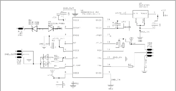
4.3
The gate driver schematic and prototyping
The important considerations are kept in mind while designing the layout for high frequency gate drivers for example parasitics can heavily influ-ence the gate signals for SiC devices and can be deleterious for overall system [34]. The complete schematics design for gate driver (a) Ucc27531 chip from the topology shown below in the Figure 26. Extra decoupling
MGJ2D121505SC DC-DC converter for driver modules power supply
Nominal Input Voltage 12V
Output Voltage 1 15V
Output Voltage 2 -5V
Output Current 1 80mA
Output Current 2 40mA
Input Current at Rated Load 120mA
Ripple & Noise (Typ)2 30 mVp-p
Efficiency (Typ) 80%
capacitors are added to the power supply for a steady output needed for gate driver IC for minimizing noise and consuming all energy present.
Figure 26 Gate driver Ucc27531 gate drive tropology
In addition, two gate resistors for Rg-on and Rg-off are added which help to maintain the switching speed of the DUT. Two hyper fast diodes with minimum recovery are added in the design to utilize the different turn-off resistance option in a single output driver like gate driver (b) 1ED020I12-F2. The gate driver boards also include a high accuracy and high PSRR voltage regulator for supplying the required power to opto-coupler and microcontroller for generating PWM signal needed for DPT test board. The IC is supplied by 5.2 KVDC isolated gate driver DC-DC converter, which provides the suitable supplies and isolation required for protection. The isolated DC-DC converter and voltage regulator sche-matic are shown in the Figure 27.
Figure 27 Schematics of (a) DC-DC converter (b) PSSR Voltage regulator
The PCB layout of gate driver is created keeping in mind the shorten traces for minimizing the parasitic inductances as much as possible. All
Figure 28 Schematic view design of gate driver (a) Ucc27531
Few jumpers are applied to the gate driver board to shorten the trace whereas its width is adjusted at a reasonable value for minimizing the parasitic inductances. The 30µF SMD capacitors are added in the design due to achieve higher transient drive.
Figure 30 Schematic view design of gate driver (c) ADuM4135
The gate driver board is a two-layer board, and it is designed in a way on both sides for reducing noise in both layers [35]. In addition to low para-sitic inductance in the gate driver loop, proper creepage and clearance distances are set in the PCB design for preventing insulation failures [36].
Figure 31 PCB layouts for the gate driver modules (a) Ucc27531 (b) 1ED020I12-F2 (c) ADuM4135
A high voltage diode is accounted for the desaturation protection. The gate driver (b) and (c) utilize this diode to block high voltage and measure the voltage drop across diode for DESAT protection features. Figure 31 describes the layout of the board while Figure 32 shows its real appear-ance.
Figure 32 Real appearance of gate driver modules (a) Ucc27531 (b) 1ED020I12-F2 (c) ADuM4135
4.4
Double-Pulse Test Setup Description
The dynamic characterization platform as Double pulse tester is com-monly used to evaluate the switching transients of SiC power discreates. A setup is designed which provides clean and accurate measurements under well-defined conditions which can efficiently correlate to the sim-ulation results of the device. Important driver design parameters like maximum allowed leakage inductance and parasitic capacitance param-eters can be derived from this setup [35]. The dynamic behaviour of the SiC MOSFET is characterized by voltage and current across the DUT dur-ing turn-on and turn-off switchdur-ing under the defined circuit conditions. Consequently, characteristics like dv/dt, di/dt, and gate driver properties can be achieved from our DPT tester.
The tester is designed for DC-Link voltage up to 2KV and a current up to 50A. The PWM pulses for control part are sent by a designed microcon-troller. The DPT can validate 1200V/40A SiC MOSFETs for experimental validation. The real appearance of DPT design setup is show below.
Figure 34 Developed Double Pulse test setup 4.4.1 Load Inductor
The specific load can be set by as an inductor and the pulse widths in the setup. The value of load inductor is calculated as follows:
L ≥𝑉𝑑𝑐∆𝐼
𝐿 =
𝑉𝑑𝑐
𝐾∆𝑖×𝐼𝐿𝑡𝑠𝑤 (1.16)
Where tsw is the time taken by a complete switching event while Vdc and
IL are DC bus voltage and load current, respectively. K.∆i shows the
cur-rent variation percentage during the switching transition ranging 1%–5%. Low limit of the required inductance is calculated in equation 1.18. If the inductance value is high the longer duration must be used for achieving the same current, which in turn causes thermal concern in MOSFET. The inductor used in the testing is a big 480µH inductor.
4.4.2 DC Capacitor bank
Energy is supplied by the two banks with possibility of series and parallel connection with large capacitance which establish the inductive current during the turn-on pulses. The minimum value for Cbulk is:
Figure 35 DC-link board capacitor schematic
By changing the different jumpers, two capacitance levels of 100µF for 1.2 KV and 50µF for 2 KV can be achieved.
4.4.3 Bleeder resistor
For safety reasons, two resistors are in parallel with the capacitor bank to discharge the capacitors under the condition when the test setup is turned off but also to balance the voltage across the capacitors. Rbleeder is based on
trade-off between the power loss and the discharge time.
𝑃 𝑏𝑙𝑒𝑒𝑑𝑒𝑟 = 𝑉𝑑𝑐2 𝑅 = 8002 300×103= 4.8 𝑊
(1.18) 𝑇 𝑑𝑖𝑠𝑐ℎ𝑎𝑟𝑔𝑒= 𝑅𝑏𝑙𝑒𝑒𝑑𝑒𝑟× 𝐶𝑏𝑢𝑙𝑘= 300 × 10 3 × 50 × 10−6= 15𝑠 (1.19)
In the final design, bleeder resistor consists of two 300 kΩ, 5W metal oxide film resistors in the series [35]. For voltage balance of the capacitor bank,
these two resistors are also in parallel with series-connected energy stor-age capacitors individually as seen in the Figure 35.
4.4.4 The device board
The device board is designed for different TO packages and device board is mounted on DC-link board so that inevitable common source induct-ance can be minimized. For minimizing effective length of power devices, a gate driver board is placed on the device board directly in the way that two boards are connected with each other through the same connecter. Here, in the PCB the positive and negative planes are overlapping, with an isolation layer between them. Hence, the two planes overlapping thus giving a minimal parasitic inductance.
Figure 36 Device board placement
The parasitic minimization placement is based on minimization in the gate loop and power loop and components are placed as close as possible to each other [14]. RF connectors are placed just next to the device for voltage and currents measurements and a direct connection is made us-ing a small coil thus resultus-ing in minimization of group loop for oscillo-scope. As a result, the lead lengths in both power and gate loop are re-duced significantly. Parasitic minimization placement comparison is given in table below.
zation placement
4.5
Measurement of voltage and currents
4.5.1 Oscilloscope selectionIn a DPT, oscilloscope is being considered as the first measurement tool capturing the waveforms of the switching transients. The frequency de-pends on duration of the ramp and is independent to the voltage/current slew rate. For capturing the enough detail of a waveform, the bandwidth of the oscilloscope and the sampling rate should be higher than the equiv-alent frequency. WBG transients occur in the order of few nanoseconds. Thus, faster sampling rates and higher bandwidth improve the detail of the waveform. Tektronix MSO064 Mixed Signal oscilloscope is used for DPT measurements exhibiting features like sampling rate of 25 GS/s, and bandwidth rate of 8GHz to determine the accurately measured fastest switching transients. In addition, the oscilloscope provides the horizontal resolution to a maximum scale.
4.5.2 Voltage probe and current measurement
A 1GHz bandwidth voltage single-ended probe is selected which can measure voltage up to 300Vp-p. The voltage probe is manifested with low input capacitance specification (< 4 pF) for minimizing the loading effect of probe on the DPT circuit. Moreover, to obtain noise free measurements the ground path is shorted. Considering current measurement in DPT, inserting switching current measurement into switching loop is neces-sary, which affects the power-loop layout. In order to introduce the layout design and current measurement taken into account for the DPT, shunt resistance 50mΩ is added on low side for measuring the current in DPT setup [20]. The insertion inductance introduced by the shunt resistor is measured and was considered negligible.
5
Results and discussion
5.1
DPT test results
During the operation, two pulses are fed to the gate of SiC device for switching the device. The current though the inductor ramps up to re-quired level during the first pulse before the DUT is turned-off. The turn-off transients are measured on the falling edge of first pulse (t1).
Mean-while the turn-on trainsets are captured at rising edge of the second pulse (t2). The switching voltage can be adjusted with the voltage VDC and the
current with the inductor charge time t1. The implemented test conditions
are illustrated in the Table 8 below. The typical logic signals observed in the double pulse signal is shown in the Figure 37, where -5V and +15V being low and high respectively relative to circuit ground.
Table 8 Parameters of double pulse test setup
Figure 37 Timing scheme for double pulse test
Test conditions
Value
SiC Diode C3D25170H VDC 300 V Id 15A L 480 µH CDC 100 µF (to – t1) 24 µs (t1 – t2) 0.8 µs (t2 – t3) 1 µs
resistance and gate drivers are not identical, a rough analysis performance for the devices is achieved from the data sheets supplied by manufacturers.
Table 9 Basic switching comparison of SiC MOSFETs
Device Ciss (pF) Coss (pF) Turn-off En-ergies Turn-on En-ergies ROHM-SCT2080KE 2080 77 55 µJ 174 µJ Cree-CMF20120 1915 120 155 µJ 125 µJ Little-fuse 120E0080 1700 82 50 µJ 130 µJ
Alignment of the VDS drain-source voltage and IDS drain- source current
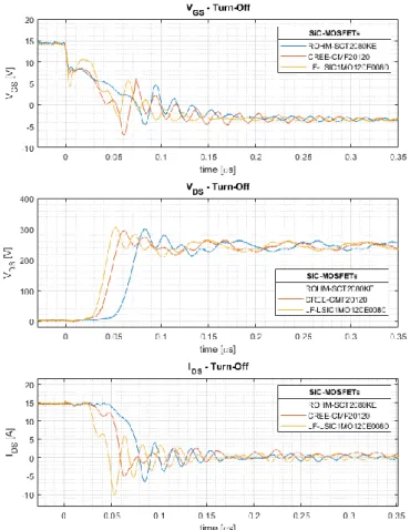
and setup implementation are done in the same manner [34]. Because of the high-speed voltage transients of SiC, the switching transients result into high dV/dt as 100V/μs imposes common mode problems in the driver circuit. In addition, extreme dV/dt stress reduces the lifespan of the insulation material over time [37]. Different factors for the SiC power de-vices like rise time, fall time, and delays between turn-on and turn-off are usually different, and thus require individual consideration. The relation-ships between VGS, VDS, ID and Rg are investigated in all the devices as
Figure 38 Comparison of different SiC Switches during Turn-on
The internal gate resistance of the SiC MOSFET ROHM-SCT2080KE, Cree-CMF20120, and LittleFuse-LFE0080 is 4Ω, 5Ω and 0.6Ω respectively, Due to lower internal resistance Rg-int the Little-fuse and Cree MOSFETs show the fastest rise and fall times but generate higher interference in EMI due to fast dI/dt. The output capacitances of the MOSFET also plays important role in EMI generation during transients. In SCT2080KE MOSFET VDS shows better performance in turn-on transition. The SiC
MOSFET from CREE-CMF20120 performs better in turn-off transition but generates higher ringing on the gate voltage.
Figure 39 Comparison of different SiC switches Turn-Off
The SiC SCT2080KE switch has minimum threshold voltage 1.6V. The typical temperature coefficient of the threshold voltage is -5mV/C0 [11].
Operation at an elevated junction temperature of 175 °C results in a threshold shift to roughly 1.6 V – (175–25) * 5 mV = 0.85 V. The output capacitance of the selected device is the minimum among other device i.e around 77pF. The ROHM SCT2080KE MOSFET improves the efficiency of overall system by delivering a steep rise and fall time that increases the application performance but limiting the excessive EMI.
5.3
Silicon carbide Schottky Diodes(SBDs)
The reverse recovery effect seen in the SiC switches heavily influence the switching losses in turn on period. The reverse recovery losses can be eliminated if the silicon freewheeling diodes are replaced with the latest schottky barrier diodes (SBDs) [38]. The SBDs exhibits very low reverse recovery charge Qrr due to its very low junction capacitance. SBDs are independent of forward current, temperature, and high dI/dt. The