Technical report, IDE1059, November 2010
Electrical and Optical Characteristics of InP Nanowire
based p-i-n Photodetectors
Master’s Thesis in Electrical Engineering
Rizwan Ahmed, Shahid Abbas
School of Information Science, Computer and Electrical Engineering Halmstad University
Electrical and Optical Characteristics of InP Nanowire
based p-i-n Photodetectors
Master’s thesis in Electrical Engineering
School of Information Science, Computer and Electrical Engineering
Halmstad University
Acknowledgments
All Praise and Thanks to ALLAH ALMIGHTY, the most BENEFICIENT & the most MERCIFUL, WHO made all this possible for us.
First of all we would like to thank our supervisor Håkan Pettersson for giving us the opportunity to work in this interesting and cutting edge field and for his precious time and help. It was a real pleasure to work with him and to learn from such an expert scientist.
We would also like to thank Lars Landin who also helped and shared knowledge with us when it was necessary.
Profound thanks to the program coordinator, Jörgen Carlsson for always keeping the doors open, ready for discussions during studies. He is the person who made us able to see and think about things with close eye.
Special thanks go to the Lund Nano Lab for fabricating the nanowire photodetectors for our experiments.
A special thanks to all our beautiful friends and cute lovers at this moment, who make our life outside work enjoyable!
Especially grateful to our caring brothers, sisters & all family members for always being there for encouragement & solid support.
Love to all cutest & sweetest children in our families.
We, of course have no words for parents to say them thanks for their love, care and prays for us. But the overall dedication for the thesis goes to the respectable parents.
I have feelings of thankfulness and appreciation which cannot be expressed in words for elder brothers, Mumtaz Hussain and Imran Qaisar, for their enormous encouragements and financial support. Without the support of these people, it would have been impossible to reach here.
(Rizwan Ahmed).
My sincere gratitude to M.Ikram.N, M.Ahsan, Hamid.G & enormous gratitude to my elder sister and brother in law, M.Asif for their motivations, all the time.
(Shahid Abbas).
We are glad and feel a pleasure after completing our task while working together, our collaboration make this research based thesis project an enjoyable work for us. We wish to do research together in the future.
Rizwan Ahmed, Shahid Abbas
Abstract
Photodetectors are a kind of semiconductor devices that convert incoming light to an electrical signal. Photodetectors are classified according to their design, operational principle and spectral sensitivity. Infrared photodetectors are widely used in many applications such as night vision, thermal cameras, remote temperature sensing, and medical diagnosis etc.
All detectors are fabricated from materials that are sensitive to incoming light. One important type of photodetectors, so called photon detectors, absorb photons and form a photocurrent as the excited charge carriers are swept away by an electric field.
In this project Fourier Transform Infrared (FT-IR) Spectroscopy is used to investigate a new kind of photodiodes that is based on self-assembled semiconductor nanowires (NWs) which are grown directly on the substrate without any epi-layer. The spectrally resolved photocurrent (at different applied biases) and IV curves (in darkness and illumination) for different temperatures have been studied, respectively. Polarization effects (at low and high temperatures) have been investigated. The experiments are conducted for different samples with high density of NWs as well as with lower density of NWs in the temperature range from 78 K (-195ºC) to 300 (27ºC). These photodiodes are designed to work in near infrared (NIR) spectral range.
The results show that the NW photodetectors indeed are promising devices with fairly high sensitivity and a fairly high break down voltage. There are also interesting polarization effects that need further investigations. The impact of different polarized light on photocurrent spectra has been investigated and an attempt has been made to clarify the observed double peak of InP photocurrent spectrum. Our investigations also include a comparison to a conventional planar InP p-i-n photodetector.
Abbreviations:
L Light I Current V Voltage IR Infrared UV Ultraviolet D Darkness T Temperature W Wavenumber NWs NanowiresNIR Near Infrared MIR Mid Infrared LIR Long Infrared Ea Activation Energy TMI Trimethylindium TMG Trimethylgallium ITO Indium Tin Oxide TBA Tertiarybutylarsine meV Mili Electron Volt VLS Vapor Liquid Solid Epi-layer Epitaxial Layer
TBP Tertiarybutylphosphine CVD Chemical Vapor Deposition FT-IR Fourier Transform Infrared ITO Intelligent Temperature Controller MOVPE Metal Organic Vapor Phase Epitaxy FOV Field of View
Table of Contents
CHAPTER 1: INTRODUCTION ... 1
1.1 GOAL ... 1
1.2 MOTIVATION ... 1
1.3 BACKGROUND ... 2
1.3.1 External photoeffect / Photoelectric effect ... 3
1.3.2 Internal photoeffect ... 3
1.3.2.1 The p-‐n photodiode ... 4
1.3.2.2 The p-‐i-‐n photodiode ... 6
CHAPTER 2: SAMPLE DESCRIPTION ... 9
2.1 NANOWIRES (NWS) ... 9
2.1.1 Growth of nanowires ... 9
2.2 METAL ORGANIC VAPOR PHASE EPITAXY (MOVPE) ... 9
2.3 DESIGN OF THE SAMPLE ... 11
2.3.1 Isolation ... 13
CHAPTER 3: EXPERIMENTAL SETUP ... 16
3.1 FOURIER TRANSFORM INFRARED SPECTROSCOPY (FT-‐IR) ... 16
3.1.1 FT-‐IR Parts ... 16
3.1.1.1 The FT-IR Spectrometer ... 16
3.2 KEITHLEY 2602A SOURCEMETER® INSTRUMENT ... 23
3.3 KEITHLEY 428 CURRENT AMPLIFIER ... 23
3.4 POLARIZER ... 24
3.5 SYSTEM PREPARATION FOR THE EXPERIMENTS ... 25
CHAPTER 4: MEASUREMENTS AND RESULTS ... 26
4.1 OPTICAL PROPERTIES ... 26
4.1.1 High density sample ... 26
4.1.2 Low density sample ... 30
4.1.3 Mesa structure p-‐i-‐n photodiode ... 31
4.1.4 Combined plots ... 34
4.1.5 Reference Si photodiode ... 36
4.2 ELECTRICAL PROPERTIES ... 37
4.2.1 High density sample ... 38
4.2.2 Low density sample ... 40
4.2.3 Mesa structure p-‐i-‐n photodiode ... 45
CONCLUSION ... 48
INTRODUCTION
Chapter 1
: INTRODUCTION
The study of semiconductor materials reveals that during the recent years, dramatic improvement has been seen in electronic and photonic devices. The size of the devices has been reduced, their power consumption has been minimized and their performance has been improved. The photodetector belongs to one of the most interesting photonic devices.
Photodetectors is a kind of semiconductor device that detect and convert incoming light to an electrical signal. Photodetectors are classified based on their different design, operational principle, applications and different spectral sensitivity. Specific photodetectors have been developed depending on the level of desired wavelengths to be detected e.g.; from the region of ultraviolet to the infrared region. The samples we are investigating are designed to detect near-infrared (NIR) wavelengths.
1.1 Goal
The goal of the project is to analyse a new kind of photodiodes that are based on self-assembled InP NWs directly grown on the substrate without any epi-layer. Fourier Transform Infrared Spectroscopy (FT-IR) is used to analyse the optical properties. The photocurrent is measured and analysed for different temperatures (78K to 300K) and different applied biases. IV curves in darkness and illumination at different Temperatures (78K to 300K) are analysed. Polarization effects on photocurrent spectrums are analysed at low and high temperatures with NIR as light source.
All the experiments were conducted for different samples with high density as well as with low density of NWs at different temperatures (78K to 300K). These photodiodes are designed to work at NIR wavelengths. All results for different samples are compared to each other and to the results of a conventional planar InP p-i-n photodetector.
1.2 Motivation
Silicon is by far the most important semiconductor material for the electronics industry e.g. due to its great abundance on the earth, the possibility to form excellent thin SiO2 insulators and the
relatively large bandgap (compared to e.g. germanium). Unfortunately, silicon has indirect band gap which draws some limitations to use it in the optoelectronics devices which are based on direct band gap material. Figure 1 shows the band gap structure of direct and indirect band gap material.
Optoelectronic devices are often made of group III-V binary compounds (InAs, GaAs, InP etc). The performance of these devices has improved so fast during recent years. As described earlier there are different types of photodetectors for specific purposes, some of these are based on the interest of wavelength detection level (UV to IR). Detection at IR wavelengths is important for night vision, astronomy, communication, medical diagnosis etc. IR is invisible to human eye. The
INTRODUCTION
range of IR wavelengths is from 700nm to 1mm with further division into three classes as show in Table 1. Valence Bnad Conduction Band Si Valence Bnad Conduction Band InP, GaAs (a) (b)
Figure 1: Energy band structure (a) indirect band gap (b) direct band gap
Table 1: Infrared light range
NIR (Near Infrared)
700nm to 1400 nm
MIR (Mid Infrared)
1.4µm to 3µm
LWIR (Long Wave Infrared)
3 µm to 1000µm
The investigated samples in this thesis are used to detect NIR wavelengths. The NIR wavelength region is commonly used in fibre optic communication system for its low loss. So we have used NIR source for the analysis under different conditions. We were concerned with NIR but sometimes it is useful to take some readings with MIR source in order to see defects and sensitivity for longer wavelengths. The reasons and motivations for choosing the more complicated structure which is based on NWs instead of simple structure are discussed in chapter 2, where sample (photodetector) descriptions are presented along with its characteristics.
1.3 Background
Photodetectors are semiconductor devices that detect incoming light and convert it into an electrical signal. Basic operation of photodetectors can be demonstrated in 3 steps.
(i) Carrier generation
INTRODUCTION
forms an electric current. There are two systems to detect the incoming photons and generate the carriers: external and internal [1].
The above process is called a photo effect and it is further classified in two types: (i) External photoeffect
(ii) Internal photoeffect ( most of the modern photodetectors are based on the internal photoeffect)
1.3.1 External photoeffect / Photoelectric effect
A collision between an incoming photon and a material’s surface in vacuum that leads to the escape of an electron from the material over a potential barrier into the vacuum as a free electron is called photoelectric emission. This process will happen if the incoming photon has larger energy than the work function,W, [1]. This is demonstrated in Figure 2.
W Ema Conduction Band Free Electron Photon Fermi level Vacuum level
Figure 2: Energy levels of metal
Figure 2 shows the energy levels of a metal for the external photoeffect (photoelectric effect). Photodetectors which are based on the external photoeffect require vacuum surrounding them. That’s why these are usually used in vacuum tubes. Some metals can be added as amplifier inside the tube in order to have a good signal. Higher amplification than 107 can be achieved.
1.3.2 Internal photoeffect
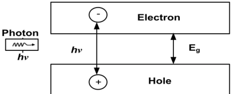
In this phenomenon, there is no need of vacuum for the excited electrons. Instead the generated charge carriers (electrons & holes) stay inside the semiconductor. There is a photoconductive material inside these photodetectors which generates electron-hole pairs as a result of absorbed light. Incoming photons excite electrons from the valence band to the conduction band. By applying an electric field the generated photocarriers (electron-hole pairs) will be transported through it, producing the photocurrent in the external circuit of the detector as shown in Figure 3 [1].
INTRODUCTION Electron Hole Eg hv -+ Photon hv
Figure 3: Electron-hole photo generation in a semiconductor
The famous models for photodetectors that are based on the internal photoeffect are p-n photodiodes, p-i-n photodiodes, heterostructure photodiodes, Schottky-barrier photodiodes and array detectors. Each of these detectors has special manufacturing technology, properties, advantages and disadvantages. According to the application these can be selected for specific purposes [2, 3].
Since, the entire investigated samples 6549A & 6549B (high concentration of NWs) and 6550A (low concentration of NWs) in this project are of p-i-n type, we briefly discuss p-n and p-i-n photodetectors models.
1.3.2.1 The p-n photodiode
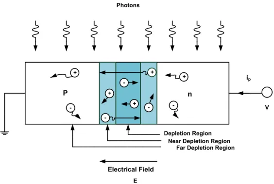
The p-n photodiode is a semiconductor that has two blocks, one is p-doped and the other one is n-doped. When these two oppositely doped blocks are brought in contact, a junction is formed with a depletion region that contains a very high built-in electric field. Light is absorbed in this region and carriers are generated. These carriers are separated by the electric field. Basically, the illuminated p-n junction can be divided in three regions as shown in Fig. 4.
(1) Depletion region (middle) (2) Near to depletion region (3) Far from depletion region A p-n photodiode under illumination and reverse bias is shown in Figure 4.
INTRODUCTION P n -+ -+ -+ -+ + Depletion Region Near Depletion Region
Far Depletion Region
Electrical Field Photons
E
V ip
Figure 4: p-n photodiode under illumination
Figure 5 shows the effect of illumination on the IV curve. Without illumination the current is zero at 0V applied bias. With illumination, the IV is shifted downward due to the large negative photocurrent. If we increase the light intensity, the IV curve shifts downward proportional to the intensity.
Id
Vd
Dark Current
Increasing Light Intensity
IL
Figure 5: Effect of increasing light intensity and dark current
Figure 6 shows the energy band diagram of the p-n photodiode. When photons with energy larger than the band gap energy, are absorbed, electron hole pairs are generated. Holes will move to the p-side where we have applied negative potential and electrons will move to opposite side as shown by the diagram. So reverse currents flows in the circuit.
INTRODUCTION Electron Hole EC EV Eg
Figure 6: Energy band diagram of p-n photodiode
(1) Depletion region: In the middle, the depletion region is formed. Here electrons and holes are generated. Both drift quickly in the opposite directions (electrons move to n-region, while holes move to p-region) due to the applied negative voltage.
(2) Near depletion region: Near the middle region, both the electrons and the holes have the chance to contribute to the current by entering the depletion region due to diffusion.
(3) Far from depletion region: In this region, the electrons and holes will recombine randomly and they do not contribute to the photocurrent.
The depletion region must be kept small to reduce the transit time. On the other hand, to increase the quantum efficiency, the depletion layer must be sufficiently thick to allow a large fraction of the incident light to be absorbed. Thus, there is a trade-off between the response speed and quantum efficiency [2].
In conclusion, most of the photocurrent is generated in the depletion region. So, with wider depletion region, we can have higher photocurrent by trapping more photons in the depletion region. In order to have a wider depletion region, we can add an intrinsic layer between the n and p-doped regions [1, 3].
1.3.2.2 The p-i-n photodiode
The p-i-n photodiode is a photodetector with an intrinsic layer in the middle of the p-n junction. The p-i-n photodiode is one of the most common photodetectors because the depletion region (the intrinsic layer) can be tailored to optimize the quantum efficiency and frequency response. A simplified diagram of the p-i-n photodiode is shown in Fig. 7 [2].
INTRODUCTION i n P L D W
Figure 7: p-i-n photodiode structure
The intrinsic layer is an extension of the depletion region. This extension of the depletion region has some advantages compared to the ordinary p-n junction.
(1) Increasing the width of the depletion layer increases the volume for absorbing more light.
(2) Increase in the width of the depletion layer reduces the capacitance of junction which reduces the RC delay but the transit time increases.
(3) By reducing the ratio between the diffusion length and the drift length of the device a generated current is in greater proportion being carried by the faster drift process.
Photodiodes are usually used in the strong reverse bias because with stronger reverse bias, the depletion region increases (more important for p-n junctions); therefore more light can be absorbed. Besides this, the electric field in the junction increases which increases the drift velocity of carriers in the depletion region.
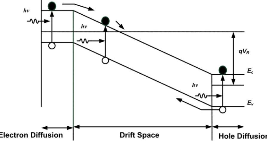
Figure 8 shows the cross section of the p-i-n photodiode that has an antireflection coating to increase the quantum efficiency. Figure 9 shows the energy band diagram of the p-i-n photodiode under reverse bias condition. As can be seen that depletion region has been increased due to the intrinsic layer. So when light will be absorbed in the semiconductor, electron-hole pairs will be generated. Pairs produced inside the depletion region (or within a diffusion length from the depletion region) will be separated by the electric field as shown in Figure 9. So, a reverse current flows in the external circuit as carriers drift across the depletion layer [2].
i Antireflection coating Metal Contact n+ p+ + SiO2 hv
INTRODUCTION Ec Ev qVR hv hv hv
Drift Space Hole Diffusion Electron Diffusion
SAMPLE DESCRIPTION
Chapter 2:
SAMPLE DESCRIPTION
2.1 Nanowires (NWs)
Nanowires (NWs) with diameters of the order of 10 nm are sometimes referred to as one-dimensional (1-D) materials because charges are allowed to move in only one dimension. The confinement of charges in the other two dimensions gives new properties of NWs which are different from those in 3-D or bulk materials [4]. There are many applications of NWs in certain fields e.g. electronics, photonics, thermoelectricity, chemistry and bio-medicine. The investigated photodetectors in this thesis are realized in InP which is a very important semiconductor material. The sample’s design and characteristics will be discussed in the subsequent sections.
2.1.1 Growth of nanowires
There are different methods for the fabrication of NWs and all can be divided into two groups. (i) Top-down
(ii) Bottom-up
Top-Down: Lithography is the main strategy for the top-down method. To achieve better quality, as well as higher density of NWs on the substrate, we need to use the bottom-up strategy.
Bottom-Up: vapour-phase growth and solution-based growth are the two common techniques to get high density along with high quality [5, 2].
Vapour Phase Growth (VPG): This approach is widely used today. In this method the material is in vapour phase. Usually, there is some catalyst at the top of the substrate where the material of the substrate and NWs can be either the same or different. The investigated samples during this thesis work are fabricated using MOVPE (metal organic vapor phase epitaxy).
Solution based growth: This method is basically more common for the inorganic materials. In this approach, some templates of porous alumina are used. During this method, due to the electrodeposition, the NWs are guided inside the templates. The templates are removed when the process of electro deposition is completed for growth of NWs.
2.2 Metal Organic Vapor Phase Epitaxy (MOVPE)
In this technique, the metal organic precursor vapours are the sources for the fundamental atoms of the growing layer. For example, to fabricate a GaInAsP (III-V materials) semiconductor, trimethylgallium (TMG), tertiarybutylarsine (TBA), trimethylindium (TMI) and
SAMPLE DESCRIPTION
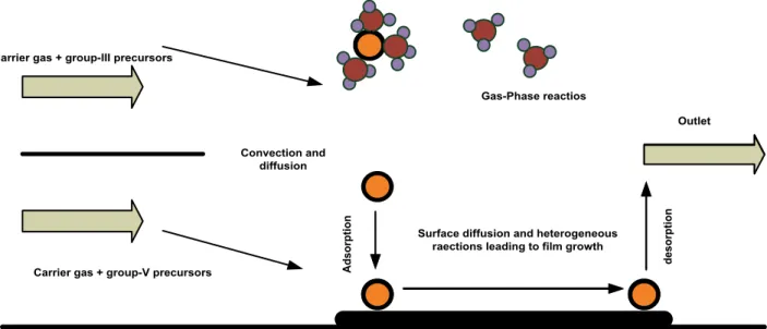
tertiarybutylphosphine (TBP) are used. Schematics of a MOVPE system and the whole growth process are shown in Figure 10 [7].
The system consists of a quartz glass reactor and some gas lines. Hydrogen is injected through bubblers containing the metal organic precursors. Nitrogen or Hydrogen carrier gas is used to bring the precursor vapours to the reactor. A computer (having mass flow controller) is used to control the flow of vapours. The temperature of precursor container is stabilized with a bath that also helps to control the pressure of the bubblers.
TMI TBP TBA
Bubblers in Temperature Stabalized baths
H2 N2 Exhuast TMG Halogen Heater Thermocouple Quartz Reactor Substrate
SAMPLE DESCRIPTION
Wafer
Carrier gas + group-V precursors Carrier gas + group-III precursors
Convection and diffusion Gas-Phase reactios Outlet A d so rp ti o n d es o rp ti o n
Surface diffusion and heterogeneous raections leading to film growth
Figure 11: MOVPE process
The substrate (wafer) is inside the reactor, at the top of a graphite plate that can be heated up by a halogen or RF heater. A thermocouple is used to control the temperature of the graphite and substrate. Some major processes in MOVPE are the following:
• Mass transport from the vapour phase to the substrate surface. • Precursor molecule decomposition and atom adsorption. • Atom diffusion on the substrate surface.
Nanowires are formed by self-organization, atom by atom, in a highly controllable manner. Usually, there is some catalyst particle at the surface of the substrate. Among other different elements, gold is the most commonly used catalyst particle to get different types of nanowires at a wide range of growth conditions. The diameter of the gold nanoparticles determines the diameter of the NWs. Gold forms a eutectic alloy with the substrate material at the growth temperature. When the precursor materials come into contact with the alloy, a super saturation of the alloy initiates the preferential growth under the gold particles. By controlling the growth parameters more complex nanostructure can be formed. Figure 11 shows the process of MOVPE.
2.3 Design of the Sample
The investigated photodetectors in this thesis project are based on an ensemble of InP NWs grown on an InP substrate, some general information and important characteristics of the samples are described here for the better understanding of the sample. But due to some marketing trends and policies, the detailed production technology is not allowed to be discussed here.
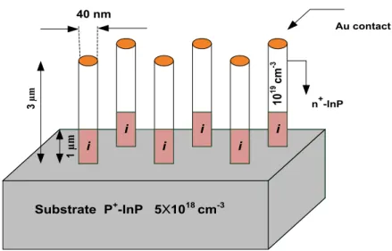
NWs are directly grown on the substrate from 40 nm gold seed particles as previously described. The InP substrate is p-type and the NWs are n-type with an initial nominally undoped (intrinsic) region. The general design of the sample is shown in Figure 12.
SAMPLE DESCRIPTION i i i i i Substrate P+-InP 5X1018 cm-3 n+-InP 10 19 cm -3 40 nm 3 µm 1 µ m i i i i i i i Au contact
Figure 12: Schematic of the InP nanowire photodetector
When the NWs are grown, firstly an intrinsic layer with the length around 1µm is formed. The advantages of this intrinsic material have been discussed earlier. After the intrinsic layer the growth of the NWs starts with high n-type doping. In our study, we have investigated samples with different surface density of NWs (0.2µμm-2 and 10µm-2). All the samples on the piece of
wafer are connected to the same back contact A. Experimental results in the thesis are achieved for samples with difference piece of wafer. We have chosen the samples which gave a strong signal under illumination. The description about the samples is shown in the Table 2 below. The samples marked in bold style had the best signal. Other samples do not show a strong photosignal.
Table 2: Specification of the samples
Samples Name
Characteristics
Sample 6549A Sample 6549B Sample 6550A
Impurity (Zn) concentration
in the InP substrate 5
X1018 cm-3 5X1018 cm-3 5X1018 cm-3
Length of Intrinsic layer 1µm 1µm 1µm
Length of NWs 3µm 3µm 3µm
Diameter of a NWs 40nm 40nm 40nm
Impurity concentration in
theInP NWs 10
19 1019 1019
Surface density of InP NWs
on InP substrate 10 NWs/ µm
SAMPLE DESCRIPTION
2.3.1 Isolation
To connect all the NWs in parallel without a short circuit, it is necessary to isolate them with SiO2 (a good isolator) as shown in the Figure 13. Next step is to remove this SiO2 from the top of
the NWs by a back-etching procedure. ITO (indium tin oxide) is used as a transparent film to connect all the NWs in parallel as shown in Figure 14. ITO, being both transparent to wavelengths in the NIR region and highly conductive has a lot of applications in optical devices and is very useful for the NW-based photodetectors.
SiO2 Substrate +p i i + n + n
Figure 13: Isolation of the NWs
+ -i i i i i SiO2 ITO Substrate
SAMPLE DESCRIPTION
qVR
hv
P+ Intrinsic n+
Figure 15: Energy band diagram along a NW under reverse bias
Figure 15 shows the energy band diagram of our samples along a NW. Since our samples are based on p-i-n junctions, the energy band diagram is similar to the energy band diagram of conventional p-i-n photodetectors. In our case, most of the light will probably be absorbed by the substrate and generate electron-hole pairs that diffuse to the depletion region at the NW/substrate interface. A fraction of the light will be absorbed directly in the depletion region of the NWs, where the electric field will separate the electron hole pairs and cause the current to flow in the external circuit.
There are a number of reasons for using the more complicated structure based on NWs instead of using e.g. a conventional simple mesa structure. A few reasons are described below
• If a certain region of the mesa structure photodiode becomes short-circuited, then the whole photodiode is useless. But in the case of NW-based photodetectors, if one NW becomes short-circuited then it will act as a fuse and break. The other NWs will probably still be OK so the complete device will not be destroyed. It is illustrated in the Figure 16.
SAMPLE DESCRIPTION + -i i i i i SiO2 ITO Substrate i
Figure 16:Schematic of NWs based p-i-n photodiode
• The most important advantage is that optically active NWs can be grown directly on a cheap silicon substrate. Besides a lower cost, it will be possible to integrate the necessary readout electronics directly on the same silicon chip as shown in the Figure 17.
Silicon Substrate
Figure 17: Schematic of the NWs grown on Silicon substrate
• The small size of the NWs is expected to provide e.g. higher sensitivity and reduced noise compared to planar detectors.
EXPERIMENTAL SETUP
Chapter 3:
EXPERIMENTAL SETUP
In this section, the experimental setup and the specifications of the instrument are discussed which is used during our experiments. The whole experimental setup includes a Bruker Vertex 80V Fourier transform infrared spectrometer (FT-IR), a Keithley 428 current amplifier, and a Keithley 2602A SourceMeter, Nitrogen (liquid), Nitrogen (gas) and Helium (gas) are used for different purposes during experiments.
3.1 Fourier Transform Infrared Spectroscopy (FT-IR)
In this thesis project, FT-IR is used to test the optical properties of the photodetectors. These properties are investigated to check the quality and response of the sample. Actually, infrared spectroscopy is an experimental technique used to:
• check the quality of the sample and to see if there are any defects • find out the kind of materials used in a sample
• determine the spectral sensitivity of a sample
In this section various parts of the FT-IR along with working principle are discussed. Preparation of the instruments for the experiment will be discussed later.
3.1.1 FT-IR Parts
In the following sections, we discussed the different system components of our set-up more in detail.
3.1.1.1 The FT-IR Spectrometer
This section is about the spectrometer and different components inside the spectrometer. The mechanisms used for the experiments are also discussed briefly. The spectrometer is an evacuable and fully digital system. The specifications of the spectrometer are described in the following Table 3 [10].
Table 3: Specifications of the spectrometer
Specifications of the spectrometer
Spectroscopy model Vertex 80V
EXPERIMENTAL SETUP
AAR (automatic accessory recognition): It recognizes the accessories that are installed in the sample compartment automatically. It also performs several tests and loads the corresponding experiment file automatically, including the predefined measurement parameters.
ACR (automatic component recognition): ACR identifies automatically the installed optical components, such as beam splitter and source detector. This data will be sent to the OPUS (application software). The main purpose of ACR is to enable the user to select the right optics parameters in the application software (OPUS). This is of great advantage.
Performance guard: Besides this, all the components of the spectrometer can be permanently monitored to be sure that they are working in the range of specification so called the function of the ‘‘Performance Guard’’. The main purpose of it is fault recognition and maintenance [10]. The vacuum spectrometer houses built-in light sources, a Michelson interferometer and several different detectors. The description about the detectors will be discussed later. The possibility to evacuate the spectrometer prevents the effects of absorption in water vapour (H2O) or Carbon
Dioxide (CO2), which would give erroneous results in measuring the photocurrent. A vacuum
pump is used to provide the vacuum condition that is oil-free, which prevents introducing the oil vapour inside the spectrometer accidentally. Spectrometer’s components are discussed below.
3.1.1.1.1 Cryostat
The cryostat is one of the main parts of the FT-IR system. The FT-IR installed at Halmstad University has a cryostat with specifications discussed below.
Table 4: Cryostat Brand Information
Cryostat name Made by
Optistat DN Oxford instrument
Optistat DN: It is a top loading and static exchange gas cryostat with optical access provided via four sets of radial and one set of axial windows. The specification table for Optistat DN is given
below in Table 5 [9].
Table 5: Specification of Optistat DN cryostat
Cryostat weight (Kg) 5
Optical port 5 (4radial, 1 axial)
Sample space(mm) Sample space(mm)
Temperature range (K) 77K-300K
Temperature stability (K) ±0.1
Cool down from ambient (min) ~20
Liquid nitrogen capacity (L) ~1.2
Hold time at 77K (hours) ≥15
EXPERIMENTAL SETUP
A schematic diagram of this cryostat is shown in Figure 18.
The cryostat is mounted in the sample compartment of the spectrometer using a tailor-made adapter as seen in the Figure 18. There is a liquid nitrogen reservoir in the upper part of the cryostat. With the help of a capillary tube, it supplies liquid nitrogen to the heat-exchanger. The flow of liquid takes place by gravity and an exhaust valve (placed on the top of the sample tube) helps to control liquid flow. The reservoir and sample space are thermally isolated from the surroundings by the outer vacuum chamber (OVC). This space is pumped to a high vacuum value (10-4 mbar) before the cryostat is cooled down. The cryostat has two sets of windows (inner and outer windows) transparent in the IR spectral range. The inner windows are sealed by indium wires to be air-tight at low temperatures. The temperature can reach 77k with liquid nitrogen. The temperature can be accurately controlled (+/- 0.1K) between 77K and 300K by a temperature controller unit [9]. Helium gas is used inside the sample space to transfer heat from the sample to the surrounding cold walls.
EXPERIMENTAL SETUP
Vacuum Medim Access to Sample place
Sample place execution and pressure relief valve
Liquid Nitrogen Intake
10 Pin Electrical access connector
Exhuast needle valve OVC evacuation and pressure relief Valve
Optistat DN
Liquid Nitrigen resevoir exhuast
Sample Holder
EXPERIMENTAL SETUP
3.1.1.1.2 Light sources
The basic instrument is equipped with a MIR source. The MIR light source is a globar that emits mid-infrared light (i.e. a U-shaped silicon carbide piece). Besides the standard MIR source (air-cooled), following optional sources are available with the specifications listed in the Table 6 [10].
Table 6: Light sources in the spectrometer
We used the NIR source for all our experiments. The spectral range of the IR can be switched from Near Infrared (NIR) to Medium Infrared (MIR) using the computer interface. The source can be switched OFF if someone wants to analyse the electrical signal without illumination. The aperture (which controls the amount of light) is also controlled from the computer.
3.1.1.1.3 Laser
The FT-IR is equipped with a HeNe laser. The laser measures the position of the moving interferometer mirror (also called scanner) and is used to determine the data sampling positions. The laser has the following specification.
Table 7: HeNe laser
3.1.1.1.4 Interferometer
The FT-IR is equipped with an actively aligned ultra scan interferometer based on a linear scanner which ensures a spectral resolution better than 0.07cm-1). The linear scanner is supported by an air bearing which requires the connection to a nitrogen line. The optical pathway of the spectrometer is shown in Figure 19 below.
Source name Lamp Situated Specification
VIS/NIR source Tungsten halogen lamp Installed in the spectrometer
-
UV source Deuterium lamp Connected externally to the
spectrometer
Air-cooled
High power MIR source Globar Installed in the spectrometer
-
EXPERIMENTAL SETUP
modulated in a unique way and the interferometer output is a signal containing all frequencies of IR coming from the source. The interferometer output signal versus position of the moving mirror is called an ‘’interferogram’’. Schematic of interferometer is shown in Figure 19. The interferogram is converted to a spectrum using the Fourier transform as discussed below.
IR Light Source iris M o ve ab le m ir ro r Beam Splitter Sample(detector) Fixed M irror
Figure 19: Schematics of interferometer
Let the change in the distance is ∆d. It is clear from the Figure 19 that interferogram is the
function of ∆d.
Case 1: In case of monochromatic input signal, wave number= δ0, the expression for the output
signal is
I (∆d) = 2I0 (1+cos (4π∆dδ0)) Eq.3
I0 = Intensity of the partial beams.
EXPERIMENTAL SETUP
Case 2: In case of a broad-band source used instead of monochromatic source, then the expression for the interferogram is given by:
I (∆d) = 20ʃ8 (1(δ) +1(δ) cos (4π∆dδ)) dδ Eq.4
Eq.4 is the output signal when the broad-band signal is used. In this expression the second part is known as the cosine Fourier transform of the total spectrum. The sample that is placed in the path of the beam will interact with different components of the spectrum. Now, the modulated signal from the detector can be converted to a spectrum (i.e. detector signal as a function of wave number) using the inverse Fourier transforms. All of these calculations are done by the computer attached to the FT-IR system. The FT-IR offers much better signal-to-noise ratio compared to conventional grating spectrometers. Also, the measuring time is greatly reduced since all wavelengths are analysed simultaneously [1, 9].
Referring to Figure 20 [10], the schematic diagram of the optical bench of Vertex 80V is shown. Locations of the IR light sources, beam splitters, interferometer, sample compartment and built-in detectors are shown clearly.
50
F
ELECTRONICS IN 1 IN 2 O U T 1 O U T 3 OUT 4 OUT 5 O U T 2 D1 D2 Detector Compartment Sample Position BMS INTERFEROMETER IVU APT NIR SOURCES MIREXPERIMENTAL SETUP
3.1.1.1.5 Detectors
The basic configuration of the spectrometer includes a DigiTect™ DLaTGS detector. The detector contains an analogue-to-digital-converter that converts the analogue signal from the detector directly into a digital signal. This digital signal is transmitted to the data processing electronics unit of the spectrometer. The standard detector is a pyroelectric DLaTGS detector which covers a spectral range from 12,000 to 250cm-1, operates at room temperature and has a sensitivity of D*>4x108 cm Hz1/2 W-1. Apart from the standard detector , there are a large number of optional detectors. All detectors are mounted on dovetail slides which allow an easy exchange. In our experiments, the NW-based photodetectors under investigation act as detectors themselves. The integrated DLaTGS detector is only used to record the spectral content of the NIR source [10].
3.2 KEITHLEY 2602A SourceMeter
®Instrument
This instrument is used as a voltage supply during the IV measurements. Specifications for this instrument are listed in Table 8 [11].
Table 8: Specification of KEITHLEY 2602A Source-Meter instrument
Specification of KEITHLEY 2602A Source-Measure instrument Made in U.S.A
Function Source ±DC voltage Source ±DC current Measure ±DC voltage Measure ±DC current
Capabilities 1µV to 40V 1pA to 3A 1µV to 40V 1pA to 3A
This is a dual-channel system SourceMeter instrument with high power and simplicity for R&D applications. The instrument comes with the software LabTracer 2.0 which allows users to configure and control up to eight model 2602 SourceMeter channels quickly and easily for curve tracing or device characterization. It provides a simple graphical user interface for set up, control data acquisition and plotting of IV characteristics of samples [11].
For the IV measurements, the SourceMeter is connected directly to the sample that is inside the cryostat. In fact, the instrument (KEITHLEY 2602A) is connected to a PC (having LabTracer 2.0 software). The software helps to check the IV curves and save or load data points.
The data points achieved from the optical as well as electrical measurements are exported to the software KaleidaGraph for detailed investigations.
3.3 KEITHLEY 428 Current Amplifier
This instrument is installed with the FT-IR system to amplify and convert the small photocurrent generated in the samples to an output voltage to be Fourier transformed. Usually, we amplified the signal by 105 and 106 using this instrument.
EXPERIMENTAL SETUP
3.4 Polarizer
The polarizer used in our experiments is a Glan-Thompson-polarizer. This polarizer has two cemented prisms, made from the highest optical-grade calcite and the maximum optical intensity can be limited by the cemented prism interface. Figure 21 shows the general diagram of the polarizer.
Figure 21:General diagram of the Glan-Thompson polarizer
Table 9: Specifications of the Glan-Thompson polarizer
Specifications of polarizer (Glan-Thompson polarizer)
Material Laser-Quality natural calcite (low scatter)
Extinction ratio 100,000:1
Spectral range 350 nm – 2.3 µm
Clear aperture 10 mm x 10 mm (GTH10 & GTH10M),
5 mm x 5 mm (GTH5 & GTH5M)
Wavefront distortion ≤λ/4 Over clear aperture
Surface quality 20-10 Scratch-Dig
Made by THORLABS
Capabilities
• Wide field of view
• Cemented prisms
• Available mounted and unmounted
• Highest grade optical calcite
Dimensions GTH5M A= 20mm B= 12.7mm
EXPERIMENTAL SETUP
3.5 System Preparation for the Experiments
It is better to start preparing system the day before experiments. It takes some hours to be ready if we want to use the system at low temperature.
The first step is to reactivate the sorption pump which is basically a volume in the cryostat filled with active coal. The coal helps to maintain a good vacuum in the vacuum shield (OVC). It is necessary to heat up the sorption pump while pumping the system for a few hours.
The second step is to install the sample (to investigate) on the sample holder. Put the sample holder inside the cryostat.
The third step is to cool down the cryostat. It normally takes 20-25 minutes for the cryostat to reach at 77K temperature. Once the cryostat is cooled down it can stay cooled up to 8-10 hours. Liquid nitrogen is used for this purpose to cool down the cryostat. Precautions are needed while using liguid nitrogen otherwise it may cause injuries.
It is necessary to open the exhaust valve of the cryostat before filling the liquid. Due to this, the liquid nitrogen will flow by the gravity force filling the reservoir until the liquid nitrogen comes out from the other vent. Now, the temperature will start to go down (at the rate of 15 K/min). When the temperature reaches to the desired temperature, refill again the reservoir and close the exhaust valve. Flow of liquid can be controlled e.g.; in order to reduce flow of liquid, open the valve ¼ to ½ turn. Noticed temperature stability for system was almost ±0.1K during experiments.
Now, the system is ready for the experiments and with the help of the data acquisition system, the experiments can be performed. In this project NIR is selected as a light source and standard CaF2
as a beam splitter which has operational wavelength region ranging from ultra violet to near infrared. During the optical measurements, the number of scans was 300 to obtain a good signal-to-noise ratio. Some samples show very good signal, and the scanning time could be reduced for such samples. However with our samples, we found that 300 scans were sufficient to get noise free spectrum. To reduce the measuring time, it is important to optimize the photocurrent from the samples by adjusting the position of the sample in the IR beam.
After the optimization, spectral graphs can be achieved to see the behaviour of the sample and to investigate its characteristics. We did not need the internal detectors of the instrument as the sample is the detector itself in the experiments. It is highly recommended to heat up the sample space to room temperature whenever it is needed to change the sample. This will prevent thermal shock to the sample.
During the experiments, different measurements were performed at different temperatures for optical (at different applied bias) as well as for electrical (with darkness and under illumination) characteristics. Also, polarization effects on photocurrent spectra and IV curves have been studied with NIR as light source at low and high temperatures. All results for different samples are compared to each other and to a reference sample to draw conclusions about the photodetectors. A p-i-n photodiode with mesa structure is used as a reference sample.
MEASUREMENTS AND RESULTS
Chapter 4
: MEASUREMENTS AND RESULTS
We have investigated the electrical and optical properties of five samples. We have also taken into account the effect of light polarization on these properties. All samples are tested from 78K to 300K temperature, for different polarizations and for different applied voltages to see the effect on optical and electrical properties. The investigated samples are InP p-i-n photodetectors which are based on the NWs. We have also investigated an InP p-i-n mesa structure photodiode without NWs. The comparison is shown in the subsequent topics.
The sample name consists of two parts. First part before dash (-) is actually the name of the piece of wafer and 2nd part after dash (-) is the sample number on that piece of wafer. For example, 6549B-F means sample F on wafer piece 6549B.
For each piece of wafer, we have chosen the best sample. We have investigated sample 6549B-F, sample 6549B-J, sample 6550A-C, sample 6549A-D and sample 6038C. Three of these, sample 6549B-F, sample 6549B-J and sample 6549A-D are samples with high surface density of NWs. Since these high density samples have the same electrical and optical properties, we presented the readings of only one of these samples. Sample 6550A-C is a low concentration sample and sample 6038C is the reference mesa structure sample without NWs. Both, the optical and electrical properties with and without the effect of light polarization have been investigated and will be discussed in the following sections.
4.1 Optical Properties
In this section, spectrally resolved photocurrent measurements are discussed.
4.1.1 High density sample
Sample 6549B-F is a sample with high NW surface density. Average density is about 10 NWs/µm2. Graph 1 shows the photocurrent spectra for different temperatures at 0V applied bias. Clearly, the shift of band gap towards lower energy at high temperatures can be seen. The band gap is almost 1.40eV and 1.34eV at 78K and 300K temperature respectively. These values are very close to the reported values in the literature [13].
The graph reveals that there are two clear peaks for each photocurrent spectra. The first peak corresponds to the band gap energy and there is still no reported confident comment about the 2nd peak. But, after careful consideration, we think that it is actually related to the band structure of InP. For example if we consider 300K temperature, one peak occurs at 1.36eV and the 2nd peak occurs at 1.46eV, which are corresponding to the 913.5nm and 851nm wavelength respectively.
MEASUREMENTS AND RESULTS -0,02 0 0,02 0,04 0,06 0,08 0,1 0,12 0,14 1,2 1,4 1,6 1,8 2 2,2 Sample 6549B-F 78K, 0V 100K, 0V 120K, 0V 140K, 0V 160K, 0V 180K, 0V 200K,0V 220K, 0V 240K,0V 260K, 0V 280K, 0V 300K, 0V
Ph
ot
o
Cu
rre
nt
(a
rb
. Un
its)
Photon Energy (eV) Wavelength (um)
1,0353 0,88741 0,77648 0,69021 0,62119 0,56472
Graph 1: Band gap shift due to change in temperature
Graph 2: Photocurrent spectra for different applied biases at 300K
0 0,02 0,04 0,06 0,08 0,1 0,12 0,14 0,16 1,2 1,4 1,6 1,8 2 2,2 Sample 6549B-J 300K, 0V 1.3*-300K, 0.2V 4*-300K, 0.4V
Photon Energy (eV) Wavelength (um) 1,0353 0,88741 0,77648 0,69021 0,62119 0,56472
Ph
oto
Cu
rre
nt
(ar
b.
Un
its)
MEASUREMENTS AND RESULTS
The band structure of InP at 300K temperature is shown below in Figure 22[13]. It has a direct band gap structure. There is energy difference of 1.34eV between the valence band (heavy/light hole band) and conduction band. There is an energy difference of 0.11eV between heavy/light hole band and split-off band. So, there is total energy difference of 1.45eV between the split-off band and conduction band which agrees well with the observed 1.46eV of the 2nd peak at 300K temperature.
The 1st peak is more prominent at higher temperatures especially at 300K temperature. A higher
temperature increases the electron concentration in the valence (heavy hole) band relative to the split-off band, which then strengthens the optical transition from the valence band to the conduction band. Split-off band ESO Wave vector L- Valley X-Valley Γ-Valley 0 AT 300K ES0= 0.11 eV Energy Heavy Holes Light Holes
Figure 22:Schematic band structure of InP
The above mentioned reasons for the two peaks and dominance of 1st peak at high temperatures are supported by the fact that these two peaks still exist in the optical properties of mesa structure InP photodetector. The optical properties of the mesa structure InP photodetector will be shown in subsequent sections. At least, it is clear that the appearance of the 2nd peak has nothing to do with the NWs or the crystal structure difference between NWs and substrate. There is also a very small peak before the first major peak around 1.36eV for low temperatures, especially at 78K temperature. This peak may be related to the Zn acceptor level in the InP (Zn is used for the p-type doping of the substrate). The binding energy for the Zn acceptor level is 35meV in InP. However, it needs more research and investigation to clarify this fact.
MEASUREMENTS AND RESULTS
seems to disappear. Actually, at higher voltages, we had to compensate a lot of leakage current. It is also observed that the small peak before the first peak does not appear here.
Photocurrent dependence on Polarization of incident light
0 0,05 0,1 0,15 0,2 1,2 1,4 1,6 1,8 2 2,2 Sample 6549B-F E7-Vertical P. Normal E7-Vertical P. Tilted
Ph
oto
Cu
rre
nt
(ar
b.
Un
its)
Photon Energy (eV)
1,0353 0,88741 0,77648 0,69021 0,62119 0,56472Wavelength (um)
Graph 3: Effect of vertical light polarization on photocurrent
There was no significant effect of light polarization at 78K temperature. However, there was a notable effect of light polarization at 300K temperature. So, we have discussed polarization effect at 300K temperature only. Light polarization is a property of its wave which describes the orientation of its oscillations. By specifying the orientation of wave’s electric field at a point in space, we can describe the polarization of light. So the horizontal polarization of light is the transmission of light wave whose electric field vector is parallel to the earth’s surface and the vertical polarization of light is the transmission of light wave whose electric field vector is perpendicular to the earth’s surface.
In addition, the samples were investigated under normal and tilted incident conditions, respectively. At normal incident conditions, light comes in perpendicular to the sample surface, whereas the light strikes the sample at an angle of about 45 degrees under tilted incident conditions. We have concluded that sample response is better when it is facing the light normally for horizontal polarization and tilted for vertical polarization.
Referring to Graph 3, for the vertically polarized light, photocurrent spectra shape is different at normal and tilted incidence. When the vertical polarized light comes in perpendicular to the same surface, then the photocurrent spectra shows more absorption for shorter wavelengths as can be
MEASUREMENTS AND RESULTS
seen from the red photocurrent curve in Graph 3. It needs more careful investigations to clarify. Spectrum shapes are the same for the horizontal polarized light, both in the case of normal and tilted incidence. But instead, we have a little less amplitude in the case of tilted incidence as was expected for horizontal polarization.
4.1.2 Low density sample
0 0,05 0,1 0,15 0,2 0,25 0,3 0,35 0,4 1,2 1,4 1,6 1,8 2 2,2 Sample 6550A-C 78K, 0V 100K, 0V 120K, 0V 140K, 0V 160K, 0V 180K, 0V 200K, 0V 220K, 0V 240K, 0V 260K, 0V 280K, 0V 300K, 0V
Ph
oto
Cu
rre
nt
(ar
b.
Un
its)
Photon Energy (eV) Wavelength (um)
1,0353 0,88741 0,77648 0,69021 0,62119 0,56472
MEASUREMENTS AND RESULTS 0 0,05 0,1 0,15 0,2 0,25 0,3 0,35 0,4 1,2 1,4 1,6 1,8 2 2,2 Sample 6550A-C 300K, 0V 1.2*-300K, 0.3V 6*-300K, 0.6V
Photon Energy (eV)
Ph
oto
Cu
rre
nt
(ar
b.
Un
its)
Wavelength (um) 1,0353 0,88741 0,77648 0,69021 0,62119 0,56472Graph 5: Photocurrent spectra for different applied biases at 300K
Sample 6550A-C has low surface density of NWs unlike samples 6549B-F and 6549B-J. The average surface density is about 0.2 NWs/µm2. It was expected to be a high resistance sample due
to its low density of NWs. So, we have applied relatively large voltage to this sample.
Graph 4 shows the photocurrent curves for different temperatures at 0V applied bias. Here we also have two peaks for the low concentration sample but the 2nd peak is not as dominant as was seen in the case of high density samples. Clearly, the effects of temperature on the relative amplitude of the two main peaks can be seen here as well. It was the common response from all the samples that the signal amplitude decreased with the decrease in temperature. This effect might be related to the temperature dependence of the diffusion constant of carriers diffusing towards the depletion region at the substrate/NW interface.
Graph 5 shows the photocurrent curves at 300K temperature for different applied biases. It can be seen that for the low density sample, we still have the best response at 0V applied bias. The 2nd peak becomes less dominate at higher voltages until 300K temperature where it is totally absent as was seen above.
4.1.3 Mesa structure p-i-n photodiode
Sample 6038C is the planar reference p-i-n mesa structure sample without NWs as shown below in the Figure 23.
MEASUREMENTS AND RESULTS P+-InP Substrate P- InP n+-InP +
-Figure 23: Schematic of mesa structure p-i-n photodiode
The middle InP layer (low p-type doping layer) can be seen as intrinsic layer where most of the light is absorbed. We took some readings using this photodiode, so that we can compare these readings with the readings of NWs based p-i-n photodetectors and can see the impact of NWs. Graph 6 shows the photocurrent curves at 78K temperature for different applied voltages from 0V to 0.8V. The 1st peak is very dominant here. In fact, for this sample it is the most dominant. It can be seen from the spectra that it has the best response at 0.4V applied bias, unlike other samples which have best response at 0V applied bias. There is significant difference between the spectra of photodiode samples with NWs and without NWs (mesa structure).
Graph 7 shows the photocurrent curves at 300K temperature for different applied voltages from 0V to 0.8V. The best response is found at 0.2V applied bias for 300K. The spectra are the same for all applied voltages except 0.8V applied bias where we had to compensate a large electronic current. It was the common response for all the samples that 2nd peak was less prominent at higher temperatures & higher voltages.
MEASUREMENTS AND RESULTS 0 0,01 0,02 0,03 0,04 0,05 1,2 1,4 1,6 1,8 2 2,2 Sample 6038C 78K, 0V 78K, 0.2V 78K, 0.4V 78K, 0.6V 78K, 0.8V
Ph
oto
Cu
rre
nt
(ar
b.
Un
its)
Photon Energy (eV) Wavelength (um)
1,0353 0,88741 0,77648 0,69021 0,62119 0,56472
Graph 6: Photocurrent spectra for different applied biases at 78K
0 0,01 0,02 0,03 0,04 0,05 0,06 0,07 0,08 Sample 6038C 300K, 0V 300K, 0.2V 300K, 0.4V 2.5*-300K, 0.8V 1,2 1,4 1,6 1,8 2 2,2
Photon Energy (eV)
Ph
oto
Cu
rre
nt
(ar
b.
Un
its)
Wavelength (um) 1,0353 0,88741 0,77648 0,69021 0,62119 0,56472MEASUREMENTS AND RESULTS
4.1.4 Combined plots
0 0,01 0,02 0,03 0,04 1,2 1,4 1,6 1,8 2 2,2 0V, 78K 6549B-F 6550A-C 6038CNo
rma
lized
Ph
oto
Cu
rrent
(ar
b.
Un
its)
Photon Energy (eV) Wavelength (um)
1,0353 0,88741 0,77648 0,69021 0,62119 0,56472
Graph 8: Photocurrent spectra for different samples at 78K
0,005 0,01 0,015 0,02 0,025 0,03 Maximum V, 300K 6549B-J, O.4V 6550A-C, 0.6V 6038C, 0.8V
No
rmal
ize
d P
ho
to
Cu
rre
nt
(ar
b.
Un
its)
Wavelength (um) 1,0353 0,88741 0,77648 0,69021 0,62119 0,56472MEASUREMENTS AND RESULTS 0 0,5 1 1,5 2 1,2 1,4 1,6 1,8 2 2,2 0V, 300K, Different Polarization 6549B-F HP 6549B-F VP 6549B-F 6550A-C HP 6550A-C VP 6550A-C 6038C HP 6038C VP 6038C
No
rma
lized
Ph
oto
Cu
rrent
(ar
b.
Un
its)
Photon Energy (eV) Wavelength (um)
1,0353 0,88741 0,77648 0,69021 0,62119 0,56472
Graph 10: Polarization effect at different samples at 300K
Graph 8 shows the photocurrent curves for different samples at 78K and 0V applied bias. The photocurrent curves are normalized in order to compare spectra shapes. As can be seen there is a significant difference in the photocurrent spectra shape for the high density, low density and simple mesa structure sample (without NWs). The very low peak around 1.36 eV is not prominent for the mesa structure sample. The first peak is most dominant for the mesa structure sample (6038C) than the corresponding peaks for the high density and low density samples. But the first peak for the low density sample (6550A-C) is still dominant over first peak of high density sample (6549B-F).
Graph 9 shows the photocurrent curves for different samples at 300K temperature for different applied bias. The maximum applied voltage for each sample is different, depending on their resistance. The photocurrents are normalized in order to compare spectra shapes. As can be seen there is a difference in the photocurrent spectra shape for the high density, low density and simple mesa structure sample (without NWs). But we can see that 2nd peak is almost gone at higher voltages for 300K temperature. The 2nd peak for the mesa structure sample is still notable but it is
not even prominent.
Graph 10 shows the effect of the light polarization on the photocurrent spectra of mesa structure, high density, and low density samples at 300K temperatures and 0V applied bias. All the photocurrent curves in this plot are normalized to see the effects of polarization on spectra shape more clearly. The higher three photocurrent curves are for the high density 6549B-F sample,
MEASUREMENTS AND RESULTS
middle three photocurrent curves are for the mesa structure 6038C sample and lower three photocurrent curves are for the low density 6550A-C sample. It is concluded that 2nd peak is more dominant for the horizontally polarized light as shown by the blue photocurrent curves in the plot. It is also concluded that photocurrent curves have three but less prominent peaks for the vertically polarized light as shown by the green photocurrent curves in the plot. There is no such evidence of third peak in the photocurrent spectra when light is used without polarization as can be seen by the red photocurrent curves in the plot. The green photocurrent curves for the vertically polarized light also show more absorption for the shorter wavelengths.
4.1.5 Reference Si photodiode
0 0,1 0,2 0,3 0,4 0,5 1 1,5 2 2,5Reference data points With Si Photodiode
Ph
oto
Cu
rre
nt
(ar
b.
Un
its)
Photon Energy (eV)
Graph 11: Reference photocurrent spectrum with Si photodiode
Graph 11 shows the reference NIR spectrum at 300K. This reference spectrum was taken with the built-in Si photodiode in the spectrometer. The purpose of this reference spectrum is just to see which wavelengths are emitted by the near infrared (NIR) light source. This kind of reference spectrum is very important to study to ensure that interesting features e.g. the observed double peak in our photocurrent spectra are not due to the measurement set-up (e.g. light source, beam splitter, optical windows in cryostat). Graph 12 is just the close look up of the reference
MEASUREMENTS AND RESULTS -0,1 0 0,1 0,2 0,3 0,4 0,5 0,9 1 1,1 1,2 1,3 1,4 1,5
Reference data points With Si Photodiode
Ph
oto
Cu
rre
nt
(ar
b.
Un
its)
Photon Energy (eV)
Graph 12: Close look up at reference photocurrent spectra with Si photodiode
4.2 Electrical Properties
We have measured the IV characteristics for all the five samples, at different temperatures in darkness and under illumination separately. However, current readings without illumination are not in complete darkness, because there is a laser source in the spectrometer keeping track of the position of the moving mirror which cannot be controlled explicitly. If we wanted complete darkness conditions, then we had to rotate the sample every time. It would then have been difficult to rotate the sample back to exactly the same position for further optical measurements. Photodiodes should allow the current to pass in one direction and should block the current from passing in the opposite direction. As we know, photodiodes are operated under reverse bias. According to the diode equation
I=IS (eqv/kT-1) Eq.5
If we consider the reverse biased photodiode under illumination then the diode equation changes to
MEASUREMENTS AND RESULTS
IL is the photocurrent produced by the light generated photocarriers. So, there are two currents
flowing through the photodiode, one is the diffusion current which exponentially depends on the bias and temperature, and other current is the photocurrent (IL) which is constant and is generated
by the light absorbed by sample. This equation is also known as the “solar cell equation”, since a solar cell is in principle a photodiode (although specially designed).
RL
hv
IL RL
IS(eqv/KT-1)
Figure 24:Solar cell equivalent circuit
4.2.1 High density sample
0 50 100 150 200 250 -0,4 -0,2 0 0,2 0,4 Sample 6549B-F 78K 90K 100K 110K 120K 140K 150K 160K 170K 180K 200K 210K 220K 240K 250K 260K 270K 280K 290K 300K