Thesis number
Master Thesis
Electrical Engineering with
Emphasis on Radio Communications
August 2017
B
LUE
C
OOL
C
ONNECTIVITY
B
OX
Chakradhar Ghantasala Devendra Venkata Sai Mani
Manasa Reddy Aerva
Blekinge Institute of Technology
Department of Applied Signal Processing SE-371 79 Karlskrona, Sweden
This thesis is submitted to the Department of Applied Signal Processing at Blekinge Institute of Technology in partial fulfilment of the requirements for the degree of Master of Science in Electrical Engineering with Emphasis on Radio Communications.
Contact Information: Author(s):
Chakradhar Ghantasala Devendra Venkata Sai Mani E-mail: chakradhar.2106@gmail.com
Aerva Manasa Reddy
E-mail: maae16@student.bth.se
Supervisor:
Hans Jürgen Zepernick
(Department of Creative Technologies) University Examiner:
Dr. Sven Johansson
(Department of Applied Signal Processing)
Department of Applied Signal Processing Internet : www.bth.se Blekinge Institute of Technology Phone : +46 455 38 50 00
iii
Table of Contents
Abstract ... v
Acknowledgements ... vi
1. Introduction ... 1
1.1 Objectives and Scope ... 1
1.2 System Requirements ... 2
1.3 Research Questions ... 2
1.4 The Method ... 2
1.5 Overview of Thesis ... 3
2. Bluetooth ... 4
2.1 Bluetooth Low Energy or Bluetooth Smart (IEEE 802.15.1) ... 4
2.2 Bluetooth Smart vs Bluetooth Classic ... 4
3. Prerequisites for development of Blue Cool Connectivity Box... 6
3.1 Software ... 6 3.1.1 FEKO ... 6 3.1.2 WinProp ... 6 3.1.3 Keil uVision ... 7 3.1.4 Putty ... 7 3.1.5 MATLAB ... 7 3.2 Hardware ... 7 3.2.1 AXIS Camera (M3045-WV) ... 8 3.2.2 nRF52 Development Kit ... 8 3.2.3 Network Analyzer ... 8 3.2.4 Spectrum Analyzer ... 8 3.2.5 Anechoic Chamber ... 8
3.3 Blue Cool Connectivity Box ... 9
4. Link Budget ... 10
5. Antenna Design ... 12
5.1 Why Patch Antenna? ... 12
5.2 Theoretical Calculations ... 13
5.3 Antenna Design in FEKO ... 14
5.4 Fabrication ... 17
iv
5.5.1 Radiation Patterns ... 19
5.5.2 Gain ... 21
5.5.3 VSWR ... 22
5.5.4 Impedance ... 26
6. Path Loss Model ... 29
6.1 Simulation on WinProp ... 30
6.2 Verification... 34
7. PIR Sensor ... 44
7.1 PIR Functionality ... 44
7.2 PIR sensor integration with nRF52 DK ... 46
8. Prototype System ... 48
8.1 Design and Implementation ... 48
8.2 Results ... 53
9. Conclusions and Future Scope ... 56
v
Abstract
The invention of closed circuit television (CCTV) has initiated a new trend in high security by video surveillance. More recently, CCTV cameras have been incorporating wireless LAN technology for data transfer purposes by using on chip memory storage until the time of update.
In this thesis, short range communication such as Bluetooth low energy (Bluetooth smart) is used in order to perform simple I/O applications. The two important components of the project are the camera and the Bluetooth module box. An external antenna is designed for the connectivity box and the operating range of the box is deduced by using link budget. The blue cool connectivity box is assessed by defining the capabilities of the box, i.e., simple I/O operations. Field test measurements for the designed antenna provide optimum communication range. The thesis also reviews software simulation tools that are essential for antenna design and path loss modelling. The efficiency of simulated measurements versus real-time measurements are also assessed. The primary target of the thesis is to detail the design of a cost-effective antenna based on link budget calculations and perform basic I/O tasks wirelessly between the blue cool connectivity box and the camera. It is concluded that in future works, advanced operations can be added on to the existing model. It is also suggested that a model for multi floor communication can be designed.
vi
Acknowledgments
Firstly, we would like to express our sincere gratitude to our advisor Prof. Hans-Jürgen Zepernick for the continuous support in our Master of Science study and related research. We thank him for his patience, motivation and the knowledge he has shared with us. His guidance helped us throughout the process of our thesis.
Besides our advisor, we would like to thank our supervisors, Martin Hellmark, Lars Andersson and Jon Wicksell Wickström at Axis Communications for their help and support. Their insightful comments and encouragement have widened our research from various perspectives. They have provided us with an opportunity to join their team as thesis workers and have given us access to the laboratory and other research facilities.
Our sincere thank also goes to Alireza Kazemzadeh of Altair, who has given us an opportunity to review and work with software tools. Without his precious support, it would not have been possible to conduct this research.
1
Chapter 1
Introduction
The invention of closed circuit television (CCTV) has initiated a new trend in high security by video surveillance. CCTV cameras have become mandatory for safety and security. There have been advancements in CCTV technology and Axis’ Zipstream™ is one of these technologies. Zipstream uses motion JPEG or H.264 encoding format to reduce data rates by saving bandwidth while also maintaining the quality of video.
More recent CCTV cameras have wireless LAN incorporated in them for data transfer by using on-chip memory for storage until the time of upload. Some of these cameras are enabled with active audio triggered capability to help cameras rotate in the direction of the origin of the sound. Motion sensor technology is also embedded in certain cameras for tracking.
Short range communication technology such as Bluetooth classic and Bluetooth low energy (BLE), also known as Bluetooth Smart, are alternatives to expensive technologies that are being used in various smart applications and smart devices ranging from smart watches to smart homes.
Bluetooth Smart was designed to meet the following goals: • Low power consumption
• Very low latency
• Accommodate large number of slaves • Low cost wireless technology
Bluetooth Smart has a few disadvantages: • Low throughput
• Reduced range of device • No mesh network capability
The Axis M10-M30 cameras are too compact to accommodate infrared (IR) sensors, passive infrared (PIR) sensors, thermal sensors and audio microphone enhancements. Furthermore, due to the short detection range of the sensors, it is impractical to place them on the camera. Hence, for the camera to use these accessories wirelessly, an accessory box with BLE is designed. Since Bluetooth smart is a low power consumption technology, it has a reduced communication range. To address this issue, an efficient and cost-effective antenna is designed based on link budget estimations.
The accessory box includes IR/PIR sensors, light emitting diodes (LEDs), antennas and an on-board chipset with Bluetooth Smart. The sensor activity data is transmitted to the camera over Bluetooth and the camera performs accordingly.
1.1 Objectives and scope of work
The main objective is to design a cost-effective antenna based on estimated link budget. The next important objective is to build an accessory box with the antenna included. Various real world measurements like fading, loss and gain are to be estimated. On estimating the RF parameters, a final prototype can be built. Furthermore, the antenna and radio frequency (RF)
2
parameters are simulated on a software environment whose name is derived from the German acronym “FEldberechnung für Körper mit beliebiger Oberfläche” (FEKO), before building the prototype.
The system specifications are high as the test simulations require a system with high processing speed and random access memory (RAM).
1.2 System Requirements
This section highlights the requirements to accomplish the task at hand: • Windows 10
• Core: i5/i7
• 8GB RAM (minimum), 16GB RAM (recommended) • nRF52832 SoC (system-on-chip)
• Keil uVision5 • nRF studio
• FEKO Altair Hyperworks Version 2017 • CADFEKO
• EDITFEKO • POSTFEKO
• WINPROP Altair Hyperworks
1.3 Research Questions
To clearly express the area of interest and analysis, a set of questions need to be asked and then answered procedurally.
1. What are the capabilities of the blue cool connectivity box?
2. What would the link budget estimation be, to determine the operating range?
3. Which omnidirectional cost effective antenna can be used for a specific operating range?
4. Is it possible to use Bluetooth Smart efficiently and at low cost in the Axis M10-M30 cameras?
1.4 Method
This section gives a brief introduction to the work procedure. To build the blue cool connectivity box, SoC BLE nRF52832 is configured to communicate wirelessly with other peripheral or central devices. After this, a simple I/O operation is established. The strength of the communication link is established, based on which a suitable antenna is designed. The antenna is designed on a computer-aided design (CAD) software called FEKO, Altair Hyperworks. Software simulations which include outdoor (workshop floor) and indoor (office space) environments are set up on a system using FEKO and WINPROP. Link budget is estimated through the simulation on WINPROP. Real time measurements of the communication link between the axis camera and the blue cool connectivity box are then compared to the simulated models. Path loss models and fading models are considered to estimate the RF parameters in multiple work environments.
3
1.5 Thesis Overview
The thesis is organized as follows:
In Chapter 1, the importance of video surveillance and Bluetooth smart is reviewed. The scope of the thesis is discussed briefly along with the research questions to which the answered are provided in the chapters that follow.
In the subsequent chapters, a detailed description of the development of the blue cool connectivity box is provided and discussed.
Chapter 2 describes and evaluates the Bluetooth standards used in the prototype.
Chapter 3 presents the software and hardware requirements for the development of the blue cool connectivity box. It also includes software evaluation. A general description of the box is also presented.
Chapter 4 discusses the link budget estimations based on the Friis transmission equation. This chapter provides a basic link performance estimation for designing a suitable antenna.
In Chapter 5 the steps to antenna design and measurements are presented. The measurement parameters discussed particularly are radiation pattern, antenna gain, antenna diversity, radiation efficiency, voltage standing wave ratio (VSWR) and impedance.
Chapter 6 presents path loss modelling and verification based on software simulation.
Chapter 7 provides information about PIR sensors. In particular, sensor integration with respect to the nRF52DK is discussed.
In Chapter 8, the prototype system design is presented and the implementation is discussed. This also provides the results that are achieved during testing.
In Chapter 9, conclusions are substantiated. A list of possible directions of future research is reviewed.
4
Chapter 2
Bluetooth
Bluetooth is a low-power wireless radio technology standard used for data transfer and information broadcast over short distances. The use of Bluetooth for various electronic devices is global. Within Bluetooth, there are two technologies namely, basic rate/enhanced data rate (classic) and low energy.
Basic rate/enhanced data rate enables continuous wireless link between two devices. Low energy works based on a short-burst communication link and could include one-to-one device communication, broadcasting and mesh networking.
2.1 Bluetooth Smart
Bluetooth low energy, otherwise called Bluetooth Smart, was introduced for small data transfers between devices. In the case of this project, the purpose of Bluetooth Smart is to perform simple I/O functions. Bluetooth smart devices advertise in burst mode of 10 to 20 milliseconds [1].
The Internet of Things (IoT) is an emerging technological trend that uses simple wireless protocols. Smart devices and smart technologies uses the IoT concept. Bluetooth Smart is a commonly used radio protocol for smart devices and is promising [2]. The use of Bluetooth for simple I/O operations is explained in later chapters.
Nowadays, attention is mainly devoted to the study of BLE technology for indoor purposes [3]. One of the outputs of this thesis includes path loss exponent varying over distance. Relative received signal strength (RSSI) values on the distance between two devices is also obtained. In scanning state, the device also goes into advertising state during discover process. The scanning occurs in intervals and can be passive or active.
BLE technology performance is accessed in different environments. Real and ideal scenarios are used. For ideal conditions/environment, an anechoic chamber is used where there are no reflections or additional noises. In real time transmissions, BLE is used in an office space with glass doors and wooden interiors. A second real environment is also used, like a narrow basement space. Furthermore, the tests are explained in detail in later chapters.
In this thesis, one BLE module listens to packets from another BLE module which is an advertiser. Both modules can act as either central or peripheral BLE devices.
2.2 Bluetooth Smart vs Bluetooth Classic
Bluetooth low energy is perfect for devices that must operate for long durations on small energy sources. Though BLE is not the answer to all IoT applications, it is well suited for most applications whereas Bluetooth classic is not ideal for IoT applications.
Bluetooth classic supports high data transfer rates but also uses extra energy which is not ideal for small battery powered devices that run for longer durations.
5
One major problem is that most Bluetooth classic devices are not compatible with multiple major platforms and makes classic Bluetooth expensive. So once again, Bluetooth Smart is victorious. Though BLE is not designed for high data transfer, proper data planning can be advantageous. For simple I/O application, BLE is suitable and cost effective. A comparison between BLE and Bluetooth (Classic) is shown is Table 2.1.
Table 2.1 Bluetooth (Classic) vs Bluetooth Low Energy
Factors Bluetooth (Classic) Bluetooth Low Energy
Data Transfer Rate 2-3 Mbps 200 kbps
Latency <6s Depends on application
Time for sending data Typically, 100ms Typically, 3ms
Power Consumption 1 unit (as a reference) 1%-50% of Bluetooth Classic
Products suited for
Products that need continuous data/voice streaming such as headphones
Products that involve
infrequent data transfers and need to operate on low power consumption
6
Chapter 3
Prerequisites for Development of
Blue Cool Connectivity Box
3.1 Software
The software used in this thesis are as follows: • FEKO • WinProp • Keil µVision • Putty • MATLAB 3.1.1 FEKO
FEKO is an electromagnetic simulation software that can be used to perform field analysis of 3D structures and solve many electromagnetic problems such as antenna design and placement, scattering, radar cross section (RCS) and electromagnetic compatibility (EMC), etc. It uses a wide variety of numerical methods for solving the Maxwell’s equations based on the application. It is formulated in the frequency domain but still the time domain analysis can be performed by using transformations.
FEKO has been primarily used in this thesis for the design of an antenna. Method of moments (MOM), finite element method (FEM) and finite difference time domain (FDTD) solvers were used in the thesis. Hybridization of the solvers leads to the optimization of time taken for obtaining the solution, and also increases the accuracy of the solution.
FEKO widens the opportunities for easy workflow with the help of a graphical user interface (GUI) starting from model creation in CADFEKO to visualisation of results in POSTFEKO. CADFEKO helps in designing the antenna using the canonical structures via a single click, import geometry from other mesh models of standard formats. CADFEKO is also responsible for adding components to network and cable schematics, and request far-fields, near-fields, S-parameters and specific absorption rate (SAR) analysis. POSTFEKO delivers results for all the requested parameters in CADFEKO and allows to display the 2-D results in various formats like Cartesian graphs, polar plots and smith charts [4].
3.1.2 WinProp
WinProp is a combination of several software suites namely ProMan, CoMan, WallMan, TuMan, Aman and CompoMan, each used according to the application. WinProp can be used in several scenarios such as rural, urban, indoor, tunnel, vehicular scenarios with high accuracy yielded from empirical and deterministic propagation models are available.
WinProp offers a convenient facility to define several transmission modes and coverage maps to compute capacity, power, field strength, pathloss for line of sight (LOS) or non-line of sight (NLOS) scenarios [5].
ProMan and WallMan are primarily used in this thesis. The WallMan software suite is responsible for generating a vector database from scratch or edit the imported vector databases.
7
It supports two types of vector databases namely 2.5-D (urban scenario) and 3-D (indoor scenario). In this thesis, two indoor databases were implemented, one acting as a waveguide in corridor due to multiple reflections and the other is the exact reconstruction of office premises [6].
ProMan software suite utilises the vector database created in WallMan and provides an opportunity for simulating either wave propagation models or network planning. In this thesis, wave propagation model was simulated in two scenarios and power, field strength, pathloss for LOS and NLOS were computed [7].
3.1.3 Keil µVision
µVision integrated development environment (IDE) is a combination of project management, run-time environment, source code editing and programme debugging extensively used for embedded software development. It is compatible with various development kits and several software packs can be loaded using Keil pack installer [8].
In this thesis, Keil µVision was used to drive the target, i.e., nRF52 Development Kit (DK). It also enabled the possibility to explore different functionalities of the kit, to access the on-board hardware and to program the kit as per the requirements of the application.
3.1.4 Putty
Putty is an open-source terminal emulator that has the ability to initiate secure shell hierarchy (SSH) or Rlogin or Telnet connection, which contains the capability to connect more than one network via remote login protocols. SSH is a protocol designed recently with high security compared to other protocols. It is also a network file transfer application [9].
In this thesis, Putty was used to connect the AXIS camera via an SSH connection to enable Bluetooth in the camera and access the controls through command-line arguments. These arguments are responsible to connect the AXIS camera with an external device (nRF52 DK) via Bluetooth link.
3.1.5 MATLAB
MATLAB known as matrix laboratory is an embodiment of high-performance programming language in an easy-to-use environment. It has many in-built commands and applications that are easily accessible which helps to code efficiently and effectively. It provides a wide range of flexibility to analyse code, publish, debug, calculate run time, import data, etc. It can also convert the MATLAB code to other programming languages [10].
In this thesis, MATLAB was used to write several codes to fulfil the requirement. It made the calculations easier and simpler. Data was imported into MATLAB and a curve fitting tool is used to construct the best fit to a series of data points.
3.2 Hardware
The hardware used in this thesis are as follows: • AXIS Camera (M3045-WV)
• nRF52 Development Kit • Network Analyser • Spectrum Analyser • Anechoic Chamber
8
3.2.1 AXIS Camera (M3045-WV)
AXIS M3045-WV is a small and compact camera with HDTV 1080p video quality that can connect over wireless LAN or over Ethernet via RJ-45 connector. Axis’ Zipstream technology is incorporated in this camera that can save bandwidth and memory without sacrificing the quality. It is also equipped with variable frame rate, video analytics like counting people, pixel counter, motion detection, active tampering alarm, etc [11].
In this thesis, the functionalities are added to this camera wirelessly using Bluetooth technology. The camera is also equipped with Bluetooth smart technology where the electromagnetic signals will be transmitted from the dual-band antenna available in the camera. The functionalities of Bluetooth in the camera are controlled through an open-source terminal emulator called Putty.
3.2.2 nRF52 Development Kit
The nRF52 DK is an ultra-low power single-board development kit for Bluetooth low energy or 2.4 GHz proprietary applications which is compatible with Arduino Uno Revision 3 standard. nRF52832 SOC (System on Chip) is used in this DK. This DK gives access to all I/O pins, 4 buttons and 4 LEDs which are programmable. It supports 1Mbps and 2Mbps data rates, UART, etc. It is supplied with SoftDevice and software development kit (SDK). External antennas can be connected to the DK and thereby the on-board antenna is disconnected [12]. In this thesis, passive infrared (PIR) sensor was integrated to the DK for motion detection and tracking human. The data obtained from the PIR sensor is sent to the camera through the fabricated antenna over Bluetooth link.
3.2.3 Network Analyzer
The network analyzer is an instrument that measures the network parameters of electrical networks. It offers the capability to measure the S-parameters of the antennas.
In this thesis, the network analyzer used is Anritsu ShockLine MS46524A. It is a 4-port instrument with an ability to measure time domain signals [13]. VSWR and impedance measurements were measured to the fabricated antennas using the network analyser.
3.2.4 Spectrum Analyzer
The spectrum analyzer is an instrument that measures the magnitude of the signal versus the frequency.
In this thesis, the spectrum analyzer is used to obtain the magnitude of the signal that is received from the transmitter (nRF52 DK). The measured values are used to plot the radiation patterns of the fabricated antennas.
3.2.5 Anechoic Chamber
An anechoic chamber is a non-reflective chamber that absorbs all the electromagnetic waves that hit the walls of the room. These chambers are used as a substitute for large empty fields where the antenna measurements should be taken to avoid any reflections or interference. In this thesis, the anechoic chamber was used for measuring the radiation patterns of the fabricated antennas.
9
3.3 Blue Cool Connectivity Box Platform Setup
The system was setup as shown in Fig 3.1. A patch antenna designed in FEKO was fabricated and connected to the J1 port of nRF52 DK. A PIR sensor is connected to the 19th pin of nRF52
DK with the required circuitry. The AXIS camera was connected via a LAN cable and the Bluetooth in the camera was controlled through the emulator, Putty with the help of standard “bluetoothctl” commands. The 19th pin of nRF52 DK was programmed such that on-board
LED-3 turn on/off with respect to the command sent from the AXIS camera and thereby the PIR sensor connected to the same pin acts accordingly. Hence a Bluetooth communication link was established over which the AXIS camera can control the externally connected PIR sensor via I/O port.
10
Chapter 4
Link Budget
Link budget, as the name suggests, a budget (power budget) is performed on a communication link from transmitter to receiver. All the gains and losses introduced in the transmitter, receiver and path loss were taken into account [14].
Link budgets serve to calculate the maximum path loss acceptable, calculate the required receiver sensitivity, etc. However, in this thesis, the link budget was used to calculate the required gain for the antenna since the transmission power and receiver sensitivity were predetermined [14].
Link Performance
Link budget analysis includes several important factors that impact the performance of a wireless link.
Primarily considered factors are: • Transmitter power
• Receiver power • Antenna gains • Antenna losses • Antenna type
Secondary factors that could be considered: • Transmitter-receiver range
• Bandwidth and frequency
A simple link budget equation can be represented by the primary factors in the following way: 𝑅𝑒𝑐𝑒𝑖𝑣𝑒𝑑 𝑃𝑜𝑤𝑒𝑟(𝑑𝐵𝑚) = 𝑇𝑟𝑎𝑛𝑠𝑚𝑖𝑡𝑡𝑒𝑑 𝑃𝑜𝑤𝑒𝑟(𝑑𝐵𝑚) + 𝐺𝑎𝑖𝑛𝑠 (𝑑𝐵)– 𝐿𝑜𝑠𝑠𝑒𝑠 (𝑑𝐵) (4.1) From (4.1) [14], one parameter can be calculated while having knowledge of the rest of the parameters. Gains include transmitter antenna gain or receiver antenna gain whereas losses include cable losses, connector losses and polarisation mismatch losses.
To be able to estimate the link performance correctly, path loss calculations need to be done. For this application, free space path loss and line of sight are considered to estimate the link budget.
For indoor environments, transmitted radio signals or waves get reflected or refracted or absorbed due to the obstructions. The construction materials also play an important role in either being advantageous or disadvantageous.
Pass loss is a result of reflections from surrounding obstacles, reflections and refractions in free space. It should be noted that ideally, the path loss coefficient in free space is 2 [15].
Path loss (PL) can be represented by the following equation: 𝑃𝐿̅̅̅̅(𝑑𝐵) = 𝑃𝐿̅̅̅̅(𝑑0) + 10𝑛𝑙𝑜𝑔 (𝑑
11
where, 𝑛 is the path loss exponent, 𝑑0 is the reference distance determined near transmitter and
𝑑 is the distance between the transmitter and receiver [15].
Indoor path loss models were established at 2.4 GHz and path loss exponents were calculated by fitting the best fit for the data points using curve fitting tool in MATLAB. The setup, procedure and results for the two path loss models established are explicitly discussed in Chapter 6.
Factors that influence path loss and link budget performance are: • Refraction
• Reflection • Diffraction
• Urban / rural environment • Propagation medium
• Distance between ground and antenna
Calculation of Gain of Antenna
The free space path loss obtained at a T-R separation of 30m was 69 dB, calculated using (4.2). The transmit power and receiver sensitivity were predetermined and the values are -16 dBm and -96 dBm, respectively. Considering the losses of 6 dB and the receiver antenna gain of 0.6 dB, the required antenna gain can be calculated from (4.1). An efficient antenna must be designed to fulfil the requirement of establishing a reliable communication link. Hence, the transmitting antenna must be equipped with a gain of at least 4 dB for uninterrupted data transfer.
12
Chapter 5
Antenna Design
An antenna is a device that can radiate/capture electromagnetic signals in space. A prior knowledge of the application is necessary to design an antenna. Several antennas were considered during the thesis work for establishing a communication link between the AXIS camera and the blue cool connectivity box over BLE in the frequency range of 2.4 GHz. Amongst all the antennas, a patch antenna suits best.
5.1 Why Patch Antenna?
A rectangular patch antenna was preferred over all other antennas in this thesis due to the possibility of integrating the antenna into the hardware PCB design. Fabrication costs and weight are very less for these antennas and can be designed easily.
Rectangular Patch Antenna
A rectangular patch antenna consists of three layers namely patch (top layer), substrate (middle layer) and ground (bottom layer) as shown in Fig. 5.1. (b). Copper is broadly used for patch and ground, due to its high conductivity and low cost. Patch and ground of the antenna are separated with a dielectric called substrate.
(a) Top View (b) Side View Fig. 5.1. Patch antenna.
Numerous configurations were in use for feeding the antennas. Among these configurations, a few feeding methods are quite popular such as microstrip line, coaxial probe, aperture coupling and proximity coupling. However, coaxial feeding technique was considered in the thesis work due to the simplicity of the design and the ability of placing the feed in the desired position to match with the input impedance.
An antenna can be fed with coaxial feeding technique by soldering the inner conductor of the coaxial connector (extended through the dielectric) to the patch while soldering the outer conductor to the ground of the antenna as shown in Fig. 5.1. (b).
13
5.2 Theoretical Calculations
A well-established design procedure was available for designing a rectangular patch antenna. The design procedure will help to calculate width and length of the patch antenna. A prior information about dielectric constant of the substrate 𝜖𝑟, resonant frequency 𝑓𝑟 and height of
the substrate ℎ are necessary.
The design procedure of the patch antenna area as follows:
• For the effective radiation, the width of the antenna can be calculated as:
𝑊𝑝 = 1 2𝑓𝑟√𝜇0𝜖0 √ 2 𝜖𝑟+1= 𝜐0 2𝑓𝑟√ 2 𝜖𝑟+1 (5.1)
where 𝜐0 is the free-space velocity of light and 𝜇0 is free space permeability.
• The effective dielectric constant of the antenna can be calculated as: 𝜖𝑟𝑒𝑓𝑓 = 𝜖𝑟+1 2 + 𝜖𝑟−1 2 [1 + 12 ℎ 𝑊𝑝] −1 2⁄ (5.2)
• Subsequent to the calculation of the width 𝑊𝑝 using (5.1), the extension in length of the
antenna due to fringing fields can be calculated as:
𝛥𝐿𝑝
ℎ = 0.412
(𝜖𝑟𝑒𝑓𝑓 + 0.3) (𝑊𝑝ℎ +0.264)
(𝜖𝑟𝑒𝑓𝑓 − 0.258) (𝑊𝑝ℎ +0.8)
(5.3)
• The length of the patch antenna [16] can be calculated as: 𝐿𝑝 = 1
2𝑓𝑟√𝜇0𝜖0√𝜖𝑟𝑒𝑓𝑓− 2𝛥𝐿𝑝 (5.4)
• The length and width of the ground [17] and the substrate can be calculated as:
𝑊𝑔 = 𝑊𝑝+ 6ℎ (5.5) 𝐿𝑔 = 𝐿𝑝+ 6ℎ (5.6) The feed point on the patch can be calculated as follows:
• Feed point along the width of the patch: 𝑋𝑓 = 𝑊𝑝
2 (5.7)
• Feed point along the length of the patch:
𝑌𝑓 = 𝑌0− 𝛥𝐿𝑝 (5.8) where 𝑌0 = 𝐿𝑝 𝜋 𝑐𝑜𝑠 −1 50 𝑍0 (5.9) 𝑍0 = √50 ∙ 𝑍𝐼𝑁 (5.10) 𝑍𝐼𝑁= 90 ∙ 𝜖𝑟2 𝜖𝑟−1 ( 𝐿𝑝 𝑊𝑝) 2 (5.11)
14
Table 5.1 shows the antenna specific values required to design the antenna. Table 5.2 shows the resultant values with respect to the above theoretical calculations.
Table 5.1 Patch antenna specifications
Resonant Frequency 𝒇𝒓 2.44 GHz
Free-Space Wavelength 𝝀𝟎 0.123 m
Dielectric Constant of Substrate 𝝐𝒓 4.4
Height of Substrate 𝒉 0.12 cm
Table 5.2 Theoretical calculations of patch antenna
Width of Patch 𝑾𝒑 3.7387 cm
Effective Dielectric Constant 𝝐𝒓𝒆𝒇𝒇 4.1444
Extension of Length 𝜟𝑳𝒑 0.0556 cm Length of Patch 𝑳𝒑 2.9086 cm Width of Ground 𝑾𝒈 4.4587 cm Length of Ground 𝑳𝒈 3.6286 cm Feed Offset 𝑿𝒇 1.86935 cm Feed Offset 𝒀𝒇 0.61353 cm
5.3 Antenna Design in FEKO
The software FEKO has been used for designing a microstrip patch antenna. This involves a couple of steps during designing of an antenna in FEKO.
The first step includes creating a model of patch antenna in CADFEKO with the obtained dimensions calculated in the earlier section as shown in Fig. 5.2 and Fig. 5.3.
• Numerous geometrical structures such as solid, surfaces, curves, arcs, etc. are available for designing the patch antenna.
• Once the outline of the patch antenna was created, the antenna was fed with a wire port.
• The operating frequency, voltage, etc. were ought to be mentioned. The operating frequency mentioned will influence which solver to be used to obtain an optimal solution. A continuous range of frequencies can also be selected for further investigations.
• A request tab is available, which enables an opportunity to ask for far-field, near-field, error estimations, S-parameters, etc.
15
Fig. 5.2. Rectangular patch antenna (top view) designed in CADFEKO.
• The accuracy of the solution was also influenced by the mesh model chosen. The geometry model was discretized in the process of meshing the geometry model, thus the solvers run faster and more effectively.
• Make sure that no errors were created in the design using CEM Validate before going ahead to the subsequent step.
The second step includes validating the meshing geometry and analysing the results obtained in POSTFEKO as shown in Fig. 5.4.
• All the results that were requested using request tab in CADFEKO will display in the POSTFEKO.
• Graph types such as Cartesian, Smith and Polar were available to analyse the results obtained. The customization of the graphs was available for extracting or further investigation.
• 3-D view of the results helps to visualize how the antenna radiates in each direction. This enables the opportunity to measure the field strength or power in the desired area or the direction from the surface of the antenna.
16
Fig. 5.3. Rectangular patch antenna (side view) designed in CADFEKO.
• The requested parameters like far-field and S-parameters were analysed that helps to take further steps to optimize the results.
• All the pre-calculated dimensions of the antenna were used to design a model in CADFEKO and the results were analysed. However, in practice, these pre-calculated values may not give desired results. Hence, these theoretical calculations were tweaked to obtain desired or optimized solution.
17
Fig. 5.4. 3-D radiation pattern obtained in POSTFEKO.
Table 5.3 Dimensions of patch sent for fabrication
Width of Patch 𝑾𝒑 3.4 cm Length of Patch 𝑳𝒑 2.7845 cm Width of Ground 𝑾𝒈 4.4587 cm Length of Ground 𝑳𝒈 3.5045 cm Feed Offset 𝑿𝒇 1.1861 cm Feed Offset 𝒀𝒇 0.3905 cm 5.4 Fabrication
This section presents the general fabrication processes of patch antennas. The first step was to select a proper substrate that matches the required application. After which, a suitable substrate was chosen for fabrication.
Photolithographic process is the most common fabrication method used for microstrip patch antennas. The antenna will be etched chemically. The metallic patterns on the antenna were fabricated using a photoresist to piece out a selected area corrosively. This method can produce complex patterns with high accuracy. The resists are made of organic polymers which when exposed to ultraviolet light changes characteristics and develops on being sprayed on with developer solution. The unwanted areas are dissolved after spraying the developer solution and the etched pattern emerges [18].
18
The antenna model generally consists of three layers: • Ground plate copper-35 micrometres
• Substrate-17 micrometers
• Copper (desired antenna pattern)-12 micrometres
The most commonly used material for substrate is FR4-epoxy. The FR4 is a combination of epoxy resin, woven fiberglass and bromide for flame resistance. The only disadvantage with bromide in the board is the high cost of the said material. FR4 material has a high transition temperature 𝑇𝑔 which is directly proportional to the soldering temperature. Other alternatives
to the FR4 are durite, certain kinds of plastic and polyester.
Drilling holes
• Drilling the antenna using a ball bearing machine. • Laser drill
In the first process, the holes in the plate are drilled using a ball bearing machine. The disadvantage with this process is the lack of accuracy.
In the second process, the holes are made using a laser mechanism. Standard size of a laser printed hole is 100 micrometres for a standard 24 ×18 inch board. The laser can be very accurate for 75-80 micrometre holes but can cause impedance mismatching.
How to choose materials for the fabrication of a desired antenna?
Considering the below points, the desired material was chosen for antenna fabrication [19]. • Ask for material data sheet- American, Japanese and Chinese.
• Check for desired dielectric constant and the operating frequency range. • Consider the temperature index, humidity and aging.
• With reference to the above point, create a differential line for available materials. • Check thickness of the copper as discussed above.
5.5 Antenna Measurements
The fabricated antennas must be tested and measurements were to be procured with several equipment to validate the antennas in practice before deployment.
Prominently, a broad understanding of simulation and real-world measurements is necessary. For instance, an antenna free from polarisation or mismatch losses, ideal material, etc. were considered during simulation in FEKO. However, in practice several losses, soldering mismatch, etc. would arise in a substantial reduction of performance, that are to be compensated and optimized. The measurements made on the antennas in the thesis are as follows:
• Radiation patterns • Gain
• VSWR • Impedance
19
5.5.1 Radiation Patterns
The graphical representation of the radiation properties of an antenna as a function of space coordinates are known as radiation patterns [16]. In this thesis, the radiation patterns were determined in the far-field or Fraunhofer region. The radiation patterns are typically expressed in decibel scale or logarithmic scale.
Fig. 5.5 and Fig. 5.6 show the radiation patters of the three test antennas post optimization in E-plane and H-plane, respectively. The pattern would suggest that the radiation is directional in nature.
(a) (b)
(c) (d)
20
The presence of two principal patterns namely E-Plane and H-Plane help to survive the understanding of the radiation patterns in 2-D. E-plane is the plane in which the electric-field vector can be seen with a maximum radiation. Likewise, H-plane is the plane in which the magnetic-field vector can be seen with a maximum radiation. In general, X-Z plane (elevation plane; ∅ = 0) is considered to be E-Plane and X-Y plane (azimuthal plane; 𝜃 = 𝜋 2⁄ ) is considered to be H-Plane.
(a) (b)
(c) (d)
21
Anechoic chamber was used for acquiring radiation patterns, thereby avoiding any reflections from the walls and preventing interference due to the presence of other sources. The set-up includes a transmitter and a receiver. The transmitter being Blue Cool Connectivity Box was placed on a rotating table, where the nRF52 DK (part of Blue Cool Connectivity Box) was configured such that the transmission of power takes place from only one channel (channel operating frequency being 2.44 GHz frequency) by initiating a serial connection and providing appropriate commands in Putty. The receiver was placed at a distance of 1.5m away from the transmitter, where the receiving antenna being Yagi-Uda antenna which can be arranged in any required polarisation. The data was acquired manually for both the principal planes by changing the polarisation of the receiving antenna, in the order of 5 degrees and were plotted using MATLAB.
As discussed in the preceding section, three antennas were fabricated based on the simulation results. The variation in radiation patterns say E-planes and H-planes, between simulation and the real-world measurements can be seen in Fig. 5.5 and Fig. 5.6, respectively.
5.5.2 Gain
Many techniques were in use for calculating the gain of the antenna. However, Friis transmission formula was used amongst all the absolute-gain measurements. The gain of the antenna have to be calculated in the far-field region.
The two-antenna method was used for calculations of gain in this thesis. The two-antenna method requires a similar set-up as mentioned in the preceding section. With prior knowledge about R (distance between the transmitter and receiver), 𝜆 (wavelength) and the gain of receiving antenna, the gain was calculated [16].
The equation (6.1) can be rewritten in the logarithmic form as: 𝐺𝑡 = 20 𝑙𝑜𝑔10(4𝜋𝑅
𝜆 ) + 10 𝑙𝑜𝑔10( 𝑃𝑟
𝑃𝑡) − 𝐺𝑟 (5.13)
𝑃𝑟(𝑑) is the received power [𝑊] 𝑃𝑡 is the transmitted power [𝑊]
𝐺𝑡 is the gain of transmitting antenna
𝐺𝑟 is the gain of receiving antenna 𝜆 is the wavelength [𝑚]
𝑅 is the separation between transmitter and receiver in meters [𝑚]
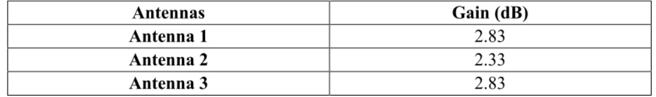
By substituting the appropriate values, the gains of the antennas can be observed in Table 5.4. Table 5.4 Gain of each antenna at 2.44 GHz
Antennas Gain (dB)
Antenna 1 2.83
Antenna 2 2.33
Antenna 3 2.83
22
5.5.3 VSWR
Voltage standing wave ratio is the ratio of input power to the reflected power. It is responsible to provide the information of power reflected from the antenna. S-parameter or return loss is also known as reflection coefficient.
Let reflection coefficient be ‘Γ’. Then, VSWR is given by VSWR = 1 +|Γ|
1 −|Γ| 0 ≤ Γ < 1 (5.13)
From (5.13), it is evident that the minimum value that can be attained is ‘1’, i.e., when the reflection coefficient is ‘0’, which is possible only when the load was perfectly matched and thereby no reflected wave. However, in practice the reflection coefficient is never ‘0’. The intention of any engineer is to design an antenna with a low reflection coefficient as shown in Fig. 5.4. The increase in VSWR results in damage of source/transmitter. Besides, it also effects the data being transmitted. An existence of interference between the power reflected and the power being transmitted yields in reduction of reliability of data transfer [20].
Fig. 5.7 Reflection coefficient versus frequency (simulated in FEKO).
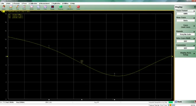
VSWR versus frequency plots of fabricated antenna are shown in Fig. 5.8, Fig. 5.9 and Fig. 5.10 acquired from the Anritsu ShockLine network analyser. Notice that Fig. 5.7. shows reflection coefficient whereas Fig. 5.8, Fig. 5.9 and Fig. 5.10 are plotted in regard to VSWR. A significant change in reflection coefficient was observed from the one simulated to the realised antennas.
23
Fig. 5.8 VSWR versus frequency – Antenna 1: Network Analyser.
24
Fig. 5.10 VSWR versus frequency – Antenna 3: Network Analyser.
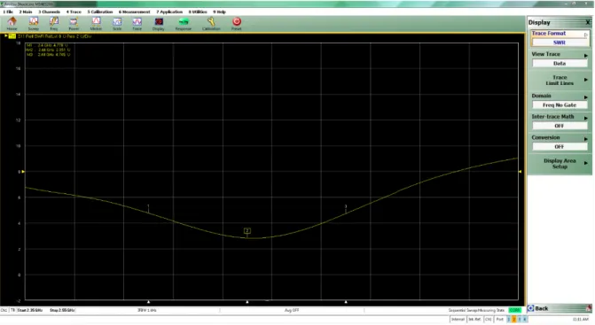
The VSWR obtained was far from the desired one. Hence, an optimization of the antennas was necessary, which was implemented by varying
the length of antennas with the copper tape as shown in Fig. 5.11.
The reduction in VSWR achieved for Antenna 1, Antenna 2 and Antenna 3 are shown in Fig. 5.12, Fig. 5.13 and Fig. 5.14, respectively.
Fig. 5.11 Optimization - Copper Tape.
25
Fig. 5.13 VSWR versus frequency – Optimized Antenna 2: Network Analyser.
Fig. 5.14 VSWR versus frequency – Optimized Antenna 3: Network Analyser.
A significant reduction in VSWR was observed, thereby the reflection coefficient and the reflected power also got reduced [21]. The variation in the VSWR, reflection coefficient and reflected power for the three antennas, before and after optimization are examined in Table 5.5.
26
Table 5.5 VSWR, reflection coefficient and reflected power before and after optimization
Frequency Antenna 1 Antenna 2 Antenna 3
VSWR 𝚪 Reflected Power (%) VSWR 𝚪 Reflected Power (%) VSWR 𝚪 Reflected Power (%) Before Optimization 2.40 GHz 8.889 0.80 63.6 9.944 0.82 66.8 7.298 0.76 57.6 2.44 GHz 5.209 0.68 46.0 6.354 0.73 53.0 4.137 0.61 37.3 2.48 GHz 3.167 0.52 27.0 3.443 0.55 30.2 3.612 0.57 32.1 After Optimization 2.40 GHz 3.365 0.54 29.4 5.433 0.69 47.5 4.778 0.65 42.8 2.44 GHz 2.98 0.5 24.7 3.325 0.54 28.9 2.851 0.48 23.1 2.48 GHz 5.598 0.7 48.6 5.517 0.69 48.0 4.745 0.65 42.5 5.5.4 Impedance
The opposition offered to current in a circuit when voltage is applied is known as impedance. In other words, impedance is a combination of resistance and reactance. Impedance consists of both real and imaginary parts. The real part of impedance represents the concrete resistance offered that helps to radiate the power from the antenna or absorb power from space with respect to its state of configuration, i.e., either transmitter or receiver, whereas the imaginary part of impedance represents the power that is stored in the near-field that is not radiated [16], [22].
There are two types of impedances namely self-impedance and mutual-impedance. Driving impedance of the antenna is either self-impedance alone when there are no obstacles/sources near to the antenna or a combination of self-impedance and mutual-impedance in their presence.
27
It is a largely accepted truth that maximum power transfer takes place when the input impedance of the antenna is conjugate to the input impedance of the circuit connected to the antenna. Additionally, the impedance of the antenna will vary with a variation in frequency. An accurate conjugate is desired to make the imaginary part to zero and thereby attaining a transmission of maximum power, however, in practice an accurate conjugate could not be attained. The impedance was measured at different frequencies for three antennas and were plotted on Smith charts as shown in Fig. 5.15, Fig. 5.16 and Fig. 5.17, respectively.
Fig. 5.16 Impedance measurements of Antenna 2 at frequencies 2.40 GHz, 2.44 GHz and 2.48 GHz.
28
Table 5.6 Frequency versus impedance
Frequency Antenna 1 Impedance (𝛀) Antenna 2 Antenna 3 2.40 GHz 62.338 - 𝑗 71.062 49.425 - 𝑗 95.055 39.731 - 𝑗 76.369
2.44 GHz 75.504 - 𝑗 65.537 58.527 - 𝑗 67.741 47.103 - 𝑗 53.004
2.48 GHz 33.914 - 𝑗 78.567 33.559 - 𝑗 77.151 30.622 - 𝑗 64.709
The negative sign of the reactance observed in Table 5.6 can be related to the capacitive reactance. The capacitive reactance is due to the presence of residue of solder flux on the circuit board. The capacitive reactance produced was in the order of Femtofarads and can be measured using microstrip directional coupler [23]. Fig. 5.18 shows the solder flux used for coaxial feeding input on all the realised antennas.
29
Chapter 6
Path Loss Model
The reduction in power density of the electromagnetic signals is known as path loss. Several parameters such as reflection, refraction, scattering, diffraction, environmental conditions, propagation medium, etc. effects path loss. Several path loss models were established to predict the signal strength at a distance away from the transmitter.
Free space path loss is estimated using the Friis transmission equation, in an ideal case where neither obstacles nor other sources are considered between the transmitter and the receiver. Satellite communications and microwave links usually undergo such free space path loss.
Friis Transmission Equation:
𝑃𝑟(𝑑) = 𝑃𝑡 𝐺𝑡𝐺𝑟𝜆2 (4𝜋)2𝑑2 = 𝑃𝑡 𝐺𝑡𝐺𝑟( 𝑐 4𝜋 𝑓𝑐𝑑) 2 (6.1)
𝑃𝑟(𝑑) is the received power [𝑊]
𝑃𝑡 is the transmitted power [𝑊]
𝐺𝑡 is the gain of transmitting antenna
𝐺𝑟 is the gain of receiving antenna
𝜆 is the wavelength [𝑚]
𝑑 is the separation between transmitter and receiver in meters [𝑚] 𝑓𝑐 is the carrier frequency [𝐻𝑧]
𝑐 is the speed of light [𝑚 𝑠⁄ ]
The gains of the antennas, 𝐺𝑡 and 𝐺𝑟 are dimensionless and a value of ‘1’ is considered if the
antennas are isotropic (radiates equally in all directions). If the antennas are non-isotropic, then the gains of the antennas may vary with units like dBi (gain in decibels w.r.t. isotropic antenna), dBd (gain in decibels w.r.t. dipole antenna), dBm (gain in decibels w.r.t. milliwatt (mW)), etc. From (6.1), it is evident that the received power reduces as the square of the distance increases between the transmitter and receiver.
Path loss is defined as the difference between transmitted power to effective transmitted power and the received power which is usually calculated in decibels (dB) as:
𝑃𝐿(𝑑𝐵) = 10 log𝑃𝑡 𝑃𝑟 = −10 log [ 𝐺𝑡𝐺𝑟𝜆2 (4𝜋)2𝑑2] (6.2) or 𝑃𝐿(𝑑𝐵) = 10 log𝑃𝑡 𝑃𝑟 = −10 log [ 𝜆2 (4𝜋)2𝑑2] (6.3)
Free space path loss can be calculated with either (6.2) or (6.3) with the knowledge of the type of antennas used. Equation (6.2) can be used in the scenarios when the antennas have gains
30
greater than unity and (6.3) can be used when the antennas used are isotropic antennas i.e., the antennas have unity gain.
Different path loss models were established via analytical and empirical form of approaches. Amongst these two approaches, the empirical models have approached nearly accurate results and are being used in several real-time scenarios [15].
6.1 Simulation on WinProp
WinProp is a software suite that helps to simulate an indoor electromagnetic wave propagation scenario for calculating path loss, power and field strength. Two scenarios were simulated using WinProp in this thesis.
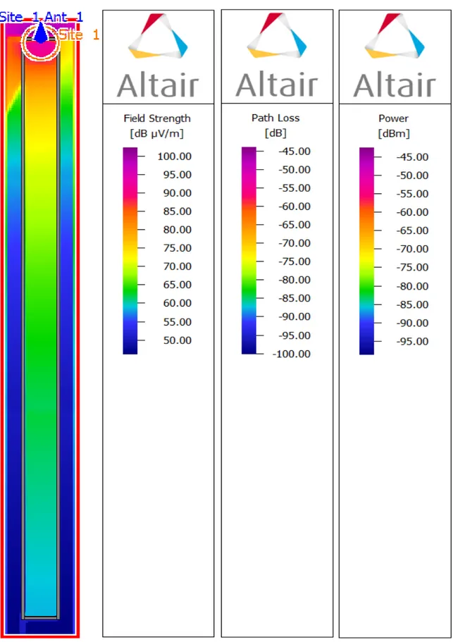
Scenario A
The path loss was estimated in a narrow corridor of cellar as shown in Fig. 6.1. The dimensions of the corridor were 30m, 1.7m and 2m. The material properties used for creating the indoor database in WallMan software tool are concrete (thickness: 20 cm) and wood (thickness: 10 cm). Walls were drawn using the concrete material properties whereas doors were drawn using wood material properties. An opening at one end of the corridor was provided using the subdivision namely, hole in the surrounding wall.
The antenna was placed in the desired position (centre of the short-edge in the corridor) by importing the above created indoor database in ProMan. Data was acquired from the designed antenna from FEKO, which is required for loading the antenna properties and the dominant path model. Henceforth, path loss, power and field strength are calculated as shown in Fig. 6.2. From Fig. 6.2., it is evident that the path loss increases, whereas power and field strength decrease as the distance of separation between the transmitting antenna and receiving antenna increases.
Fig. 6.1. Narrow corridor in cellar drawn in WallMan (Scenario A).
31
32
Scenario B
The path loss was estimated in the office premises as shown in Fig. 6.3. The office premises contain several partitions and the model was complicated with discontinuous dimensions 30m, 9m (1.5m from 20m in length) and 3m. Glass was used to construct a few partitions (height: 2m) and doors (3m). The material properties used for the model are concrete (thickness: 20 cm) and glass (thickness: 10 cm). Walls were drawn with concrete material properties and holes in the walls were created by using the option, hole in the surrounding wall.
The antenna was placed at one of the corners in the structure and this new indoor database was imported onto ProMan software tool. The acquired data from FEKO and dominant path model were used in ProMan. Henceforth, path loss, power and field strength were measured as shown in Fig. 6.4. From Fig. 6.4., it is evident that the path loss increases, whereas power and field strength decrease as the distance of separation between the transmitting antenna and receiving antenna increases.
33
34
6.2 Verification
The RSSI measurements were acquired for each scenario to verify the simulations in WinProp. To perform the RSSI measurements, a special setup with a transmitter and receiver is required.
Receiver
The receiver shown in Fig. 6.5 was rigged up as follows:
• A system running on Windows OS equipped with putty software was connected to the AXIS camera via a LAN cable.
• Power supply was given to the camera.
• An SSH connection was established between Putty and the camera.
• The Bluetooth and RSSI of the camera were enabled using appropriate commands.
Fig. 6.5. Putty running in Windows OS connected to the camera.
Transmitter
The transmitter shown in Fig. 6.6 was rigged up as follows:
• An appropriate code for advertising the packets has been loaded into the nRF52 DK using Keil µVision and powered.
• The fabricated antenna is connected to the nRF52 DK with coupling of two connectors namely standard SMA cable (Murata part no. MXHS83QE3000) and IPEX MHFI to SMA(F) Bulkhead Straight connector with SMA male to SMA male adapter as an interface.
• Precautions must be taken as to not bend the cable too much, to avoid spurious radiations from the cable.
35
Fig. 6.6. nRF52 DK connected to fabricated antenna via the cables/connectors.
Subsequently, the transmitter and the receiver must be aligned such that there is a LOS (Line-of-Sight) between both the antennas. The transmitter stops advertising the packets, if once a Bluetooth connection was established between the transmitter and receiver. Hence precautions must be taken to avoid this situation, since the RSSI values can be obtained only while the transmitter advertises the packets.
The setup was ready and measuring the RSSI values can be initiated by Putty. A mean of five values was considered taking into account the randomness of a wireless link. The receiver was kept stationary and the RSSI values were acquired by moving the transmitter away from the receiver in the order of 5 meters for the three patch antennas.
36
Scenario A
As mentioned in Section 6.1., the RSSI values were measured in the narrow corridor shown in Fig. 6.7.
Fig. 6.7. RSSI measurements taken in narrow corridor in cellar.
Table 6.1 RSSI values measured for the three antennas in Scenario A
Distance (Meters) Antenna 1 (dB) Antenna 2 (dB) Antenna 3 (dB)
5 -64 -65 -68 10 -69 -70 -71 15 -74 -75 -75 20 -79 -80 -79 25 -80 -81 -80 30 -81 -82 -81
The curve-fitting tool in MATLAB was used to construct the best fit for the obtained data points in Table 6.1 using linear method. Fig. 6.8, Fig. 6.9 and Fig. 6.10 show the best fitted curves for Antenna 1, Antenna 2 and Antenna 3, respectively. The path loss exponents for the three antennas are 0.7, 0.7 and 0.54.
37
Fig. 6.8 RSSI (dB) versus distance (m) of Antenna 1 in Scenario A.
Fig. 6.9 RSSI (dB) versus distance (m) of Antenna 2 in Scenario A.
In Scenario A, the width of the structures is very narrow compared to the length. Hence, the structure is approximated to behave like a waveguide. Multiple reflections appear from the walls of the structure. This results in concentration of the signal power in the direction of the receiver. The reduction in path loss was the countereffect.
38
Fig. 6.10 RSSI (dB) versus distance (m) of Antenna 3 in Scenario A.
Scenario B
As mentioned in Section 6.1, the RSSI values were measured in the office premises as shown in Fig. 6.11. Two different cases, one being the line-of-sight (LOS) and other being non-line-of-sight (NLOS) were considered in the office premises.
39
Line-of-Sight
Table 6.2 RSSI values measured in line-of-sight for the three antennas in Scenario B
Distance (Meters) Antenna 1 (dB) Antenna 2 (dB) Antenna 3 (dB)
5 -64 -65 -64 10 -72 -74 -72 15 -73 -75 -74 20 -79 -81 -77 25 -80 -83 -79 30 -78 -85 -81
The curve-fitting tool in MATLAB was used to construct the best fit for the obtained data points in Table 6.2 using linear method. Fig. 6.12, Fig. 6.13 and Fig. 6.14 show the best fit of data points for Antenna 1, Antenna 2 and Antenna 3, respectively. The path loss exponents for the three antennas are 0.57, 0.76 and 0.62.
40
Fig. 6.13 RSSI (dB) versus distance (m) of Antenna 2 in Scenario B (LOS).
41
Non-Line-of-Sight
Table - 6.3 RSSI values measured in non-line-of-sight for the three antennas in Scenario B
Distance (Meters) Antenna 1 (dB) Antenna 2 (dB) Antenna 3 (dB)
5 -73 -75 -71 10 -73 -76 -75 15 -75 -78 -73 20 -83 -85 -78 25 -81 -87 -80 30 -83 -89 -82
The curve-fitting tool in MATLAB was used to construct the best fit for the obtained data points in the Table. 6.3 using linear method. Fig. 6.15, Fig. 6.16 and Fig. 6.17 show the best fit of data points for Antenna 1, Antenna 2 and Antenna 3. The path loss exponents for the three antennas are 0.46, 0.62 and 0.42.
42
Fig. 6.16 RSSI (dB) versus distance (m) of Antenna 2 in Scenario B (NLOS).
43
Losses
The signal energy is reduced due to the loss introduced by cables / connectors. An insertion loss of 5 dB was introduced, i.e., more than half of the signal power is attenuated before it reaches the antenna for radiation.
Table 6.4 Loss introduced due to cables/connectors to connect nRF52 DK and antenna
Cables/Connectors Loss (dB)
SWF Switch Connector 0.1 [24] SMA/Male to SMA/Male Adapter 0.5 Conn MEAS Probe for SWD/SWF Conn 1.0 [12] IPEX MHFI to SMA(F) Bulkhead Straight Connector 3.1 to 3.4 [25]
44
Chapter 7
PIR Sensor
Passive infrared (PIR) sensors also known as pyroelectric or IR motion sensors are less expensive, compact, low-power and user friendly. Hence, they are often used in most home appliances for detecting or sensing the movement of a human. All bodies radiate a gaugeable level of IR radiation. The heat of the body is directly proportional to the radiation intensity, i.e., if a body holds much heat then its radiation intensity is high and vice versa [26].
The motion sensor helps to detect a motion (of human), but cannot specify the number of persons present or how far the human is away from the sensor. They are rigged up with a pyroelectric sensor which contain large electric fields and have the capability to generate a temporary voltage upon sensing heat or cold [26].
7.1. PIR Sensor Functionality
As can be seen from Fig. 7.1, the PIR sensor contains two slots that are capable to sense the IR radiations. The range of detecting area depends on the sensitivity of the sensor. These two slots are responsible for detecting the motion of a human which are made of different materials, yet detect the same amount of radiation. Due to the change in the temperature detected on both slots while a human moving will create a differential voltage which is responsible for sensing the movement of a human [27].
45
The sensitivity, breadth and range of the PIR sensors can also be varied with the lenses used. The lenses used are convex lenses as shown in Fig. 7.2, capable of condensing a large area into a small area, thereby increasing the capability of the PIR sensor [27].
Fig. 7.2. Fresnel lens and plano convex lens [27].
Fig. 7.3. Passing of light through Fresnel lenses [27].
Since the convex lenses occupy more space and increase weight, Fresnel lenses are used. Capturing of light through Fresnel lenses can be seen in Fig. 7.3. The sensing through PIR sensor can be enhanced further by increasing the slots. The two slots can be further divided by making partitions in the lens [27].
46
7.2. PIR sensor integration with nRF52 DK
This sensor was integrated into the nRF52 DK using appropriate circuitry. The circuitry includes a couple of resistors, a transistor, a LED and a PIR sensor. The functioning of the PIR sensor was acknowledged with LED. PIR sensor can be powered with a battery, however in this thesis, the power required for the PIR sensor was drawn from the nRF52 DK.
Fig. 7.4. Integration of PIR sensor with nRF52 DK.
It can be seen from Fig. 7.4, the red line is connected from 𝑉𝑐𝑐 of the circuitry to the 𝑉𝑑𝑑 of
nRF52 DK, similarly the ground (Black line), thereby powering the PIR sensor. The yellow line is connected to the 19th pin of nRF52 DK, for switching the PIR sensor wirelessly from
the camera, as this was the intention of the thesis.
The on-board LEDs are ACTIVE LOW. If the logic is HIGH when the voltage is LOW at a pin is known as ACTIVE LOW since it is active in spite of its LOW voltage.
Working Case 1
The Case 1 is when LED – 3 is OFF. The on-board LED is ACTIVE LOW, and the voltage at the pin is HIGH. The voltage at pin 19 reflects the voltage at the drain of the NPN transistor (2N7000). To switch ON the transistor, sufficient voltage must be applied across the GATE of NPN transistor.
47
The current conducted due to the high voltage at 19th pin, passes through the LED connected
externally, when the transistor is OFF or open circuited. If the transistor is ON, the conducted current passes through the transistor and reaches ground, thereby resisting the current to pass through the LED.
The OUT of PIR sensor was connected to the GATE terminal. A PIR sensor will conduct current upon detecting a motion that would switch ON or OFF the transistor which would switch OFF or ON the external LED connected to the circuitry.
Case 2
The Case 2 is when LED – 3 is ON. The on-board LED is ACTIVE LOW, and the voltage at the pin is LOW. The voltage at pin 19 reflects the voltage at the drain of the NPN transistor (2N7000). The LOW voltage at the 19th pin will switch OFF the external LED connected to the
circuitry.
Even though, the transistor switches ON and OFF due to the current conducted at the GATE of the transistor, the LED will switch OFF since the voltage at the 19th pin is LOW.
48
Chapter 8
Prototype System
A prototype is an early stage in the process of building a final product. All the essential features in the final product will be available in a working prototype. Intensive tests are conducted in this stage to identify and enhance the fragile parts of the prototype. Numerous iterations will be carried out before proceeding further towards a final product.
8.1 Design and Implementation
In this thesis, a prototype of the Blue Cool Connectivity Box was built. The design process of the prototype can be given explicitly as follows:
• Configuration of AXIS Camera • Configuration of nRF52 DK
• Connection of designed antenna to nRF52 DK • PIR sensor integration with nRF52 DK
Configuration of AXIS Camera
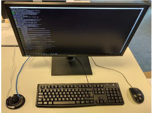
The AXIS camera was powered and connected to the system via a LAN cable as shown in Fig. 8.1. A connection was made between the network camera and a system (computer) with an SSH connection (network protocol) via Putty through port 22. The command bluetoothctl can be seen from Fig. 8.2. This command was used to establish a connection between the AXIS Camera and nRF52 DK.
Fig. 8.1. AXIS camera connected to the system via LAN cable and power cord.
The firmware used in the camera was modified for accessing Bluetooth. The commands used in Fig. 8.2 were pertaining to the firmware used and a few commands may not be accessible upon using other versions.
49
Fig. 8.2. bluetoothctl commands used for setting up connection between camera and nRF52 DK.
The attributes visible in Fig. 8.2, help to serve several purposes. However, only the vendor specific characteristic attribute highlighted was used to send write commands to nRF52 DK.
50
Configuration of nRF52 DK
As described in Section 3.2.2, the on-board LEDs and buttons were programmable. Among 4 LEDs available, 3 LEDs were programmed as follows:
• When nRF52 DK broadcasts advertising packets to establish a connection with a central device or master, LED-1 was programmed to switch ON.
• Upon establishment of a connection with another device, LED-1 was programmed to switch OFF indicating an end for broadcasting of packets whereas LED-2 was programmed to switch ON indicating the existence of a connection.
• The functionality of the LEDs will swap upon termination of the connection.
• LED-3 was programmed to switch ON upon receiving a write command of ‘01’ (Anything greater than ‘00’) via LED characteristic (0x1525).
• LED-3 was programmed to switch OFF upon receiving a write command of ‘00’ via LED characteristic (0x1525).
The code programmed fulfilling all the above conditions was loaded to nRF52 DK with Keil µVision upon powering it.
Connection of designed antenna to nRF52 DK
The designed antenna was connected to nRF52 DK with cables/adapters/connectors. The cables/adapters/connectors used were as follows:
• IPEX MHFI to SMA(F) Bulkhead Straight connector as shown in Fig. 8.3(a) • SMA male to SMA male adapter as shown in Fig. 8.3(b)
• Standard SMA cable (Murata part no. MXHS83QE3000) as shown in Fig. 8.3(c) • Connector of SWF type (Murata part no. MM8130-2600) as shown in Fig. 8.3(d) • Molex Micro-coaxial connector as shown in Fig. 8.3(e)
The cables shown in Fig. 8.3 (a) and (c) have SMA (F) connectors and an adapter SMA (M) to SMA (M) as shown in Fig. 8.3 (b) was used as an intermediate converter. The connector SWF type was used on nRF52 DK board capable for internal switching. Molex micro-coaxial connector as shown in Fig. 8.3 (e), was soldered to the antenna and the IPEX MHFI to SMA(F) Bulkhead Straight connector terminates on the antenna. Standard SMA cable terminates on the SWF type connector as shown in Fig. 8.3 (d) of nRF52 DK. Nearly, a loss of 5 dB was introduced due to the presence of these cables/adapters/connectors.
51
Fig. 8.3. The cables/adapters/connectors used between antenna and nRF52 DK.
(a) (b)
(c) (d)