Router Architecture for Junction Based
Source Routing: Design and FPGA
Prototyping
Muhammad Awais Aslam
G e t_ a rb 2 m o d _ n Input Port Junction&Resource Control Header_Modifier RTR_n Put_n Data_in_N Req_buf2mod_n D a ta _ b u f2 ju n _ n Data_buf2mod_n
Path Table Arbiter
G e t_ P T 2 ju n _ n N e w a d d _ P T 2 ju n _ n Path Table Desadd_PTA2PT D e s a d d _ ju n 2 P T A _ N R e q _ b u f2 ju n _ n Data_jun2mod_n Req_jun2mod_n R e q _ ju n 2 P T A _ n Arbiter &Control S e l_ E S e l_ S S e l_ W S e l_ N S e l_ R PUT_N-S-W-E-R RTR_N-S-W-E-R R e q _ m 2 a -s -w -e -r D a ta _ m o d 2 a rb _ n R e q _ m o d 2 a rb _ n Cross Bar D_m2b_s D_m2b_w D_m2b_e D a ta _ m o d 2 b a r_ N G e t_ a 2 m -s -w -e -r G e t_ p ta 2 ju n _ s -w -e -r D a d d _ ju n 2 p ta -s -w -e -r Read_PTA2PT Readover_PTA2PT Accept_mod2jun_n Get_mod2buf_n Dataout_S Dataout_N Dataout_E Dataout_R Dataout_w D_m2b_R D a ta _ m o d 2 a rb R e q _ j2 p ta -s -w -e -r I/O interfa ce DSP Memo ry Proces sor Graphic controller I/O interfa ce Nios II FPGA Video Rceive r Proces sor FPGA Audio Recei ver DSP Video tranmi tter Audio Trans miter Memo ry J Video Transmi tter Audio Transmi tter DSP I/O Interfa ce FPGA Memo ry Nios II Video Recei ver Graphic Controller
MASTER THESIS 2011
Electrical Engineering: Specialisation in Embedded
Systems
Router Architecture for Junction Based
Source Routing: Design and FPGA
Prototyping
Muhammad Awais Aslam
This exam work has been carried out at the School of Engineering in Jönköping in the subject area Electronics. The work is a part of the two-year Master of Science programme.
The authors take full responsibility for opinions, conclusions and findings presented.
Supervisor: Shashi Kumar and Rickard Holsmark Examiner: Shashi Kumar
Scope: 30 credits (D-level) Date:
Abstract
The increase in the number of cores that can be integrated on a single chip has forced the designer to use computer network concepts for design of System on Chip (SoC). This idea led to development of Network on Chip (NoC) to deal with more cores on a single chip. NoC has three main parts, namely routers, link and network interface through which cores are connected to NoC. Router is one of the most important parts because cores communicate with other cores through routers. One of the important tasks for a NoC designer is to design router with low latency.
Router design depends on the routing protocol and routing algorithm used. Two kinds of routing algorithms are source routing and distributed routing. In source routing, complete route information is available in Head flit while in distributed routing, routing decisions are taken inside every router on the path. Source routing has speed advantage over distributed routing because the packet itself contains the routing information. But source routing leads to overhead to store complete path information in the header of each packet. To overcome this flaw, junction based source routing has been introduced. If destination is far away from the source then first packet will go to a junction and get the new path information from the junction to the destination. Thus we need to store the path information only for a few hops in the packet header. This idea has been taken from the daily experience of train journey. In this thesis we have developed design of a router for junction based source routing. Main component of simple router includes buffering, header modification and making route decision. Router includes a table called Path Table which stores information about paths from junction to various destinations. JB router also includes, picking up the new path information from Path Table and modify the header by adding new path information.
We have developed VHDL designs of two versions of the routers for Junction Based Routing. The delay performance of routers have been analysed through simulation. A simple prototype of the router has also been implemented in Altera FPGA to find out the resource requirements of the new router designs.
Keywords
System on Chip (SoC) Network on Chip (NoC) Source routing
Distributing routing Junction Based routing Router architectures Path Table
Altera FPGA NiosII Core
Acknowledgement
First of all I am thankful to Almighty Allah, the Most Beneficent, the Most Merciful whose blessings provided me the strength to successfully complete this Master Thesis.
I would like to thank my supervisor Professor Shashi Kumar, who introduced me to the field of NoC and provided me the opportunity to work under his kind supervision. I am thankful to him for providing me with invaluable guidance throughout the thesis work. His research experience and regular meetings with motivating solutions provided me a great opportunity to learn many things throughout the thesis. I am grateful and feel proud to work under the supervision of one of the founders of Network on Chip (NoC) paradigm.
I thank Rickard Holsmark for his supervision and support. I appreciate his time and cooperation that helped me in enhancing my thesis design.
I would like to thank Alf Johansson, Master program coordinator, for being helpful and caring throughout the Master program.
Last but not least, I am very thankful to my parents for their motivation during my difficult hours and support throughout my life.
Table of Contents
1
Introduction ... 1
1.1 SYSTEM ON CHIP ... 1
1.2 NETWORK ON CHIP ... 1
1.3 IMPORTANT ISSUES IN NOC BASED DESIGN ... 2
1.4 GOALS,SCOPE AND TASKS OF THE THESIS ... 3
1.5 THESIS LAYOUT ... 4
2
Theoretical Background ... 5
2.1 NOCCONCEPT ... 5
2.1.1 Core to Core Connections ... 5
2.1.2 Bus Based Connections ... 6
2.1.3 Router Based Connections ... 7
2.2 NOCTERMINOLOGIES AND SWITCHING TECHNIQUES ... 8
2.3 COMPONENTS OF NOCARCHITECTURE ... 9
2.4 ROUTING ALGORITHM ... 10
2.4.1 Distributed vs. Source routing ... 10
2.4.2 Junction Based Routing (JBR) ... 11
2.4.3 Comparison of Header Format ... 13
2.5 ROUTER ARCHITECTURE ... 14
2.5.1 Functionality of router ... 14
2.5.2 Input buffer ... 14
2.5.3 Cross Bar Switch ... 15
2.5.4 Arbitration and Control ... 15
2.6 HANDSHAKING PROTOCOL... 16
2.7 GAISLER’S TWO PROCESS METHOD ... 17
2.8 PROTOTYPE OF DESIGN ... 18
2.8.1 FPGA Technology ... 18
2.8.2 FPGA Prototyping Design Flow ... 19
3
Router Design Options ... 21
3.1 HARDWARE ROUTER ... 21
3.1.1 Architecture ... 21
3.2 NETWORK PROCESSOR AND SOFTWARE ROUTER ... 23
3.3 TABLE BASED ROUTER ... 25
3.4 COMPARISON ... 26
4
Router Design for Junction Based Routing (JBR) ... 27
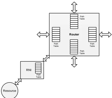
4.1 PATH TABLE STORAGE OPTIONS ... 28
4.1.1 Path Table in router for each Input Port and one Path Table in RNI ... 28
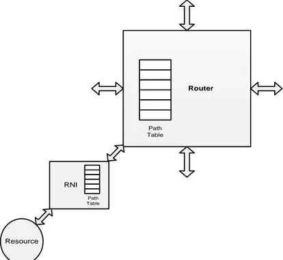
4.1.2 Common Path Table for all Input Ports in router and one Path Table in RNI ... 29
4.1.3 Common Path Table in RNI ... 30
4.1.4 Only One Path Table in router ... 31
4.2 PACKET FORMAT ... 32
4.2.1 Flit format ... 33
4.3 DESIGN OVERVIEW ... 35
4.4 ROUTER DESIGN DETAILS ... 37
4.4.1 Input Handler (IH) ... 37
4.4.2 Path Table Arbiter Component (PTAC) ... 43
4.4.4 Cross Bar ... 49
5
VHDL Modeling, Simulation and Results... 51
5.1 TEST RESULTS ... 52
5.1.1 Testing with Zero load ... 52
5.1.2 Testing with load and no output port conflict ... 53
5.1.3 Testing with output port conflict ... 55
5.2 IMPROVED DESIGN ... 56
5.3 RESULTS ... 57
5.3.1 Testing with Zero load ... 57
5.3.2 Testing with no output port conflict ... 58
5.3.3 Testing with output port conflict ... 60
6
FPGA Prototyping ... 64
6.1 PROTOTYPE RESULT ... 66
7
Conclusions ... 70
7.1 SUMMARY OF CONTRIBUTION ... 70
7.1.1 Path Table Options ... 70
7.1.2 Router Design, Modeling and Prototyping ... 70
7.2 LIMITATION AND FUTURE WORK ... 71
7.2.1 Path Table Compression ... 71
7.2.2 Virtual Channel in Router ... 71
7.2.3 Enhanced Pipelining Technique ... 71
7.2.4 Multiple FPGA Board for Prototyping ... 71
8
References ... 72
List of Figures
FIGURE 1.1: NETWORK ON CHIP ... 2
FIGURE 2.1: CORE TO CORE BASED CONNECTION ... 5
FIGURE 2.2: BUS BASED COMMUNICATION INTERFACE ... 6
FIGURE 2.3: A 3X3 ROUTER BASED NETWORK ... 7
FIGURE 2.4: NOC COMPONENTS ...10
FIGURE 2.5: A 7X7 JUNCTION BASED NETWORK ON CHIP BASED SYSTEM ...12
FIGURE 2.6: FORMAT OF HEAD FLIT IN SOURCE ROUTING ...13
FIGURE 2.7: FORMAT OF HEAD FLIT IN JUNCTION BASED ROUTING ...13
FIGURE 2.8: ROUTER ARCHITECTURE ...15
FIGURE 2.9: HANDSHAKING PROTOCOL BETWEEN SENDER AND RECEIVER ...16
FIGURE 2.10: GENERIC TWO PROCESS CIRCUIT [14] ...17
FIGURE 2.11: CYCLONE II BLOCK DIAGRAM [12] ...18
FIGURE 2.12: QUARTUSII DESIGN FLOW [15] ...20
FIGURE 3.1: A TYPICAL NOC ROUTER ...22
FIGURE 3.2: MULTIPLE PC BASED ARCHITECTURE [11] ...24
FIGURE 3.3: LATENCY/FLEXIBILITY VS. PERFORMANCE GRAPH ...25
FIGURE 4.1: SEPARATE PATH TABLE IN ROUTER FOR EACH INPUT PORT AND ONE PATH TABLE IN RNI...29
FIGURE 4.2: COMMON PATH TABLE FOR ALL INPUT PORTS IN ROUTER AND ONE PATH TABLE IN RNI...30
FIGURE 4.3: COMMON PATH TABLE IN RNI ...31
FIGURE 4.4: ONLY ONE PATH TABLE IN ROUTER ...31
FIGURE 4.5: FORMAT OF HEAD FLIT IN JUNCTION BASED ROUTING ...34
FIGURE 4.6: FORMAT OF BODY FLIT IN JUNCTION BASED ROUTING ...34
FIGURE 4.7: FORMAT OF END FLIT IN JUNCTION BASED ROUTING ...34
FIGURE 4.8: FORMAT OF FULL FLIT IN JUNCTION BASED ROUTING ...35
FIGURE 4.9: BLOCK DIAGRAM OF JUNCTION BASED ROUTER ...35
FIGURE 4.10: ARCHITECTURE OF INPUT PORT ...38
FIGURE 4.11: CIRCULAR MEMORY BUFFER ...39
FIGURE 4.12: REGISTER CHAIN FOR IMPLEMENTING BUFFER ...39
FIGURE 4.13: HEADER MODIFIER ...40
FIGURE 4.14: JUNCTION & RESOURCE CONTROL...42
FIGURE 4.15: PATH TABLE ARBITER ...44
FIGURE 4.16: HIERARCHICAL FSM ...45
FIGURE 4.17: TABLE COMPONENT ...45
FIGURE 4.19: DIRECTION DECODING ...48
FIGURE 4.20: CROSS BAR ...50
FIGURE 4.21: ARCHITECTURE OF JUNCTION BASED ROUTER ...50
FIGURE 5.1: ROUTER DELAY FROM INPUT PORT TO OUTPUT PORT ...51
FIGURE 5.2: ITERATIVE CIRCUIT IMPLEMENTATION IN ARBITER & CONTROL ...57
FIGURE 5.3: SIMULATION RESULTS WHEN JB OR RB IS ‘0’ ...61
FIGURE 5.4: SIMULATION RESULTS WHEN JB OR RB IS ‘1’ ...62
FIGURE 6.1: HARDWARE ARCHITECTURE OF THE SYSTEM ...64
FIGURE 6.2: QUARTUS II ARCHITECTURE ...65
FIGURE 6.3: FLOW CHART DIAGRAM OF THE DESIGN AND TEST PROCESS ...67
List of Tables
TABLE 2.1: CYCLONE II FAMILY OVERVIEW [19] ...19
TABLE 3.1: LATENCY OF DIFFERENT ROUTERS ...24
TABLE 3.2: COMPARISON BETWEEN DIFFERENT ROUTER DESIGN OPTIONS ...26
TABLE 4.1: COMPARISON BETWEEN DIFFERENT ROUTER ORGANIZATIONS ...32
TABLE 4.2: FLIT TYPES AND THEIR ENCODING...33
TABLE 4.3: DIRECTION CODES ...49
TABLE 5.1: SIMULATION RESULTS (WITHOUT LOAD) ...53
TABLE 5.2: SIMULATION RESULTS (WITHOUT OUTPUT PORT CONFLICT) ...54
TABLE 5.3: SIMULATION RESULTS (WITH LOAD AND OUTPUT PORT CONFLICT) ...55
TABLE 5.4: IMPROVED RESULTS (WITHOUT LOAD) ...58
TABLE 5.5: IMPROVED RESULTS (WITH LOAD AND NO OUTPUT PORT CONFLICT) ...59
TABLE 5.6: IMPROVED RESULTS (WITH LOAD AND OUTPUT PORT CONFLICT) ...60
TABLE 6.1: FPGA IMPLEMENTATION RESULTS OF JBR ROUTER ...68
List of Abbreviations
RNI Resource Network Interface IHC Input Handler Component PTA Path Table Arbiter
PT Path Table
JTAG Joint Test Access Group
UART Universal Asynchronous Receiver Transmitter RTR Ready to Receive
NoC Network on Chip SoC System on Chip
ASIC application Specific Integrated Circuit IP Intellectual Property
LE Logic Elements
PIO Parallel Input/Output JB Junction Bit
RB Resource Bit
J&R Junction & Resource A&C Arbiter & Control
VHDL Very High Speed integrated circuit Hardware Description Language SOPC System on Programmable Chip
FPGA Field Programmable Gate Array FSM Finite State Machine
LUT Look Up Table
CLB Configurable Logic Block
1 Introduction
New developments are necessary in every field, especially in technology, to improve quality of life. As we know this is the era of research and there is research in every field of life. In electronic, more emphasis is on how to reduce the chip area, its cost and how to develop a product in short interval of time. Integrating a complete system on a single chip is known as “System on Chip”. A lot of work has been done in this field. A regular increase in the number of transistors on a single chip has opened new fields and makes it possible to develop more complex systems on a single chip. Due to the increased complexity, there was a need of introducing a platform which makes it easy to integrate new component on a single chip with reduced complexity. In the last few years, a platform has been introduced name as Network on Chip (NOC). NOC has made it easy to develop systems with large number of cores on single chip in an easy way.
1.1 System on Chip
According to the Moore’s law the number of transistors doubles almost every 18 months [9]. All this is possible due to advancements in CMOS technology and it is easy to achieve billion of transistor on single chip. Due to the increase of numbers of transistors on a single chip, it is possible to develop more complex systems on a single silicon chip. The whole system is integrated in the using components which are called IP cores. These IP cores are directly connected to communicate with each other. These IP cores can be reused in different systems. These cores can be processors, I/O controllers, memory blocks, DSPs, video controller and many others. Increase in number of cores will increase interconnects complexity on the chip.
Earlier there were direct connections or busses used to connect cores. A bus is a shared resource which limits the number of cores connected to bus and it is difficult for multiple cores to communicate at the same time. More resources connected to bus also slow down the communication. This is one of the main problems in current SoCs. Problem with direct connections is that they have low scalability. To overcome these problems there was need of some new idea, which had been proposed a decade before. Next section will explain that idea.
1.2 Network on Chip
Interconnects and shared bus problems made researchers to think about a platform which can give an easy way to integrate new cores as well as old cores by following a protocol. On-chip packet-switched networks have been proposed as a solution for the problem of global interconnects in deep submicron VLSI Systems-on-Chip (SoC) [4]. A decade before an idea was introduced to use the networking concepts in SoC. Instead of using direct connection among cores, switches are introduced inside the chips for communication between the cores. One of the advantages of using switches is to make the SoC more scalable and flexible. Resources can share data with each other regardless they are connected
directly or not. Reuse of components (cores) has become easier than ever. These features have increased the importance of NoC in the field of electronics.
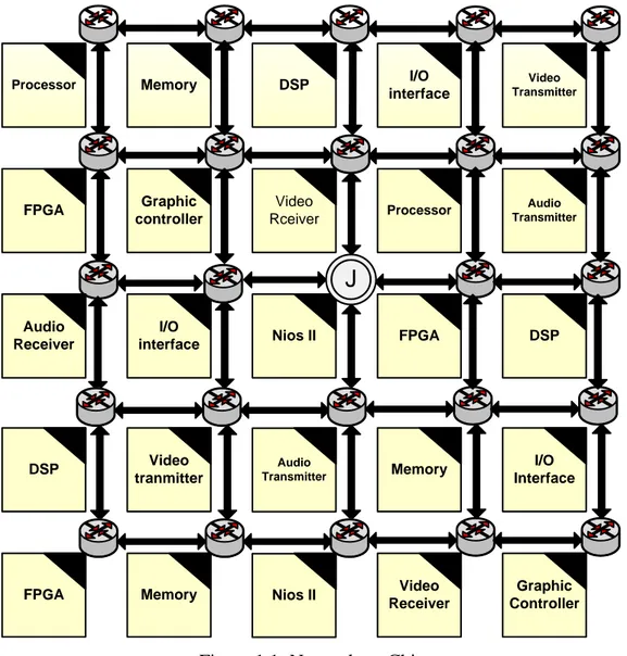
A typical Network on Chip platform with mesh topology is shown in Figure 1.1.
Audio Transmitter Nios II I/O interface DSP Memory Processor Graphic controller I/O
interface Nios II FPGA
Video Rceiver Processor FPGA Audio Receiver DSP Video tranmitter Memory
J
Video Transmitter Audio Transmitter DSP I/O InterfaceFPGA Memory Video
Receiver
Graphic Controller
J
Figure 1.1: Network on Chip
A Core is connected to the router through RNI. RNI is the interface between router and the core. Core sends packet to the router through RNI, and from router it is send to the other routers or core depending on the destination. In literature, different NoC architectures have been proposed by the researchers [6] [7] [8].
1.3 Important Issues in NoC based Design
NoC design deals with many important issues. First issue in NoC is topology. Topology has importance for system performance and for complexity of router design. A good topology can make the router design less complex. There are different kinds of topologies in network like mesh, torus star, ring, spidergon and
tree etc but it is found that most suitable topology for NoC is mesh topology. Routing algorithm is second issue in NoC because router design also depends on routing algorithm. There are two kind of routing algorithms called source routing and distributed routing. In source routing, path information is pre calculated and stored into packet header before sending the packet into network. The path information is stored in the form of Path Tables which can be placed either in router or in resource itself. In distributed routing, header packet only contains the destination address. Path decisions are taken inside the router by implementing routing function or by reading routing tables. Source routing has an advantage over distributed routing because path is pre-determined which make the router design simpler. But there is also a drawback in source routing. Due to packet overhead it needs more buffer size to store packet which results in more cost. To overcome this flaw junction based source routing has been introduced. The basic idea is to limit the required path information to be stored in every packet to a small number of bits. The large distance is covered by going through intermediate temporary destinations (called Junctions). Since router design depends on routing algorithm therefore we have chosen the junction based source routing for router design.
1.4 Goals, Scope and Tasks of the Thesis
Router is the most important component for design of communication backbone of a NoC system (like any other network). The design of a NoC router depends on various aspects of NoC architecture and the performance requirement. Each resource is connected to router through RNI.
In research work, goals are of great importance. Appropriate goals become cause of good research. First goal in this thesis is to design router architecture for junction based source routing. Junction based source routing needs two kind of router design: one for normal router and other for junction router. In the beginning of the thesis, the idea was to design two different routers but while analysing router design options it was decided that we will design a single router which works as normal router as well as junction router. Results are the most significant part of the research. Second goal of the thesis is to model the design in VHDL and simulate the design to evaluate its performance in various situations. The third goal was to prototype the design on Altera FPGA DE2 board and to evaluate its resource requirements.
In junction based routing, there is a need to store Path Tables in a router for new path information. This is a new issue because storing a Path Table in router makes it costly. One of the goals of the thesis was to develop a way to store a Path Table in router to make it efficient but less costly. How many copies of Path Table need to store in router to have efficient working was the question addressed? There is always trade-off between efficiency and cost to get good results. We will discuss about all possible design options and their comparison later in this thesis.
To achieve these goals, firstly specifications are made for router architecture by using systematic and modular approach. Router is divided into blocks and sub
blocks. Each block is designed using hardware description language VHDL. Each block is also simulated by using test benches in VHDL. To achieve the high performance an improved design is proposed and simulated after this. Simulation results of improved design are compared with earlier design and performance is evaluated. Since junction based router needs Path Table inside the router which uses memory to store path information. Due to increase in design complexity and Path Table, resource requirements also increase for junction based routing. Secondly, after simulation results, the design is prototyped on Altera FPGA DE2 board for cost and speed analysis. Purpose of the prototyping is to check the resources used by the router design on FPGA. Resources occupied by the router are also compared with NIOS II CPU. Design is also tested by connecting NIOS II with router to send packets to router and then receive it from the same router by NIOS II.
1.5 Thesis Layout
Detailed discussion about NoC and routing algorithms has been described in chapter 2. This chapter also includes discussion about router architecture and their specification. In the end it describes about which tools have been used for design prototyping.
Design option is an important issue in the field of electronics. It varies from place to place and depends where the system would be used. Sometimes pure hardware design is good and sometimes mixes of software and hardware design is good. Since this thesis is about router design, a detailed discussion about different kinds of routers has been described in chapter 3. In the end, a comparison is given between different kinds of router design options.
Chapter 4 describes the detailed design of router architecture which is also the area of the thesis. Different Path Table storage options are also described in this chapter.
In chapter 5, Improved router design, Simulation results obtained from first design and improved design are described in this chapter.
Prototyping results obtained from design by using Altera FPGA DE2 board are described in chapter 6. This chapter also includes the comparison of resources used by the JBR router and NIOSII on FPGA.
Chapter 7 describes the conclusion of thesis work. Future work is also described in this chapter.
2 Theoretical Background
In this chapter, theoretical background of NoC platform, routing algorithms, router architectures and prototype of design has been described. Starting from NoC, we will discuss the basic concept of NoC taking from network communication to improve SoC and after that basic component of NoC. It is important to have knowledge of network communication to work in NoC. In the end detail discussion about prototyping will be described.
2.1 NOC Concept
Before starting about NoC, we will discuss the main problem in SoC due to which NoC idea came to existence. Before 2000, SoC interconnects have not been designed as networks. Core to core connections or Bus based connections were used in SoC for communication between different cores. Due to increase in number of cores in a silicon chip has affected the salability, resource utilization and speed of communication of the cores..
2.1.1 Core to Core Connections
In 1990s in a SoC all cores were directly connected with each other. In other way we can also say that these cores have point to point interconnection with each other. If a core wants to send data to another core, it sends that data directly to the destination there is no intermediate state. There is no arbiter inside the chip which can control the communication between the cores. Communication speed is very fast between the cores because of direct connection. For small number of cores it is best to use direct connections but complexity increase with the increase of number of cores. A large number of cores need large number of I/O pins to communicate with each other which results in large routing area, as well as large number of wires. NIOS II CPU Memory PS2 Mouse Controller JTAG UART Audio VGA
Direct interconnections have following disadvantages.
Low scalability
Low routing resources utilization since connections are dedicated for each pair
Uncertainty regarding quality of signals
SoC using direction connections does not have the feature of scalability. It is difficult to add new cores in the system. Reuse of component is also a big issue for SoC. Each connection between the cores is used by self-connected cores. Other cores cannot use the same connection which reduces the utilization of routing resources. There are also no criteria to test the quality of signal as it can be uncertain because of increasing clock and changed geometry of wires which may increase the noise.
2.1.2 Bus Based Connections
In SoC while using direct interconnections, the main problem is increase in number of I/O pins as well as cost with the increase in chip area. To avoid these problems bus based interconnection has been introduced. Instead of connecting the cores directly, all cores are directly connected to the bus which behaves as the shared medium between all cores. Cores in SoC are connected to the bus through an interface. An arbiter is used to handle the communication between the cores. If any core wants to communicate with other core then it has to wait until bus is free to use and arbiter generates some control signal to handle the bus and give access to the relevant cores. A bus based communication interface between different IP is shown in the Figure 2.2.
NIOS II CPU Internal RAM PS2 Mouse Controller
JTAG UART PIO
JTAG Cosole
and Debugger Mouse VGA
In this figure, mouse controller receives the data from the mouse and sends it to the Nios II CPU through Avalon Bus or vice versa. Then CPU sends the mouse movement data to the VGA through Avalon Bus which generates the mouse cursor on the screen.
One of the advantages of using bus is scalability as compared to direct interconnections. Number of wires and I/O pins are also reduced which results in the reduction of chip area. Still there are some flaws which are described below.
Scalability reduced with increase of cores after a certain limit
Low speed
As the number of cores increased beyond the limit, it affects the performance and scalability of the system. Since all cores are sharing the same medium therefore only two cores can communicate with each other at a time. Due to arbitration and increase in length of the bus speed of communication is also decreased.
2.1.3 Router Based Connections
As it has been described above that SoC has some major problems as we increase the area of the chip. To overcome these flaws a network based platform has been introduced which is known as Network on Chip (NoC). In NoC, network related concepts are used. For example, instead of using direct connections or busses, a network of routers are used to connect cores with each other through interface known as RNI (Router to Network Interface). Data is sent from one core to other core in the form of packets through routers.
Audio Internal RAM NIOS II CPU JTAG UART JTAG Cosole
Mouse VGA PIO
PS2 Mouse Controller
NoC based systems have the following advantages.
High scalability
High performance
Low cost
One of the advantages of the NoC is high scalability as compared to the bus based systems which allows the reuse of cores. NoC based systems also have high performance, low cost and short time to market.
2.2 NoC Terminologies and Switching Techniques
In this section, we will discuss about some commonly used terminologies and switching techniques which are suitable for NoC router.
Message
A message is a real data which is sent from source to destination. It could be of a fixed size or of any variable length depending on the protocol used. A message can have many packets.
Packets
Message can be broken into different parts due to large amount of data. These fixed size parts are known as packets. Packet can move from source to destination through routers independently. Packet needs some information before sending it into the network like some control information and destination address etc. This information is attached to the packet and known as header of the packet. Rest of the packet contains the original data and also known as payload. A packet can also be divided into smaller parts known as flits.
Flit (Flow Control Digit)
Flit also called flow control digit is the smallest unit of the message which has fixed length. The storage elements in the network routers have the same length as of the flits.
Switching Techniques
Switches are used in the networks to control the flow of data and manage the right path by following some predefined protocols. Data is sent from source to destination through switches. Performance of the network is very much dependent on the switching techniques used. There are few switching techniques which are used in the networks.
Store and forward
Circuit switching
In store and forward switching technique, a complete packet is sent from one router to another. No packet can move to the next router until it is completely received by the previous router. This results in higher delay in communication. Also buffer size increases because of the complete packet storage.
In circuit switching, a physical connection is created from source to destination before starting the communication. Data travel from source to destination through these established connections and after successful transmission of data, connection is removed. This switching technique has disadvantage in the form of resource utilization which are not completely used.
In wormhole switching technique, a packet is divided into flits and sent towards the destination through routers. There are three types of flits known as Head flit, Body flit and End flit. First Head flit is sent into the network which locks the path for rest of the flits. Body flit which contains the actual data or payload follows the same path as locked by the Head flit. Body flit may be more than one depending on the size of data. End flit is sent in the end which means there are no more Body flits. End flit also unlocks the path. Since flits are moved like worm in the network that’s why it is called wormhole switching. One of the advantages of wormhole switching technique is their reduced buffer size. There is no need of buffer size equal to a complete packet.
2.3 Components of NOC Architecture
There are three main components of NoC. Resource
Resource Network Interface (RNI)
Router
Components of NoC architecture are shown in Figure 2.4. We will discuss these components one by one.
Resource
Resource is the basic component of the platform using a NoC which is sometimes called core. These cores can be processors, I/O controllers, memory blocks, DSPs, video controller, audio controllers Tx/Rx and many others. A core could be a new component manufactured by the vender or it could be the reuse of an old component. Sometimes pre-designed components are available free of cost but sometimes one needs to buy them. These pre-designed components are also known as Intellectual Property (IP).
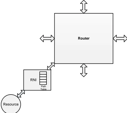
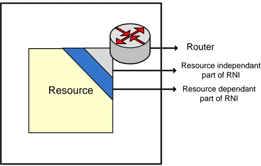
Resource Network Interface (RNI)
RNI is the second component in NoC. RNI behave as an interface between resource and router that is why it is called Resource Network Interface. Resource sends packet to the router through RNI. The RNI in NoC and network card in internet have the similar purpose. RNI is divided into two parts. One part is known as resource dependent part and other is known as resource independent
part. As it is clear from the name that resource dependent part deals with the resources while resource independent part deals with router. The purpose of resource dependent part is to receive packet from the resource, flitize the packet and send it to the router. Flitization is the process to dividing packet into flits. If there is no space in router then flits are stored in buffer in RNI and waits until router is ready to receive the flits. Similarly the purpose of resource independent part is to receive the flits from the router, deflitize it and send it to the resource. The process of converting flits into packet is known as deflitization. Flits are stored in a buffer if resource is not ready to receive the packet. Path Table can also be stored in RNI to put the path information inside the Head flit. A thesis work has already been done on RNI [5].
Resource
Router Resource independant part of RNI Resource dependant part of RNIFigure 2.4: NoC components
Router
Router is the most important component in the NoC. All resources communicate with each other through router. Purpose of the router is to receive packet from the resource and send it to another resource through router or multiple routers depending on how far is the destination. Design of the router depends on the routing algorithm used. Choice of the algorithm can make the router design simpler and less costly.
2.4 Routing Algorithm
2.4.1 Distributed vs. Source routing
Routing in NoC can be classified in many ways. But here we will discuss two way classifications. Routing can be classified into source routing and distributed routing. These will be discussed one by one.
Source routing
In source routing, path followed by the flit from source to destination is predetermined. All the path information from source to destination is stored in the Head flit. Router takes decision by looking at the Head flit. There is no extra logic used to calculate the path inside the router. Path information is calculated inside the source before sending flits into the network. For this purpose Path Tables are stored inside the source core or resource network interface (RNI). These Path Tables contain the complete path information for a specific destination in the network. Path information is calculated by applying routing algorithms [10]. When a core wants to send the packet into the network, it stores path information into packet header.
Distributed routing
Distributed routing can be static/deterministic or adaptive. In static routing the path between a pair is fixed. In adaptive routing there are multiple paths and actual path taken depends on network condition. In distributed routing, routing logic is implemented inside the router because there is no information about the path inside the header packet. Only destination address and some control bits are added in header packet. Each router in the network has information about the neighbouring router which is stored in the form of tables. Design for router is complex in this routing technique because extra hardware is needed for routing logic and bigger memories are required to store the routing tables.
2.4.2 Junction Based Routing (JBR)
Source routing is very suitable for NoC due to its deterministic nature. But there is need of change in this algorithm due to its packet overhead. Drawback in this algorithm is that header of the packet contains all information of the path from source to destination which means it needs more buffer size to store the packet. A large buffer size means it increases the cost of the router.
A new algorithm called Junction Based Source Routing has been developed to overcome this flaw. The basic idea is to limit the required path information to be stored in every packet to a small number of bits (corresponding to only a few hops). The large distance is covered by going through intermediate temporary destinations (called Junctions) such that sub-paths (from source to a junction, junction to another junction, and junction to the destination) are always smaller than or equal to a maximum hop count. If a packet needs to go through a junction (or many junctions) the source just appends path information from source to the junction. On reaching the junction, the packet picks up path information to reach the destination (or another junction) from this junction [18].
Real Life Example
Idea of junction based source routing resembles with real life train system. In train system it is very difficult to build big platform at every station from where you can find any train for any city. Development cost is increased for each big platform in every city and for some small cities resource utilization is not efficient like big
cities. To overcome this problem junctions are build in big cities. Purpose of the Junction is to give facility to passengers for the small cities or the places which are far away from the small cities. Suppose a passenger wants to go to a city or village which is not far away from its home city then he can go by direct train. But if he wants to go to a village or city which is not near then first he has to go to the Junction from there he will change the train for destination. If destination is is still far away then there might be possibility to change the train twice through another Junction. Using this idea make the source routing more efficient in term of cost.
Audio Transmitter Nios II I/O interface DSP Memory Processor Graphic controller I/O
interface Nios II FPGA
Video Rceiver Processor FPGA Audio Receiver DSP Video tranmitter Memory Video Transmitter Audio Transmitter DSP I/O Interface
FPGA Memory Video
Receiver Graphic Controller I/O interface Processor FPGA Memory Video Transmitter Audio Transmitter DSP I/O Interface Video Receiver Graphic Controller I/O interface DSP Memory Processor Graphic controller Video Rceiver Processor FPGA Video Transmitter Audio Transmitter I/O interface Processor Video Transmitter Audio Transmitter J1 D3 D1 J2 D2
Figure 2.5: A 7X7 Junction Based Network on Chip based system
A packet reaching a Junction may or may not use path information stored in the Junction. There are three distinct cases:
i. If the destination of the packet is the resource connected to the Junction itself, then it should be routed to the resource through RNI.
ii. If the destination is not very far and the packet header has enough information to reach the destination, then the router forwards the packet just looking at the relevant field in the header.
iii. If the destination is far, then the Junction will be the intermediate destination. This will be clear from the relevant field in the header. In this case, Junction modifies the path information in the packet header for onward journey to the destination, if possible otherwise to another junction as intermediate destination.
A 7X7 Junction Based routing NoC with three different distinct cases is shown in Figure 2.5.
In Figure 2.5, green arrow shows the packet movement when the destination is not far away, red arrow shows the packet movement when the destination is connected to the junction and blue arrow shows the packet movement through junction when the destination is far away from source.
2.4.3 Comparison of Header Format
Head flit format of source routing and junction based routing is shown in the Figures 2.6 and 2.7 respectively.
Flit Type 26 bits 2 bits 34 bits Path Information Source Address 6 bits
Figure 2.6: Format of Head flit in Source Routing
RB Flit
Type JB Path info Dest. Address Payload
6 bits 8 bits 16 bits 2 bits 34 bits 1bit 1bit
Figure 2.7: Format of Head flit in Junction Based Routing
Source routing and junction based source routing both are 34 bits long and have first two bits as flit type which must be “00” for Head flit. Source routing Head flit used six bits for source address which means it can carry the source address of maximum 8X8 mesh NoC. The information about source address is necessary for the destination to know where it came from. Twenty six bits are reserved for path information which carries total information from source to destination. Since there are five output ports in a router so two bits are enough for each output port
selection. It can also say that each hop needs two bits. Total 13 hops can be stored in Head flit which is enough for 7X7 mesh topology NoC. It is a big problem for larger network to reach the destination with such a limited number of hops.
Junction based routing has some extra field in the Head flit which are Resource Bit (RB), Junction Bit (JB), Destination address and payload. It does not have any source address because we have assumed that when we reach a junction to pick up path for the next segment we do not need to remember where we came from. Resource Bit (RB) is used by the resource when it needs path information from Path Table. It is not necessary for the router to work as junction. If RB is ‘1’ then flit will get the path information from the Path Table first then move towards the destination. If Resource Bit (RB) is ‘0’ then its mean Head flit already has the path information. Junction Bit (JB) is used when Head flit has to change its path information from junction router. If Junction Bit (JB) is ‘0’ then its mean Head flit contains the path information till destination. No need to change the path information because destination is not far away from the source. Sixteen bits are reserved for path information. Total eight hops are allowed from source to destination. If destination is more than eight hops then it must go to the destination through junction. Eight bits are reserved for destination address. Max of 16X16 mesh topology is allowed in the network. Rest of the six bits is used for payload. These bits can also be used for sending signals. Head flit locks the corresponding path for Body and End flits in both kind of routing.
2.5 Router Architecture
2.5.1 Functionality of router
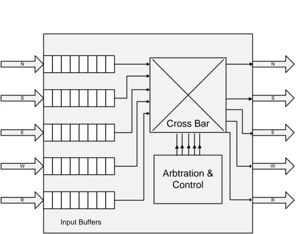
Router plays an important role in networks. Its main purpose is to receive packets from the sender, take decision by executing an algorithm and send the packet towards the destination. While going towards the destination, a packet may have to pass from several routers. Design of a router is very much depends on the routing algorithm used. A suitable routing algorithm makes the router less complex and faster. A NoC based router has the same functionality. Router architecture has three main components.
Input buffer
Cross Bar
Arbitration and Control
2.5.2 Input buffer
Input buffer is the temporary storage component. Main purpose of input buffer is to temporarily store the incoming packets if the router is busy or desire output is not empty. Input buffer is controlled by the Arbiter and Control block.
2.5.3 Cross Bar Switch
Cross Bar facilitates to connect an Input Port to any output port. Cross Bar is a combination logic which makes switching between different ports by receiving signals from Arbiter and Control block.
2.5.4 Arbitration and Control
Arbiter and Control is the most important component of the router. It behaves like its brain. All routing decisions are taken inside this component. It resolves conflicts for simultaneous requests to an output port. It also organizes the flow of packets through the router. This component is actually the implementation of routing algorithm. It controls the input buffer by sending some signals to it. When a desired output is empty then it selects the desired output by sending the selection signals to the Cross Bar and sends a control signal to the input buffer to pass through the Cross Bar to the desire output. Typical router architecture is shown in Figure 2.8. D1 D2 D3 Cross Bar Arbtration & Control D1 D2 D3 Input Buffers
Figure 2.8: Router architecture
Functionality can be implemented in many ways. Two important ways are called:
Hardware router
Software router: using general purpose processor (GPP) or application specific processor (ASP)
2.6 Handshaking Protocol
Since each router has to be connected with other routers or different resources. It is difficult for both resources and router to have same communication speed. As we know processors are software based and speed of software is slower than the speed of hardware. Therefore a protocol is necessary for the communication of different components of NoC. In our design we have used handshaking protocol to communicate between different routers and resources.
According to this protocol if any router or resource wants to send a flit to another router or resource then it will check if the buffer of next router or resource has space or it is already full. This can be checked by reading RTR (ready to receive) signal. If it is ‘1’ then its mean buffer has space to store flit but if it is ‘0’ then its mean buffer is already full and there is no space. If there is space then a Put signal is sent to the receiver side until RTR signal does not become low. Data is also sent to the receiver at the same time. After saving data receiver makes the RTR signal to low and Put signal is also become low after getting RTR signal low. After receiving low Put signal by the receiver it will check the empty space in buffer. If there is any space left in buffer RTR signal will go high which means buffer has space to store further flit.
Handshaking protocol is a simple protocol but it is a time consuming process. But it ensures that no flit will be lost during communication. There is no need of this protocol if all the components of NoC are synchronous with each other but mostly resources are not synchronous with routers or RNI. Handshaking protocol in the form of signal is shown in the Figure 2.9.
Sender Receiver RTR=1 Put=1 RTR=0 Put=0 RTR=1
2.7 Gaisler’s two process Method
The most common style for modelling a Design in VHDL is known as “Data flow” style. These kind of modelling styles are good when designs are simple but with the increase in design complexity it is difficult to read and understand the VHDL data flow code as VHDL contains a large number of concurrent statements and concurrent processes. Due to this characteristic it is difficult to guess the execution order of statements.
Due to this problem, Jiri Gaisler has introduced a new coding style to improve the readability and uniform way of encoding the algorithm. This coding style is known as Gaisler’s two process method [14]. According to this method, VHDL code consists of two concurrent processes. One process is used for combination (asynchronous) logic and the other process is used for sequential logic (Registers). Generic two process circuit is shown in the Figure 2.10.
Gaisler’s two process method is used to achieve the following goals.
To provide uniform algorithm encoding
To make abstraction level high
To improve readability
To distinguish between combinational logic and sequential logic.
To improve simulation speed
Common model for simulation and synthesis
We have used Gaisler’s two process method to design various component of our design. Combinational sequential D Q Clk r rin Q=f(D,r) rin=f(D,r) r=rin
2.8 Prototype of Design
2.8.1 FPGA Technology
In the past, Application Specific Integrated Circuit (ASIC) was used for the specific purpose designs. Due to their high cost and non-reprogrammable behavior, FPGA has become an emerging technology now a day. FPGA is an abbreviation of Field Programmable Gate Array. It can be configured or programmed on the circuit board. FPGA is a technology which is used for prototyping of different designs. Programmable logic blocks and programmable interconnects allow the FPGA to be used and re-used in many different applications. Due to their reprogrammable behavior, FPGA is more cost effective as compared to the ASIC.
FPGA consists of combinational blocks and special blocks. Combinational blocks include small number of gates and flip flops while special blocks include RAM blocks and Multipliers etc. In Xilinx, combination blocks are known as configurable logic blocks (CLB) while in Altera, it is known as Logic Blocks (LB). In this project work, we have selected Altera DE2 for prototyping of our design. Altera has different families but their basic architecture is same. A logic block consists of four input look up table (LUT) and a flip flop. The outputs of LUT and flip flop are the input of a MUX. LUT is a memory having different combination values that can implement any function of four variables. Altera cyclone II basic architecture is shown in Figure 2.11.
Different devices belonging to cyclone II family is shown in Table 2.1. It includes total number of LEs, Memory blocks, Multipliers, PLLs and I/O Pins.
Device EP2C5 EP2C8 EP2C15 EP2C20 EP2C35 EP2C50 EP2C70
LEs 4,608 8,256 14,448 18,752 33,216 50,528 68,416 M4K RAM Blocks
(4 kbits + 512 Parity Bits) 26 36 52 52 105 129 250
Embedded Memory (Kbits)
117 162 234 234 473 581 1,125
Total RAM bits
119,808 165,888 239,616 239,616 483,840 594,432 1,152,000
Embedded Multipliers 13 18 26 26 35 86 150
PLLs 2 2 4 4 4 4 4
Maximum User I/O Pins 158 182 315 315 475 450 622
Table 2.1: cyclone II Family overview [19]
2.8.2 FPGA Prototyping Design Flow
Before implementing the design on FPGA chip, it will pass through different stages. Quartus II development tool is used for this purpose which compiles the program by checking different requirements. Quartus II software design flow is shown in the Figure 2.12.
Design files are imported into Quartus II software tool which may be a VHDL files a Verilog HDL file. When we start compilation of our design then Quartus II software will analyse the design first for errors. If there is no error in the design then it will also be synthesized. Pin assignment analysis is also the part of this process. After analysis and synthesis a report of summary is created which describe the resource utilization. Quartus II will perform fitter after finishing the analysis and synthesis. Fitter perform rout and place to fit the design into the target device. After fitting a complete resource utilization comparison summary show the details. Timing analysis measures the delay along the various timing paths and verifies the performance and operation of the design [15]. After successful compilation, compiler will generate .sof/.pof files which mean design is ready to program the chip.
3 Router Design Options
For any design it is important to keep in mind about some pros and cons and their effect on the system. Router is an important component in network. Speed and cost of the network mostly depends on the router used. There are different options of router design. For example, hardware router, network processor or software router and table based router. In this chapter we will discuss these different options, compare them and try to figure out which option is the best for our router design.
3.1 Hardware Router
Router is an important component in NoC as it provides routes for the communication between different cores. A router consists of registers, switches, arbitration and control logic that collectively implement the routing and flow control function required to buffer and forward flits to their destination [1]. Most of the NoC router proposals are of hardware type. In the past, hardware based router designs have been introduced having different architectures because architecture of hardware design depends on the algorithm used. For example, router design for source routing is different from the router design for distributed routing. In source routing, complete route information is stored in the Head flit by some pre calculations. Router takes decision by looking at the path information stored in Head flit. There is no function for path computation inside the router. While in distributed routing, decision is taken inside the router. These decisions can be taken by implementing hardware functions or by looking at the routing tables stored inside the router.
Hardware based routers are used for a single purpose. Since routers are designed especially for NoC therefore the purpose of the router is to route the flit into an appropriate direction according to the routing algorithm used as describe above. Due to their single purpose characteristics, the performance of these routers is very high. These routers are also small in size. One of the disadvantages of these routers is their inflexibility. Since router is specifically design to implement an algorithm, a slight change in the routing algorithm forces the designer to rebuild the complete architecture again. These routers have very high speed because of hardware implementation as well as low cost due to their single purpose. But development cost is very high, which is the main drawback of hardware router. The idea of router architecture described in [10] has been used for this thesis to develop a junction based router. New components have been added to control the junction of the network. Developing new router architecture from scratch is time consuming process. It is better idea to reuse the previous concepts which helps to reduce the design time.
3.1.1 Architecture
The router architecture shown in Figure 3.1 is a typical NoC router. Design of a router depends on the routing algorithm used. In source routing, router receives
flits from neighboring router or from core through RNI then takes decision by looking at the Head flit and sends the flit towards the required port. In distributed routing, routing decision is taken inside the router through implemented routing functions. Routers based on source routing have simpler architecture as compared to the distributed routing based architecture because there is no need to take routing decisions inside the router. Main components in the router architecture are as follow.
Arbiter and Control
Cross Bar Input buffer N S E W R Cross Bar Arbtration & Control N S E W R Input Buffers
Figure 3.1: A typical NoC Router
3.1.1.1 Arbitration and control
This is the main component of the router architecture. It is not wrong if we say it is the brain of the router. All decisions are taken inside this component. Main responsibility of Arbiter and Control is to control the communication between different input ports to different output ports. It also resolves the contention problem between the inputs ports which desire the same output port by giving them priority. It selects the output port by sending signal to Cross Bar. Locking and unlocking of path is also its responsibility. It locks the path after passing the Head flit and unlocks the path after sending the End flit.
3.1.1.2 Cross Bar
Cross Bar is the collection of multiplexers through which flits are sent to the outside of the router. The purpose of the Cross Bar is to receive signals from the Arbiter and Control to select the output direction line for the relevant input port. A flit is transferred from an input port buffer to an output through Cross Bar. 3.1.1.3 Input Buffer
The purpose of input buffer is to store flits coming from different routers or coming from the core. Input buffers could be register based or memory based depending on the size of the buffer. If buffer size is small then register based buffers are good but if buffer size is large then it is good to use memory based buffers. When input buffer receives signal from Arbiter and Control then it sends flit to the Cross Bar.
3.2 Network Processor and Software Router
Second option for designing a router will be to use a general purpose processor (GPP) or an application specific processor especially suitable for router functionality. In both cases router functionality is implemented by writing software for this processor. This application specific processor is also called Network processor [11]. Because of their application specific nature, the network processors have new instruction set as compared to GPP. GPP are more flexible than network processors because they can be used for any purpose by changing the software but these processors have very high latency and require large area. On the other hand, network processors have low latency and needs less area as compared to GPP because of their application specific nature. These network processors and software routers are very costly because they need large memory to store the software for specific applications.
NoC is based on computer networks ideas. These ideas are always used to improve NoC’s performance. Network processors are specific purpose processors and therefore these processors are used to implement routers in computer networks. These processors have also become part of NoC router design and therefore these processors are also known as Micro-Network Processor (µNP). A thesis work related to µNP has been described in [11]. Processor based on µNP has its own instruction set.
Example of Instructions
µNP has almost all the instructions of GPP but also has some special instructions for routing functions. An example of a routing instruction is QRT (Quick route). This instruction set the data path in µNP to move a flit from an input port to an output port [11]. There are also instructions for assigning priorities to various input ports as well as locking or unlocking output port for multi-flit packets. µNP is a multi-threaded processor architecture as shown in the Figure 3.2. One program thread handles one input port therefore µNP has five threads (PC counters) for ports and one thread (PC counter) for general configuration and control.
PC_C Processor’s Data Path Program memory PC_N PC_S PC_W PC_E PC_R Active Active_C Active_N Active_S Active_W Active_E Active_R P C S e l
Figure 3.2: Multiple PC based architecture [11]
Latency
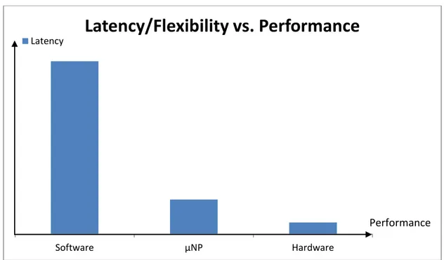
Performance of a router depends on the latency of the packet. Performance is high if latency of the packet is low. Latency of the packet means that time taken by the packet from its entrance into the router until the time of its leaving the router. Performance of the hardware router is high as compared to the software router and µNP. Similarly performance of µNP is better than software routers. Reason is that hardware routers are faster than the µNP and software routers and therefore they have low latency and high performance. µNP are not good as hardware router but they are better than software routers. µNP has latency higher than hardware router but very less than software routers and their performance is also very good as compared to the software routers. Latency of different routers in terms of clock cycles is given in the following Table 3.1.
Routers Latency (clock cycles)
Hardware 2-5
Software >100
µNP < 20
Latency vs. performance graph is shown in Figure 3.3. The purpose of the graph is only to highlight the large differences in latencies of various router implementations.
Flexibility
Hardware routers are not flexible like software routers or µNP. Because if there is any change in routing algorithm, all the design will be changed which leads to design a new one. Software routers and µNP both are software based which gives a great flexibility. Any change in routing algorithm can be fixed by changing only software. Software routers are more flexible than µNP because software routers are General Purpose (GPP) which gives more flexibility to deal with different kind of programs. On the other hand µNP are application specific which restrict them to deal with only routing algorithms. Flexibility vs. performance graph is shown in Figure 3.3.
Figure 3.3: Latency/Flexibility vs. Performance graph
3.3 Table Based Router
Third option for router design is table based router. These routers are similar to hardware router. The only difference is that routing functions are implemented through tables. In other way we can say that routers take decision by looking at tables. These routers are fast like hardware routers because no software programs are used inside the router. Therefore these routers are not flexible like network processors and software routers but still they are better than hardware router in term of flexibility because routing algorithms are implemented through tables. Any change in routing algorithm causes to change the table information only. These routers need large memories to store routing algorithm. Due to this reason,
Software µNP Hardware
Latency/Flexibility vs. Performance
Latency
table based routers are very costly. Still they have low latency because of hardware used. But altogether the performance of these routers is very good.
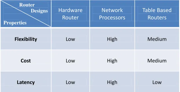
3.4 Comparison
A comparison between all three router design options is shown in Table 3.2.
Router Designs Properties
Hardware
Router
Network
Processors
Table Based
Routers
Flexibility Low High Medium
Cost Low High Medium
Latency Low High Low
4 Router Design for Junction Based
Routing (JBR)
Source routing is very suitable for NoC platforms and has many advantages over distributed routing algorithms [1] [2]. But there is a drawback in this algorithm that header of the packet contains all information of the path from source to destination which means it needs more buffer size to store the packet which results in more cost.
A new algorithm called Junction Based Source Routing has been developed to overcome this flaw. The basic idea is to limit the required path information to be stored in every packet to a small number of bits (corresponding to only a few hops). The large distance is covered by going through intermediate temporary destinations (called Junctions) such that sub-paths (from source to a junction, junction to another junction, and junction to the destination) are always smaller than or equal to a maximum hop count. If a packet needs to go through a junction (or many junctions) the source just appends path information from source to the junction. On reaching the junction, the packet picks up path information to reach the destination (or another junction) from this junction.
Router is the most important component for design of communication back bone of a NoC system (like any other network). The design of a NoC router depends on various aspects of NoC architecture and the performance requirement. A NoC employing junction based routing will have two types of router designs: one for the Normal Router and the other for the Junctions. The Junction Router must contain path information, in tables, to reach any destination. There are various possibilities of implementing these tables, either in the router itself, in the resource network interface (RNI) or in the resource (core). A packet reaching a junction may or may not use path information stored in the Junction. There are three distinct cases:
i. If the destination of the packet is the resource connected to the Junction itself, then it should be routed to the resource through RNI.
ii. If the destination is not very far and the packet header has enough information to reach the destination, then the router forwards the packet just by looking at the relevant field in the header.
iii. If the destination is far, then the junction will be the intermediate destination. This will be clear from the relevant field in the header. In this case, Junction modifies the path information in the packet header for onward journey to the destination, if possible otherwise to another junction as intermediate destination.
This chapter deals with the different router organizations having different Path Table storage options and design of the suitable hardware router. There are several Path Table storage options which give the different router organizations.
![Figure 2.11: Cyclone II block diagram [12]](https://thumb-eu.123doks.com/thumbv2/5dokorg/4567133.116737/29.892.177.720.678.1058/figure-cyclone-ii-block-diagram.webp)
![Figure 3.2: Multiple PC based architecture [11]](https://thumb-eu.123doks.com/thumbv2/5dokorg/4567133.116737/35.892.177.737.107.512/figure-multiple-pc-based-architecture.webp)