Contents lists available atScienceDirect
Microelectronics Reliability
journal homepage:www.elsevier.com/locate/microrelE
ffect of PCB cracks on thermal cycling reliability of passive microelectronic
components with single-grained solder joints
Saeed Akbari
⁎, Andreas Lövberg, Per-Erik Tegehall, Klas Brinkfeldt, Dag Andersson
RISE Research Institutes of Sweden, Box 104, SE-431 22 Mölndal, Sweden
A R T I C L E I N F O
Keywords: Lead-free soldering PCB cracking Anisotropy of tin grains Passive components Finite element modelling
A B S T R A C T
Lead-free tin-based solder joints often have a single-grained structure with random orientation and highly an-isotropic properties. These alloys are typically stiffer than lead-based solders, hence transfer more stress to printed circuit boards (PCBs) during thermal cycling. This may lead to cracking of the PCB laminate close to the solder joints, which could increase the PCBflexibility, alleviate strain on the solder joints, and thereby enhance the solder fatigue life. If this happens during accelerated thermal cycling it may result in overestimating the lifetime of solder joints infield conditions. In this study, the grain structure of SAC305 solder joints connecting ceramic resistors to PCBs was studied using polarized light microscopy and was found to be mostly single-grained. After thermal cycling, cracks were observed in the PCB under the solder joints. These cracks were likely formed at the early stages of thermal cycling prior to damage initiation in the solder. Afinite element model incorporating temperature-dependant anisotropic thermal and mechanical properties of single-grained solder joints is developed to study these observations in detail. The model is able to predict the location of damage initiation in the PCB and the solder joints of ceramic resistors with reasonable accuracy. It also shows that the PCB cracks of even very small lengths may significantly reduce accumulated creep strain and creep work in the solder joints. The proposed model is also able to evaluate the influence of solder anisotropy on damage evolution in the neighbouring (opposite) solder joints of a ceramic resistor.
1. Introduction
Thermo-mechanical fatigue of solder joints arising from mismatch in material properties between component, solder, and printed circuit board (PCB) is a major reliability issue in microelectronics assemblies [1–5]. Fatigue life of solder joints is often studied using accelerated thermal cycling tests which employ higher temperature ranges and faster ramp rates than those found infield conditions [6–8]. Also,finite element simulations can complement the experimental observations by providing more insights into mechanisms governing damage initiation and propagation in solder joints [9–11].
Grain morphology of lead-free solder alloys significantly affects damage evolution and failure under thermal cycling and needs to be investigated thoroughly to enhance the accuracy of solder joints' life prediction models. Previous studies on solidification in different tin-based solder joints have shown that they are mostly single-grained [12,13]. It has also been shown that the grains have nearly random orientation [14–16]. The randomness of the grain orientations of ad-jacent joints cause each solder joint to undergo a unique stress and strain state. Numerous studies have shown that for a ball grid array
(BGA) component, the joint with the maximum damage which failsfirst is not necessarily located at the position of the highest strain due to the global CTE mismatch (normally the point with the maximum distance from the neutral point or under the edge of the chip) [12,13,17]. This is a consequence of random orientation of the grains in single-grained solder joints with highly orientation-dependant, i.e. anisotropic, prop-erties that generates stresses and strain states varying among neigh-bouring joints.
In addition, the transition to lead-free solder alloys has increased the risk of cracking of plated through-holes (PTHs) during soldering, because the reflow temperature of lead-free alloys is higher than leaded solders [18]. This raises the thermal-mechanical stresses induced in the reflow process on the PTHs. Therefore, PCB laminates with high glass transition temperature (Tg) and low coefficient of thermal expansion (CTE) have been developed to withstand lead-free soldering and to generate low stress on the PTHs [19]. The high Tgand low CTE are achieved by using a resin with a high degree of cross-linking and a high content of inorganicfillers. This results in a laminate with a high elastic modulus but also a laminate that is more brittle than traditional low Tg laminates [20,21]. The higher elastic modulus of laminates will result
https://doi.org/10.1016/j.microrel.2019.01.006
Received 26 October 2018; Received in revised form 21 December 2018; Accepted 5 January 2019 ⁎Corresponding author.
E-mail address:saeed.akbari@ri.se(S. Akbari).
0026-2714/ © 2019 The Authors. Published by Elsevier Ltd. This is an open access article under the CC BY license (http://creativecommons.org/licenses/BY/4.0/).
in higher stress levels both in the solder joints and in the PCB laminate during thermal cycling. In addition, since lead-free solders are stiffer than leaded solders, they apply more stresses to the PCB.
The highest thermo-mechanical stress that solder joints will be ex-posed to will occur during the cooling phase after soldering. Hence, PCB cracks may form early in the soldering process. Even very small cracks in the PCB initiated during soldering can change the dominant failure mode from fatigue cracking of the solder joints to PCB cracking [22]. In fact, it has been shown that pre-stress on PCB prior to a thermal cycling test may cause latent damages in the PCB which cannot be observed as cracks in cross-sections, but nevertheless increase the risk for PCB cracking in a subsequent thermal cycling test [23].
A PCB provides the mechanical support and electrical connection for various electronic components assembled on it. It is typically a la-minated polymeric composite consisting of an epoxy resin matrix bonding woven bundles of glass fibres. Similar to other laminated composites the mechanical properties of a PCB are highly anisotropic. The in-plane stiffness and tensile strength of PCBs are much larger than the out-of-plane stiffness and tensile strength. In other words, PCBs are much stronger in fibre direction than in the transverse direction (normal to the PCB). It has been shown that the transverse tensile strength is usually of the same order of magnitude as that of the epoxy resin bonding the glassfibres [24].
The fatigue life of solder joints is predicted from accelerated thermal cycling test results by using acceleration factors to extrapolate life in field conditions. This is based on the assumption that the failure me-chanisms in both test andfield conditions are similar. This assumption may be wrong, since PCB cracking is more likely to occur under test conditions because thermal cycling parameters used in tests are nor-mally harsher than those found under typical field conditions. Therefore, the partial inconsistency of the failure mechanisms and the role of PCB cracking to reduce strain in solder joints may result in an overestimation of solder fatigue life obtained from accelerated testing [13,25].
PCB cracking has already been reported for lead-free BGA packages. Tegehall and Wetter [13] detected PCB cracking for three types of BGA packages assembled on a 1.6 mm thick PCB with SAC305 solder joints, which were subsequently thermally cycled between −40 °C and +125 °C. It was shown that the formation of the cracks in the PCB beneath the solder joints improves the thermal fatigue life of the solder joints by increasing the PCB compliance and lowering the stress and strain in the solder joints. Hagberg et al. [26] also reported that the BGA solder joints close to the PCB cracks were less damaged, con-firming that PCB cracking is a crucial parameter in thermal cycling reliability of BGA packages.
While research on thermal cycling reliability of single-grained solder joints has been mostly focused on area array components, the present study investigates this effect for ceramic resistors. Polarized light microscopy is used to study the grain structure of SAC305 solder joints connecting ceramic resistors to PCBs, and UV light is used to detect cracks in the PCB laminate. To explain the experimental ob-servations of PCB cracking and solder failure, afinite element model is developed to study the effect of random orientation of the two opposite solder joints of a ceramic resistor on the formation of cracks in the PCB, and the subsequent effect of PCB cracking on damage evolution in solder joints under thermal cycling. Accumulated creep strain and creep work are the two parameters used to quantify damage evolution in the solder joints. It is shown that the damage reduction in solder joints due to PCB cracking is proportional to the crack length.
2. Tin anisotropic properties
Most lead-free solder alloys used in electronics contain at least 95% tin to facilitate soldering at temperatures tolerable to various parts of electronic assemblies [14]. When solidifying in the soldering process, the tin forms β-Sn. As shown in Fig. 1, β-Sn properties are highly
orientation and temperature dependant. Interestingly, both elastic modulus and CTE are greatest in [001] direction (along the c-axis). The CTE in [100] and [010] directions (along the a-axis and b-axis) is about half of that in the [001] direction [27]. This ratio remains constant for different temperatures. Although the CTE peanut-shaped distribution uniformly expands in all directions from−45 °C to 135 °C, the elastic modulus distribution becomes more anisotropic with temperature in-crease. The elastic modulus along the c-axis is almost three times larger than that along a- and b-axes at−45 °C. This ratio constantly increases with temperature.
After solidification, lead-free solder joints can take three different grain structures: single grained (SG), cyclic twinned grained (CTG), and interlaced twinned grained (ITG) structure. An individual joint can also have a mixture of CTG and ITG structures. The grain structure depends on various manufacturing parameters such as joint size, surfacefinish on soldered surfaces, and cooling rate during soldering [28]. Previous studies have shown that lead-free solder joints to BGAs are often single-grained [13,25,29–31], because these joints usually undercool 20–80 °C and solidify in a single nucleation event. Moreover, since the single-grained solder joints are highly anisotropic, their orientation sig-nificantly affects the solder stress and strain distribution under different thermal and mechanical loadings [13].
Following the colour scale proposed in [12] and assuming random grain orientation, the probabilities of various c-axis orientations (from 0° to 90°) are depicted inFig. 2withfive different colours. Each colour shows an interval of 18°. On the two extremes, there exist red and blue joints. A joint with c-axis almost parallel to the board is referred to as a red joint, while a joint with c-axis almost perpendicular to the board is referred to as a blue joint.Fig. 2indicates that the probability of a red joint is about six times higher than a blue joint.
In surface mount microelectronic assemblies with multi-joint con-figurations such as resistors and BGAs, interaction of neighbouring single-grained solder joints with different orientations produces stress and strain states unique to each joint and complicates lifetime predic-tions. Stress and strain levels during temperature changes depend on the relative mismatch in thermomechanical properties between com-ponent, solder, and board, which is a function of the orientation of the single-grained solder joints. For instance, since the CTE of the PCB parallel to the board is about 15 ppm, for a single-grained solder joint the local mismatch in the CTE between the solder joint and the board is maximum when the c-axis is parallel to the board (red joint), and minimum when the c-axis is perpendicular to the board (blue joint).
The alternating tensile and compressive stresses and strains in single-grained solder joints during thermal cycling could influence the stress and strain state in component and PCB laminate. Therefore, random orientation of single-grained solder joints is a key parameter in damage initiation and propagation both in the component and in the board. Finite element analysis is a strong tool that enables detailed study of various parameters affecting solder damage, and prediction of the locations of damage initiation in the component and the PCB.
3. Experimental method
Zero-ohm ceramic resistors 1206 (CR1206) were soldered to a six-layers 1.6 mm thick FR4 PCB using SAC305 alloy (Sn with 3.0% Ag and 0.5% Cu). Fifty soldered resistors were split into ten test patterns. Each pattern consisted offive resistors connected in series. The dimensions of the solder lands were 2.0 × 1.1 mm and the distance between the solder lands was 1.9 mm. The thickness of the stencil used for printing solder paste on the solder lands was 0.127 mm. The PCB boards were produced using a laminate with a Tgof 180 °C, which is almost 30–40 °C higher than the Tgof typical PCBs used for leaded soldering. As men-tioned inIntroduction, higher Tgis achieved by adding inorganicfillers to the PCB resin. This increases the PCB stiffness (hence stress levels) and facilitates PCB cracking. The stack-up of the board is given inFig. 3. Inner layers included two signal layers and two ground layers.
The surfacefinish on the PCB was electroless nickel/immersion gold (ENIG). Thermal cycling of the test vehicles was performed between −40 °C and 100 °C with 10 min dwell time at the lower extreme and 30 min dwell time at the higher extreme. The temperature change rate wasfixed at 10 °C/min during both heating and cooling. Thus, a full thermal cycle took 68 min. The thermal cycling test was run for 6252 cycles. An event detector monitoring the daisy change resistance of the test patterns was used to record failures of the assemblies during thermal cycling.
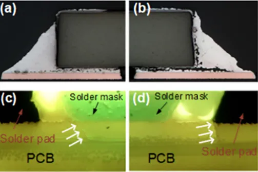
In order to detect cracks in the PCB and solder joints induced during the thermal cycling test, cross-sections of thermally cycled resistors were studied. To this end, a high-speed diamond saw was used to cut out the samples. Zestron FA was then used to clean the cut-out samples and removeflux residues. In the next step, the samples were moulded in a room-temperature curing epoxy under low-vacuum. To facilitate de-tection of very small cracks in cross-sections of the samples, a fluor-escent agent was dispensed into the moulding resin. Next, the moulded samples were cut out using the diamond blade to prepare samples. Successive grinding and polishing were performed to prepare the samples for further studies. An optical microscope with up to ×1000 magnification was used to inspect the cross-sections of the prepared samples. Polarized light was used to determine the grain structure in the solder joints and UV light to detect cracks in the PCB laminate. Cross-sections offive as-soldered CR1206 components were inspected to determine typical grain structure in non-cycled solder joints and eventual cracking in the PCB laminate after soldering.
4. Finite element modelling
Afinite element model was developed in ANSYS software to analyze the stress state in the PCB and predict damage evolution in the solder joints. The model was created using elements type Plane 183 under plane strain conditions. This assumption had negligible effect on the results, as the PCB stress and the solder creep strain changed less than 1% when plane stress conditions were assumed instead.
The stress state in the PCB in the immediate vicinity of the solder mask and the solder pad edges was calculated to assess the critical points of stress concentrations where damage can initiate in the PCB. In a structuralfinite element model, stresses at sharp corners between dissimilar materials are highly sensitive to the element size [32,33]. One possible solution to reduce mesh sensitivity is to round the sharp corners [33]. But the degree of rounding, i.e. the radius of curvature of thefillet in the sharp corners, has to be chosen arbitrarily, which may critically affect the stress results. Therefore, another solution was fol-lowed.
The primary aim of thefinite element analysis is to compare the stress and damage parameters under various conditions (e.g. the grain orientation and PCB crack length) rather than their magnitude. Following the method proposed by Grant et al. [34], the stresses were hence extracted from a small distance from the sharp corners and in-terfaces to eliminate the effects of the singular points.
Fig. 4shows a cross-section of a solder joint to a ceramic resistor and the corresponding finite element mesh. Linear-elastic material
(a)
(b)
Fig. 1. Anisotropy and temperature-dependence ofβ-Sn properties. Distribution of a) coefficient of thermal expansion and b) elastic modulus of β-Sn at −45 °C (graph bottom half) and 135 °C (graph top half). The values are in the Cartesian coordinate system for the tetragonal unit cell (top left insert) [25].
Fig. 2. The probability distribution of c-axis orientations. In a red joint, the c-axis is almost parallel to the board, while in a blue joint the c-axis is almost normal to the board [25]. (For interpretation of the references to colour in thisfigure, the reader is referred to the web version of this article.)
models were used for the various constituents of the model (Table 1), except for the solder whose elastic behavior was simulated using an anisotropic model, because the solder joints were found to be mostly single-grained. Some studies obtain solder material properties from tensile tests performed on large specimens [35,36]. However, isotropic material models are not able to predict stress and strain states in single-grained joints with random orientation. Anisotropic elastic behavior of SnAgCu solder alloys highly depend on the solder composition and the degree of precipitation hardening caused by small tin‑silver and tin‑copper intermetallic particles in the solder. However, anisotropic elastic moduli and CTEs of these alloys are not available in the litera-ture. Therefore, in this study anisotropic elastic properties and CTE of pure tin were used in thefinite element simulations [25,37].
In addition, it has been shown that the creep behavior of the lead-free solder is a strong function of the grain orientation [38,39]. For simplicity, the creep anisotropy was ignored, and the solder creep be-havior was simulated using an isotropic hyperbolic sine law:
= ⎛ ⎝ − ⎞ ⎠ dε dt A ασ Q RT [sinh( )] expn (1) whereσ, R, and T denote the stress level, the universal gas constant, and the temperature, respectively. A,α, and n are the model constants and are determined from experimental characterization data [40]. The model parameters are reported inTable 2.
PCBs used for lead-free soldering consist of relatively brittle E-glass fibres and epoxy resin [19,41], and exhibit a nearly linear stress-strain relationship in uniaxial tensile tests [42]. Therefore, maximum first principal stress was used as the failure criterion to predict damage in-itiation location in the PCBs. Since the main objective of modelling PCB cracks was to provide a basis for relative comparison of different crack
lengths, the PCB was modelled as a homogeneous material. Calculation of local values of PCB stresses requires a more detailed model including separate regions of resin and glass weaves and their respective prop-erties.
5. Results and discussion
5.1. Experimental results
In this section, the experimental results of crack and damage in-itiation in the PCB and the solder joints are presented. Also, the Fig. 3. Stack-up of the test board (solder mask not included).
(b)
PCB
Resistor
Solder
Solder Mask
Solder Pad
(a)
Fig. 4. a) Cross-section of the solder joint of the chip resistor. b) Correspondingfinite element mesh. Table 1
Properties of the resistor assembly. Coordinate y is normal to the plane of the PCB.
Material Young's modulus (GPa)
Poisson's ratio Thermal expansion coefficient (ppm/°C) Copper pad 128 0.34 17 Solder mask 3 0.30 50 Resistor 320 0.30 6.8 PCB Ex= Ez= 17.9 υxy=υyz= 0.39 αx=αz= 14.5 Ey= 7.84 υxz= 0.11 αy= 67.2 Table 2
Parameters for solder creep model [38].
A α (MPa)−1 n Q (kJ·K) R (J/(K·mol))
predictions of thefinite element simulations are presented in detail to explore the possible locations for crack initiation in the PCB and eval-uate the effect of the solder grain orientation on the PCB stress dis-tribution. The numerical results are discussed in terms of the experi-mental observations inSection 5.2.
Polarized light images of the cross-sections of the solder joints to the five as-soldered CR1206 components are shown inFig. 5. Out of the ten solder joints investigated, nine appear to have single-grained structure and only one to have CTG structure. Since cross-sections only show the grain structure in the plane of the cross-sections, it is possible that some
of the solder joints that seem to consist of only one grain may actually consist of more than one grain. Due to the randomness of the grain orientations, the two solder joints of each ceramic resistor shown in Fig. 5a possibly have different grain orientations. In addition, in-vestigation of the cross-sections using UV light showed that no cracks had formed in the PCB laminate during reflow soldering.
After thermal cycling, cross-sectioning was performed for allfive resistors from a test pattern that had failed after 5558 cycles. A com-plete crack through a solder joint was observed for one of the solder joints to all but one of the components. Cracks were also observed in the PCB close to the solder joints for allfive resistors. The cracks propa-gated vertically into the surface resin layer, then deviated after they reached the glass weave. The average crack length was 10–40 μm. PCB cracks were found in all solder joints and always on the inner side of the solder joint under the component. Fig. 6shows cross-sections of the solder joints to one of the resistors having typical cracks in the solder joints and PCB laminate. At nine of the solder joints, cracks were found close to the solder mask edge and at two of the solder joints, cracks were found close to the solder pad edge. That is, at one of the solder joints, cracks were observed both at the solder mask edge and at the solder pad edge (Fig. 7).
Since no cracks were observed in the PCB after soldering, the cracks must have formed during thermal cycling and not during soldering. The PCB cracks are assumed to form at the early stages of thermal cycling, therefore they can reduce stress in solder joint, and postpone solder cracking. If the cracks start to form in the PCB at thefinal stages of thermal cycling when creep damage has already been accumulated in the solder joint, PCB cracking will have a minor effect on solder fatigue life.
5.2. Finite element results
Thefirst principal stress distribution in the PCB near the PCB-solder mask and PCB-solder pad interfaces was calculated using the finite element model. The critical points of stress concentration and crack initiation in the PCB, located on either side of each joint close to the solder mask and solder pad edges, are indicated inFig. 8a. As explained inSection 4, for each pair of critical points the results were obtained one element away from the interface along the dashed lines shown in Fig. 8a to avoid stress singularities at sharp corners.
All solder joints were assumed to be single-grained. Various com-binations of solder grain orientations were modelled to investigate its effect on the PCB stress state. The orientation of the c-axis of each of the two solder joints of the resistor is specified with two letters. The first letter indicates the joint location on either side of the component, while the second letter shows the grain orientation. For example, Lx Ry means the c-axes of left and right joints are parallel to x and y axes, respec-tively. In all cases the c-axis of the left joint was assumed to be parallel to the x-axis, while the c-axis of the right joint was taken to be parallel to either the x, y or z axis. Therefore, three different combinations of grain orientations were investigated: Lx Rx, Lx Ry, and Lx Rz. These combinations represent extreme cases of grain orientations, and therefore extreme cases of stress states, so that other possible combi-nations fall between theses extremes.
Fig. 8shows distribution of thefirst principal stress in the PCB for various combinations of grain orientations. As expected, the stress is maximum near the sharp corners specified inFig. 8a. Regardless of the solder grain orientation, thefirst principal stress is always larger on the inner side of the joints under the components. This is consistent with the experimental observations of PCB cracking on the inner side (Fig. 6).
Evaluating the effect of neighbouring solder joints' orientation on the PCB stress is made possible by comparingFig. 8b and c. Although the orientation of the right solder joint has a negligible effect on the PCB stresses near the outer (left) side of left joint (Points A and B), it does affect the PCB stresses near the inner (right) side of left joint
(b)
(a)
Fig. 5. a) Polarized light images of cross-sections of SAC305 solder joints tofive CR1206. Out of the ten joints studied, nine were single-grained, and only one had CTG grain structure marked with a blue circle. b) Enlarged view of the solder joint with CTG structure. (For interpretation of the references to colour in thisfigure legend, the reader is referred to the web version of this article.)
(Points C and D), simply because it is located at a closer distance to the right joint and is to a larger extent affected by its grain orientation.
Out of the three grain combinations considered, the Lx Rx case generates the highest stress in the PCB, because it maximizes the mis-match of thermomechanical properties in the y direction (perpendicular to board) between the component, the solder joint, and the board, hence increases the thermal stresses generated during thermal cycling. Also, since for this grain combination, the c-axis of both joints lies in x-direction, and the CTE and Young's modulus are both maximum along the c-axis, deformation of each joint is limited by the neighbouring joint.
In addition, thefinite element simulations show that for the in-dividual joints, the solder anisotropy influences the stress state in the PCB underneath the joint. In particular, the stress at outer points is highly affected by the grain orientation. For instance, in the Lx Rx case the stress at Point G is 126% higher than the Lx Ry combination. However, as mentioned above, the stress at inner points is always larger than at outer points, and PCB cracking always starts at the inner side of the joint under the component.
These observations show that thefirst principal stress is a reliable index to predict crack initiation in the PCBs under thermal loading and could be used as an effective tool to evaluate the effect of various geometrical and mechanical properties of the microelectronic assembly on PCB cracking.
It was also of interest to investigate the effect of the size and cur-vature of the solder jointfillet, which is controlled by parameters such as stencil thickness, on the stress state in the PCB.Fig. 9 depicts the effect of solder fillet curvature on the distribution of first principal stress in the PCB near the stress concentration points of the right joint for Lx Rx combination. Concave, straight, and convex fillets were modelled using thefinite element analysis. It is observed that although thefillet curvature had a negligible effect on the stress distribution in the PCB on the inner (left) side of the joint (Points E and F inFig. 9a), it significantly affected the stress at Point G. At this point, the convex fillet produced the highest stress with a maximum that was about 75% larger than that for concavefillet. In fact, it was even higher than for the stress levels at the inner points. Therefore, fillet curvature can possibly transfer the location of crack initiation from the joint inner side Fig. 6. Cross-sections of the solder joints to a thermally cycled resistor showing a–b) cracks in the two solder joints and c–d) cracks in the PCB laminate.
to the outer side. These trends show that the PCB stress near the region of the toe of the solder jointfillet is a strong function of the fillet cur-vature so that a concave fillet results in the minimum stress con-centration.
Comparison ofFigs. 8 and 9shows that the PCB stress on the outer side of the solder joint is more influenced by the geometric and me-chanical properties of the solder joints. On the inner side of the solder joint, under the component, the geometric constraint applied by the component and the neighbouring solder joint is the major factor dom-inating the PCB stress state.
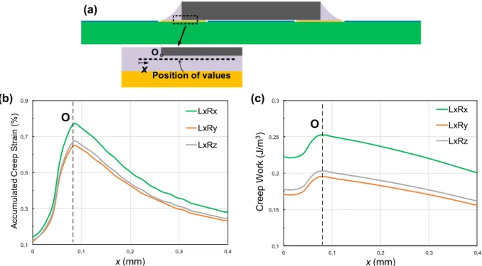
In the next step,finite element analysis was used to study the creep damage in the solder joint and the effect of PCB cracking and solder grain orientation on damage parameters. Experimental cross-sectioning showed that cracking in the solder joint started near the component corner, then propagated in different directions (Fig. 10a). The creep deformation under thermal cycling is responsible for crack initiation in the solder joints [43–45]. Therefore, accumulated creep strain and creep work were calculated for a temperature change of−40 °C–100 °C using the finite element analysis to evaluate the critical points of
damage initiation. Consistent with the experimental observations, the accumulated creep strain and creep work were both maximum near the component corner, as shown inFig. 10b and c. Since solder cracking initiates close to the component corner (Fig. 10a), and damage para-meters are maximum at this point (Fig. 10b and c), the values of ac-cumulated creep strain and creep work were calculated near this point (Point O inFig. 11a) along the dashed line. This enables quantitative comparisons of effects of grain orientation and PCB cracking.
Similar toFig. 8, three combinations of grain orientations were modelled: Lx Rx, Lx Ry, and Lx Rz. Again, the Lx Rx grain combination generated the maximum value of damage in the solder at the vicinity of Point O. In the Lx Rx combination, the c-axis of both joints is along the x-axis, parallel to the board. This means the difference in thermo-mechanical properties is maximum in the y-direction. Moreover, with temperature change, each of the two solder joints tend to expand or contract maximally in x-direction, which is limited by the deformation of the neighbouring joint in the opposite direction. This is another reason the damage generated in the solder joint is maximum for the Lx Rx combination. Overall, the trends of accumulated creep strain and
0 10 20 30 40 50 60 0 0,05 0,1 0,15 0,2 0,25 0,3 ) a P M( s s ert S l a pi c nir P t s 1 x (mm)
G
Lx Rx Lx Ry Lx RzH
0 10 20 30 40 50 60 0 0,05 0,1 0,15 0,2 0,25 0,3 ) a P M( s s ert S l a pi c nir P t s 1 x (mm)A
Lx Rx Lx Ry Lx RzB
0 10 20 30 40 50 60 0 0,05 0,1 0,15 0,2 0,25 0,3 ) a P M( s s ert S l a pi c nir P t s 1 x (mm)D
Lx Rx Lx Ry Lx RzC
0 10 20 30 40 50 60 0 0,05 0,1 0,15 0,2 0,25 0,3 ) a P M( s s ert S l a pi c nir P t s 1 x (mm)E
Lx Rx Lx Ry Lx RzF
(b)
(c)
(d)
(e)
A B C D E F G H(a)
Resistor
PCB
Solder
Position of values x Solder Mask Solder Padx
y
Fig. 8. Finite element results of the first principal stress distribution in the PCB at the vicinity of stress concentration points for a temperature change of −40 °C–100 °C. a) Schematic cross-section of resistor-solder-PCB assembly indicating eight critical points of stress concentration (Points A to H). Stresses are obtained along the dashed line specified near the stress concentration points on b) the outer (left) side of left joint (Points A and B), c) the inner (right) side of left joint (Points C and D), d) the inner (left) side of right joint (Points E and F), and e) the outer (right) side of right joint (Points G and H).
creep work are very similar, indicating either of these damage para-meters can be used to evaluate damage and failure in the solder joints. Evaluating the effect of PCB cracking on solder failure is of critical importance. For this purpose, cracks of various lengths were modelled in the PCB close to the PCB-solder pad edge, as shown inFig. 12a. The crack length (CL inFig. 12a) increased from 0.00 mm (the uncracked PCB) to 0.30 mm.
The accumulated creep strain and creep work were extracted along the dashed line inFig. 12a. Both the creep strain and the creep work decrease with the increase of crack length in the PCB, because the presence of cracks in the PCB increase the PCBflexibility. For instance, the 0.100 mm long crack reduced the accumulated creep strain and creep work by 8% and 9%, respectively. This clearly shows that PCB cracking can alleviate damage in the solder and delay its failure. Since PCB cracking may be absent infield conditions, which are milder than testing conditions, life prediction based on accelerated testing condi-tions that cause PCB cracking can overestimate the life infield condi-tions.
InFig. 12, PCB cracks of equal length were modelled on both sides of each joint. However, further simulations showed that the PCB cracks under the neighbouring joint have a negligible effect on the strain distribution and damage in the solder. Also, inFig. 12the PCB cracks were modelled near the PCB-solder pad edge. Modelling the PCB cracks near the PCB-solder mask edge changed the results by less than 3%.
A further question arises as to whether cracks on inner and outer sides of a specific joint have similar effects on damage reduction in that
joint. In order to answer this question, four different cases were mod-elled, as shown inFig. 13, which summarizes various crack location cases. The crack length was 0.10 mm in all cases. In Case 1 there was no crack in the PCB. In Case 2 and Case 3, a 0.10 mm long crack was modelled on the outer and inner sides of the joint, respectively. Finally, in Case 4 the crack was modelled on both sides. The results are shown inFig. 13. It indicates, as expected, that the inner cracks have a greater impact on damage reduction in the solder joint. On the other hand, cracks on the outer side seem to have a negligible effect on solder da-mage.
Crack initiation and propagation in the PCB increases its compliance andflexibility locally near the solder joint, hence reduces damage in solder induced by thermal stresses. The PCBflexibility can also be de-creased globally by using a thinner PCB. To show that the PCB cracking and the use of thinner PCBs have similar effects on strain reduction in the solder joints, several simulations were performed to compare the impact of these two parameters. The parameters varied in the model included the PCB thickness, and the crack length in the PCB.Fig. 14 shows that the accumulated creep strain and work in the 1.6 mm thick PCB with 50μm and 100 μm long cracks were similar to those in the 1.2 mm and 0.8 mm thick PCB with no cracks, respectively. This further confirms the effect of PCB flexibility on damage in the solder joints. 6. Conclusions
Manufacturing processes of microelectronic assemblies have 0 20 40 60 0 0,05 0,1 0,15 0,2 0,25 0,3 ) a P M( s s ert S l a pi c nir P t s 1 x (mm)
G
Concave Straight ConvexH
0 20 40 60 0 0,05 0,1 0,15 0,2 0,25 0,3 ) a P M( s s ert S l a pi c nir P t s 1 x (mm)E
Concave Straight ConvexF
(a)
(b)
Concave fillet
Straight fillet
Convex fillet
Fig. 9. Finite element results of the effect of solder fillet curvature on the first principal stress distribution in the PCB at the vicinity of the stress concentration points for Lx Rx grain combination. Stresses were calculated on a) the inner side (Points E and F), and b) outer side (Points G and H) of the right joint. The locations of these points are shown inFig. 8a.
Fig. 10. a) Cross-section of a solder joint showing the crack propagation path under thermal cycling. Distribution of b) accumulated creep strain, and c) creep work in the solder joint.
significantly changed over the past twenty years. In particular, lead-free soldering using tin-based alloys has introduced new reliability chal-lenges. Tin-based solder joints are often single-grained and exhibit highly anisotropic properties. Random orientation of the grain structure induces unique stress and strain state in each solder joint as well as in the PCB laminate. Formation of PCB cracks under single-grained solder joints is one of the issues that may have unexpected consequences on
the solder joint reliability.
In this study, CR1206 components were assembled on FR4 laminate using SAC305 solder paste. After thermal cycling, PCB cracks were observed under solder pads of the components. Since no cracks were observed in the PCB laminate after soldering, they must have formed during the thermal cycling. Such cracks can reduce the thermo-me-chanical stress on the solder joints during thermal cycling, resulting in 0,1 0,3 0,5 0,7 0,9 0 0,1 0,2 0,3 0,4 ) %( ni art S p e er C d et al u m u c c A
x (mm)
LxRx LxRy LxRz 0,1 0,15 0,2 0,25 0,3 0 0,1 0,2 0,3 0,4m/
J(
kr
o
W
p
e
er
C
3)
x (mm)
LxRx LxRy LxRz(b)
(c)
O
O
(a)
O Position of valuesx
Fig. 11. Finite element results of the accumulated creep strain and creep work distribution in the left solder joint at the vicinity of component corner. a) Schematic view of resistor-PCB assembly. The values of b) accumulated creep strain and c) creep work were extracted near Point O one element away from the solder-component interface, along the dashed line, for three different combinations of solder grain orientations.
0,1 0,15 0,2 0,25 0,3 0,35 0 0,1 0,2 0,3 0,4
m/
J(
kr
o
W
p
e
er
C
3)
x (mm)
CL= 0.00 mm CL= 0.01 mm CL= 0.05 mm CL= 0.10 mm CL= 0.20 mm CL= 0.30 mm 0,1 0,3 0,5 0,7 0,9 0 0,1 0,2 0,3 0,4 ) %( ni art S p e er C d et al u m u c c Ax (mm)
CL= 0.00 mm CL= 0.01 mm CL= 0.05 mm CL= 0.10 mm CL= 0.20 mm CL= 0.30 mm(b)
(c)
(a)
O Position of valuesx
CLO
O
Fig. 12. Effect of crack length in the PCB on the creep strain and creep work in the left solder joint. Cracks of similar length were modelled on both sides of each joint, near the PCB-solder pad interface. a) Schematic view of the assembly cross-section indicating crack modelled in the PCB. Damage parameters were extracted at the vicinity of the component corner (Point O), one element away from the solder-component interface, along the dashed line. Effects of PCB crack length on a) the accumulated creep strain and b) creep work distribution in the solder joint.
an overestimation of the fatigue life of the solder joints infield condi-tions.
A creep model was coupled with afinite element analysis to simu-late damage evolution in the solder joints influenced by PCB cracking. Modelling was performed for several grain orientation combinations. The modelling results show that the sharp corners at the edges of PCB-solder mask and PCB-PCB-solder pad interfaces generate stress concentra-tion points, and are potential sites for crack initiaconcentra-tion in the PCB.
In addition, cracks of various lengths were modelled in the PCB. The model was able to predict the location of damage initiation in the solder and PCB. It also confirmed that the presence of cracks in the PCB in-creased the PCB compliance and dein-creased the maximum accumulated creep strain and creep work in the solder joint. The effect of PCB crack length and solderfillet curvature was also studied. The modelling re-sults were in good agreement with the experimental data, confirming the effectiveness of this approach for examining damage initiation in solder joints. In this study, the PCB was modelled as a homogeneous material for relative comparison of stress levels. However, it is
heterogeneous because it has at least two phases (resin and glassfibre weave) with different properties. Accurate calculation of the PCB stress requires a more detailed model incorporating distribution offibres and resin based on their specific material properties. The heterogeneous model would also allow to simulate crack propagation at the interface offibre and resin after the crack reaches the fibre weave.
Acknowledgement
This work has been conducted within the Swedish national project "Requirements, specification and verification of environmental protec-tion and life of solder joints to components" supported by the Swedish Governmental Agency for Innovation Systems (Vinnova) under contract 2015-01420.
References
[1] C. Barbagallo, G. Malgioglio, G. Petrone, G. Cammarata, Thermal fatigue life
Case 1: no-crack Case 2: crack on outer side
Case 4: crack on both sides Case 3: crack on inner side
0,1 0,3 0,5 0,7 0,9 0 0,1 0,2 0,3 0,4 ) %( ni art S p e er C d et al u m u c c A
x (mm)
Case 1 Case 2 Case 3 Case 4Fig. 13. Effect of the location of the PCB cracks on the accumulated creep strain distribution in the solder joint. A 0.10 mm long crack was modelled in various locations in the PCB. Creep strain values were extracted one element away from the solder-component interface, along the dashed line shown inFig. 12a.
0,1 0,3 0,5 0,7 0,9 0 0,1 0,2 0,3 0,4 ) %( ni art S p e er C d et al u m u c c A
x (mm)
PCB_t=1.6 mm, CL= 0.00 mm PCB_t=1.6 mm, CL= 0.05 mm PCB_t=1.6 mm, CL= 0.10 mm PCB_t=1.2 mm, CL= 0.00 mm PCB_t=0.8 mm, CL= 0.00 mmO
0,1 0,15 0,2 0,25 0,3 0,35 0 0,1 0,2 0,3 0,4m/
J(
kr
o
W
p
e
er
C
3)
x (mm)
PCB_t=1.6 mm, CL= 0.00 mm PCB_t=1.6 mm, CL= 0.05 mm PCB_t=1.6 mm, CL= 0.10 mm PCB_t=1.2 mm, CL= 0.00 mm PCB_t=0.8 mm, CL= 0.00 mmO
(b)
(c)
(a)
O Position of valuesx
CLPCB_t
Fig. 14. Comparison of the effects of crack length in PCB and the PCB thickness on the creep strain reduction in the solder joint. a) Accumulated creep strain and b) creep work distribution in the solder joint were extracted one element away from the solder-component interface, along the dashed line.
evaluation of SnAgCu solder joints in a multi-chip power module, J. Phys. Conf. Ser. 841 (2017) 012014–012020 (IOP Publishing).
[2] L. Benabou, V. Etgens, Q.B. Tao, Finite element analysis of the effect of process-induced voids on the fatigue lifetime of a lead-free solder joint under thermal cy-cling, Microelectron. Reliab. 65 (2016) 243–254.
[3] P. Borgesen, L. Wentlent, S. Khasawneh, S. Shirazi, D. Schmitz, T. Alghoul, C. Greene, L. Yin, A mechanistic thermal fatigue model for SnAgCu solder joints, J. Electron. Mater. 47 (2018) 2526–2544.
[4] J. Chen, Y. Yin, J. Ye, Y. Wu, Investigation on fatigue behavior of single SnAgCu/ SnPb solder joint by rapid thermal cycling, Solder. Surf. Mt. Technol. 27 (2015) 76–83.
[5] R.J. Coyle, K. Sweatman, B. Arfaei, Thermal fatigue evaluation of Pb-free solder joints: results, lessons learned, and future trends, JOM 67 (2015) 2394–2415. [6] E. Dalton, G. Ren, J. Punch, M.N. Collins, Accelerated temperature cycling induced
strain and failure behaviour for BGA assemblies of third generation high Ag content Pb-free solder alloys, Mater. Des. 154 (2018) 184–191.
[7] S. Shirazi, L. Yin, S. Khasawneh, L. Wentlent, P. Borgesen, Effects of solder joint dimensions and assembly process on acceleration factors and life in thermal cycling of SnAgCu solder joints, Electronic Components and Technology Conference (ECTC), 2015 IEEE 65th, IEEE, 2015.
[8] Q. Zhou, B. Zhou, T.-K. Lee, T. Bieler, Microstructural evolution of SAC305 solder joints in wafer level chip-scale packaging (WLCSP) with continuous and interrupted accelerated thermal cycling, J. Electron. Mater. 45 (2016) 3013–3024. [9] M.M. Basit, M. Motalab, J.C. Suhling, Z. Hai, J. Evans, M.J. Bozack, P. Lall, Thermal
cycling reliability of aged PBGA assemblies-comparison of Weibull failure data and finite element model predictions, Electronic Components and Technology Conference (ECTC), 2015 IEEE 65th, IEEE, 2015.
[10] G. Elger, S.V. Kandaswamy, E. Liu, A. Hanss, M. Schmid, R. Derix, F. Conti, Analysis of solder joint reliability of high power LEDs by transient thermal testing and transientfinite element simulations, Microelectron. J. 46 (2015) 1230–1238. [11] B. Gao, F. Yang, M. Chen, Y. Chen, W. Lai, C. Liu, Thermal lifetime estimation
method of IGBT module considering solder fatigue damage feedback loop, Microelectron. Reliab. 82 (2018) 51–61.
[12] T.R. Bieler, B. Zhou, L. Blair, A. Zamiri, P. Darbandi, F. Pourboghrat, T.-K. Lee, K.-C. Liu, The role of elastic and plastic anisotropy of Sn in recrystallization and da-mage evolution during thermal cycling in SAC305 solder joints, J. Electron. Mater. 41 (2012) 283–301.
[13] P.-E. Tegehall, G. Wetter, Impact of laminate cracks under solder pads on the fa-tigue lives of ball grid array solder joints, Microelectron. Reliab. 55 (2015) 2354–2370.
[14] Z. Ma, S. Belyakov, K. Sweatman, T. Nishimura, C. Gourlay, Harnessing hetero-geneous nucleation to control tin orientations in electronic interconnections, Nat. Commun. 8 (2017) 1916.
[15] C. Gourlay, S. Belyakov, Z. Ma, J. Xian, Nucleation and growth of tin in Pb-free solder joints, JOM 67 (2015) 2383–2393.
[16] J. Xian, Z. Ma, S. Belyakov, M. Ollivier, C. Gourlay, Nucleation of tin on the Cu6Sn5 layer in electronic interconnections, Acta Mater. 123 (2017) 404–415.
[17] T.R. Bieler, H. Jiang, L.P. Lehman, T. Kirkpatrick, E.J. Cotts, B. Nandagopal, Influence of Sn grain size and orientation on the thermomechanical response and reliability of Pb-free solder joints, IEEE Trans. Compon. Packag. Technol. 31 (2008) 370–381.
[18] B. Sood, R. Sanapala, D. Das, M. Pecht, C. Huang, M. Tsai, Comparison of printed circuit board property variations in response to simulated lead-free soldering, IEEE Trans. Electron. Packag. Manuf. 33 (2010) 98–111.
[19] C.F. Coombs, Printed Circuits Handbook, McGraw-Hill, New York, 2016. [20] D. Xie, D. Shangguan, H. Kroener, Pad cratering evaluation of PCB, Proc IPC APEX
EXPO, 2006.
[21] G. Long, T. Embree, M. Mukadam, S. Parupalli, V. Vasudevan, Lead free assembly impacts on laminate material properties and“pad crater” failures, Proc IPC APEX EXPO, 2007.
[22] V. Raghavan, B. Roggeman, M. Meilunas, P. Borgesen, Effects of pre-stressing on solder joint failure by pad cratering, Proc Electronics Components Technology Conference, 2010, pp. 456–463.
[23] V. Raghavan, B. Roggeman, M. Meilunas, P. Borgesen, Effects of ‘Latent Damage’ on pad cratering: reduction in life and a potential change in failure mode, Microelectron. Reliab. 53 (2013) 303–313.
[24] L.F. Da Silva, R. Adams, Techniques to reduce the peel stresses in adhesive joints with composites, Int. J. Adhes. Adhes. 27 (2007) 227–235.
[25] A. Lövberg, P.-E. Tegehall, S. Akbari, D. Andersson, On the formation and propa-gation of laminate cracks and their influence on the fatigue lives of solder joints, Thermal, Mechanical and Multi-physics Simulation and Experiments in Microelectronics and Microsystems (EuroSimE), 2018 19th International Conference on, IEEE, 2018.
[26] J. Hagberg, J. Putaala, J. Raumanni, O. Salmela, T. Galkin, BGA interconnection reliability in mirrored module configurations, IEEE Trans. Compon. Packag. Manuf. Technol. 7 (2017) 1634–1643.
[27] J. Xian, G. Zeng, S. Belyakov, Q. Gu, K. Nogita, C. Gourlay, Anisotropic thermal expansion of Ni3Sn4, Ag3Sn, Cu3Sn, Cu6Sn5 andβSn, Intermetallics 91 (2017) 50–64.
[28] A. Lövberg, P.-E. Tegehall, G. Wetter, K. Brinkfeldt, D. Andersson, Simulations of the impact of single-grained lead-free solder joints on the reliability of ball Grid Array components, Thermal, Mechanical and Multi-physics Simulation and Experiments in Microelectronics and Microsystems (EuroSimE), 2017 18th International Conference on, IEEE, 2017.
[29] B. Arfaei, M. Anselm, F. Mutuku, E. Cotts, AREA-effect of PCB Surface Finish on Sn Grain Morphology and Thermal Fatigue Performance of Lead-free Solder Joints, SMTA International, 2014.
[30] P. Darbandi, T.R. Bieler, F. Pourboghrat, T.-k. Lee, The effect of cooling rate on grain orientation and misorientation microstructure of SAC105 solder joints before and after impact drop tests, J. Electron. Mater. 43 (2014) 2521–2529.
[31] T.-K. Lee, K.-C. Liu, T.R. Bieler, Microstructure and orientation evolution of the Sn phase as a function of position in ball grid arrays in Sn-Ag-Cu solder joints, J. Electron. Mater. 38 (2009) 2685.
[32] R. Adams, R. Atkins, J. Harris, A. Kinloch, Stress analysis and failure properties of carbon-fibre-reinforced-plastic/steel double-lap joints, J. Adhes. 20 (1986) 29–53. [33] R. Adams, J. Harris, The influence of local geometry on the strength of adhesive
joints, Int. J. Adhes. Adhes. 7 (1987) 69–80.
[34] L. Grant, R. Adams, L.F. da Silva, Experimental and numerical analysis of single-lap joints for the automotive industry, Int. J. Adhes. Adhes. 29 (2009) 405–413. [35] F. Che, W. Zhu, E.S. Poh, X. Zhang, X. Zhang, The study of mechanical properties of
Sn–Ag–Cu lead-free solders with different Ag contents and Ni doping under dif-ferent strain rates and temperatures, J. Alloys Compd. 507 (2010) 215–224. [36] P. Lall, S. Shantaram, D. Locker, High strain rate properties of SAC105 and SAC305
leadfree alloys after extended high temperature storage, J. SMTA 27 (2014) 13–27. [37] S. Park, R. Dhakal, J. Gao, Three-dimensionalfinite element analysis of
multiple-grained lead-free solder interconnects, J. Electron. Mater. 37 (2008) 1139–1147. [38] S. Mukherjee, B. Zhou, A. Dasgupta, T.R. Bieler, Mechanistic modeling of the
ani-sotropic steady state creep response of SnAgCu SINGLE Crystal, ASME 2015 International Technical Conference and Exhibition on Packaging and Integration of Electronic and Photonic Microsystems collocated with the ASME 2015 13th International Conference on Nanochannels, Microchannels, and Minichannels, American Society of Mechanical Engineers, 2015.
[39] S. Mukherjee, B. Zhou, A. Dasgupta, T.R. Bieler, Multiscale modeling of the ani-sotropic transient creep response of heterogeneous single crystal SnAgCu solder, Int. J. Plast. 78 (2016) 1–25.
[40] G. Cuddalorepatta, M. Williams, A. Dasgupta, Viscoplastic creep response and mi-crostructure of As-fabricated microscale Sn-3.0 Ag-0.5 Cu solder interconnects, J. Electron. Mater. 39 (2010) 2292–2309.
[41] H. Li, Alumina and silica sources for E-glassfibre manufacturing–melting energy aspects, Glass Technol.: Eur. J. Glass Sci. Technol., Part A 55 (2014) 7–13. [42] S. Akbari, A. Nourani, J.K. Spelt, Effect of adhesive fillet geometry on bond strength
between microelectronic components and composite circuit boards, Compos. A: Appl. Sci. Manuf. 87 (2016) 228–236.
[43] N. Fu, J.C. Suhling, P. Lall, Evolution of the cyclic stress-strain and constitutive behaviors of SAC305 lead free solder during fatigue testing, Thermal and Thermomechanical Phenomena in Electronic Systems (ITherm), 2017 16th IEEE Intersociety Conference on, IEEE, 2017.
[44] M. Hasnine, J.C. Suhling, M.J. Bozack, Effects of high temperature aging on the microstructural evolution and mechanical behavior of SAC305 solder joints using synchrotron X-ray microdiffraction and nanoindentation, J. Mater. Sci. Mater. Electron. 28 (2017) 13496–13506.
[45] M. Serebreni, R. Wilcoxon, D. Hillman, N. Blattau, C. Hillman, The effect of im-proper conformal coating on SnPb and Pb-free BGA solder joints during thermal cycling: experiments and modeling, Thermal Measurement, Modeling & Management Symposium (SEMI-THERM), 2017 33rd, IEEE, 2017.