ANALYSIS AND DESIGN OF A SMART-INVERTER FOR RENEWABLE ENERGY INTERCONNECTION TO THE GRID
by
A thesis submitted to the Faculty and the Board of Trustees of the Colorado School of Mines in partial fulfillment of the requirements for the degree of Master of Science (Electrical Engineering).
Golden, Colorado Date _______________ Signed: _________________________ Aleksandr Reznik Signed: _________________________ Dr. Marcelo G. Simões Thesis Advisor Signed: _________________________ Dr. Ahmed Aldurra Thesis Advisor Golden, Colorado Date _______________ Signed: _________________________ Dr. R. Haupt Professor and Head Department of Electrical Engineering and Computer Science
ABSTRACT
This Master thesis presents a three phase grid connected DC/AC inverter with active and reactive power (VAR) control for medium size renewable and distributed DC energy sources. The inverter, based on a voltage sourced inverter (VSI) configuration, allows the local residential energy generation to actively supply reactive power to the utility grid, at the same time, this topology allows to work this installation in stand alone (grid disconnected) mode maintaining nominal and clean voltage at nominal power. A low complexity grid synchronization method was introduced to generate direct and quadrature components of the grid voltage in a simple and computationally efficient manner in order to generate a synchronized current reference for the current loop control.
The main goal of this project is to study and to implement the control system of a grid-tied with LCL filter. The objectives of the project are divided in two parts: theoretical and experimental work. In the theoretical part, harmonics, inverter topologies, filter topologies, the design and the performance of the system will be discussed. Simulations were performed on Matlab/Simulink platform and a prototype was also developed in the lab to prove the effectiveness of the designed filter, controllers and grid synchronization method. The dSPACE hardware in the loop (HIL) was used, providing a good solution for laboratory implementation.
TABLE OF CONTENTS
ABSTRACT ... iii
LIST OF FIGURES ... viii
LIST OF TABLES ... xiv
ACKNOWLEDGEMENTS ... xv
NOMENCLATURE ... xvi
CHAPTER 1 INTRODUCTION ... 1
1.1 Objective ... 1
1.2 Background and Motivation ... 1
1.3 Literature Review ... 3
1.3.1 Harmonic Filtering ... 3
1.3.2 VSI Controls ... 3
1.3.2.1 Synchronous Reference Frame control ... 4
1.3.2.2 Stationary Reference Frame Control ... 4
1.3.2.3 Natural Reference Frame Control ... 5
1.4 Thesis Scope and Contributions... 6
1.5 Project Outline ... 7
CHAPTER 2 MATHEMATICAL AND ENGINEERING ANALYSIS ... 8
2.1 Introduction ... 8
2.2 PLL for Inverter Synchronization with the Utility Grid ... 9
2.2.1 PLL Theory ... 9
2.2.2 Phase Deviation ... 10
2.2.3 Positive Sequence Detector... 11
2.2.4 Transfer Function ... 12
2.2.5 Designing the PI Controllers Gains ... 12
2.2.5.1 Symmetrical Optimum Method ... 12
2.2.5.2 Parameters Calculation and System Characteristics ... 15
2.3 Pulse Width Modulation(PWM) ... 17
2.3.1 Sinusoidal PWM (SPWM) ... 17
2.4.2 Dynamic Model of Active/Reactive Power Controller ... 23
2.4.3 Current Regulator with a PI Control ... 24
2.4.4 Voltage Loop Control in Stand-Alone Mode ... 26
2.5 Grid Interconnection Requirements ... 30
2.5.1 Anti-Islanding ... 30
2.5.1.1 Passive Detection ... 31
2.5.1.2 Active Detection ... 32
2.5.1.3 GE Anti-Islanding concept ... 32
2.5.1.4 Voltage Scheme ... 32
2.6 LCL filter Modeling and Design... 33
2.6.1 Dynamic Analysis of the LCL filter ... 34
2.6.1.1 Wye Connected Capacitors ... 34
2.6.1.2 Delta Connected Capacitors ... 35
2.6.1.3 Frequency Response and Transfer Function ... 37
2.6.1 Design Procedure ... 37
2.6.1.1 Delta and Wye Configurations ... 41
2.6.1.2 LCL Filter Design ... 41
2.7 Conclusion ... 42
CHAPTER 3 SIMULATION STUDIES ... 43
3.1 Objective ... 43
3.2 Stand Alone Mode Operation ... 43
3.2.1 Case 1: Active Load ... 44
3.2.2 Case 2: Load with Lagging Power Factor ... 46
3.2.3 Case 3: Step Change in Load ... 48
3.2.4 Case 4: Stand Alone Mode in Fault Conditions ... 49
3.3 Grid Connected Mode ... 51
3.3.1 Power Injection to the Grid ... 53
3.3.2 Bidirectional Power Flow from the Grid to the DC-link ... 55
3.4 Islanding Detection ... 58
3.5 Conclusion ... 64
CHAPTER 4 EXPERIMENTAL SETUP ... 65
4.1 Objective ... 65
4.2.1 Current and Voltage Sensors ... 67
4.3 dSPACE 1104 ... 70
4.3.1 Technical Details ... 71
4.4 Semikron Inverter HV SKAI Module Family ... 72
4.4.1 Module Components ... 74
4.4.1.1 IGBTs ... 74
4.4.1.2 Heatsink ... 74
4.4.1.3 Drive Signals... 75
4.4.2 DC link Analog Output ... 75
4.4.3 Error Signals ... 76
4.4.4 Driver Board Power Supply ... 76
4.5 LCL filter Inductors Software and Magnetic Design ... 76
4.5.1 LCL filter Inductors Software Design ... 77
4.6 Control Desk User Interface ... 80
4.7 Conclusion ... 80
CHAPTER 5 EXPERIMENTAL RESULTS ... 82
5.1 Objective ... 82
5.2 Stand Alone Mode Operation ... 82
5.2.1 Voltage Step Response ... 82
5.2.2 Load Step Change Response ... 87
5.2.3 Stand Alone Mode Operation with Nonlinear Load ... 90
5.3 Grid-Connected Mode ... 91
5.3.1 Active Power Injection to the Grid ... 93
5.3.2 Mixed Power Injection to the Grid ... 99
5.3.3 Pure Reactive Power Injection to the Grid... 104
5.3.4 Reactive Power Consumption from the Grid ... 106
5.3.5 Reference Power Step Change Response ... 107
5.3.6 Bidirectional Power Flow the Grid to the DC-link ... 111
5.4 Evaluation of Results ... 111
CHAPTER 6 CONCLUSION AND FUTURE WORK ... 115
6.1 Conclusion ... 115
REFERENCES ... 117
APPENDIX A MATHEMATICAL TRANSFORMATION ... 122
APPENDIX B LCL FILTER WIRE LENGTH CALCULATION ... 125
APPENDIX C SEMIKRON INVERTER CONTROL BOARD PINOUT ... 126
APPENDIX D SPWM REALIZATION IN DSPACE ... 127
LIST OF FIGURES
Figure 2.1 Block diagram of the three phase inverter control system... 8
Figure 2.2 PLL block diagram. ... 10
Figure 2.3 Algorithm of the positive sequence detector. ... 11
Figure 2.4 The characteristics of a system and a PI controller designed with the SO method: a) The Bode plot with its symmetrical shape at the crossover frequency. b) The frequency response locus with phase margin . ... 13
Figure 2.5 Open loop frequency response. ... 16
Figure 2.6 Closed loop system frequency response. ... 16
Figure 2.7 Principle of sinusoidal PWM for three phase VSI. ... 17
Figure 2.8 Line and phase voltage waves of PWM voltage source inverter. ... 18
Figure 2.9 Schematic diagram of a grid-imposed frequency VSI system. ... 19
Figure 2.10 Schematic diagram of a current-controlled active/reactive ... 20
Figure 2.11 Control block diagram. ... 24
Figure 2.12 Block diagram of PI controller. ... 24
Figure 2.13 Block diagram of the current control loop. ... 24
Figure 2.14 Step response of the PI current control loop. ... 26
Figure 2.15 Open-loop Bode plot of the PI current control. ... 27
Figure 2.16 VSI in stand alone mode. ... 27
Figure 2.17 Inverter output voltage controller. ... 28
Figure 2.18 Step response of the PI voltage control loop. ... 29
Figure 2.19 Open-loop Bode plot of the PI voltage control. ... 29
Figure 2.20 Voltage scheme: from to . ... 33
Figure 2.21 LCL filter per phase model. ... 34
Figure 2.22 LCL filter with delta connected capacitors. ... 36
Figure 2.23 Bode diagram for damped and undamped LCL filter. ... 38
Figure 2.24 LCL filter design algorithm. ... 38
Figure 3.1 Simulink model of stand-alone inverter with load. ... 43
Figure 3.2 Simulink block diagram of implemented voltage controller. ... 44
Figure 3.3 Phase voltage and line current measured at load terminals. ... 44
Figure 3.4 (a) Inverter output voltage; (b) Inverter output current; (c) Current through filter capacitor ; (d) Active and reactive power output. ... 45
Figure 3.7 Phase voltage and line current measured at load terminals. ... 46
Figure 3.8 (a) Inverter output voltage; (b) Inverter output current; (c) Current through filter capacitor ; (d) Active and reactive power output. ... 47
Figure 3.9 THD of inverter output phase voltage. ... 47
Figure 3.10 THD of line current at load terminals. ... 48
Figure 3.11 Phase voltage and line current measured at load terminals. ... 48
Figure 3.12 (a) Inverter output voltage; (b) Inverter output current; (c) Current through filter capacitor ; (d) Active and reactive power output. ... 49
Figure 3.13 (a) and ; (b) and ; (c) and error. ... 50
Figure 3.14 (a) Phase voltages at single phase fault conditions; (b) Line currents during single phase fault. ... 50
Figure 3.15 Phase voltages and line currents during two phase ground fault. ... 51
Figure 3.16 Phase voltages and line currents during three phase ground fault. ... 51
Figure 3.17 Simulink model of grid connected inverter. ... 52
Figure 3.18 Simulink block diagram of implemented current controller ... 52
Figure 3.19 Phase voltage and line current measured at PCC. ... 53
Figure 3.20 a) (10*pu) and phase angle from PLL ; b) Inverter output line current; c) Current through filter capacitor ; d) Active and reactive power output. ... 53
Figure 3.21 THD of line current injected to the grid. ... 54
Figure 3.22 Phase voltage and line current measured at PCC. ... 54
Figure 3.23 (a) (10*pu) and phase angle from PLL ; (b) Inverter output line current; (c) Current through filter capacitor ; (d) Active and reactive power output. ... 55
Figure 3.24 THD of line current injected to the grid. ... 56
Figure 3.25 Phase voltage and line current measured at PCC ... 56
Figure 3.26 (a) (10*pu) and phase angle from PLL ; (b) Inverter output line current; (c) Current through filter capacitor ; (d) Active and reactive power output. ... 57
Figure 3.27 THD of line current injected to the grid. ... 57
Figure 3.28 a) (10*pu) and phase angle from PLL ; b) Inverter output line current; c) Current through filter capacitor ; d) Active and reactive power output. ... 58
Figure 3.29 (a) and ; (b) and ; (c) Error for and . ... 59
Figure 3.30 Average current in DC link. ... 59
Figure 3.31 Simulink block diagram of the whole system with islanding detection. ... 60
Figure 3.32 Simulink block diagram of islanding detection logic. ... 60
Figure 3.34 Phase voltages and line currents during the switch from current control to voltage control
mode. ... 61
Figure 3.35 (a) Islanding detection; (b) at PCC; (c) of the inverter. ... 62
Figure 3.36 (a) Phase voltages and (b) line currents during the switch from current control to voltage control mode. ... 62
Figure 3.37 (a) Islanding detection; (b) at PCC; (c) of the inverter. ... 63
Figure 3.38 (a) Phase voltages and (b) line currents during the switch from current control to voltage control mode. ... 63
Figure 3.39 a) Islanding detection; b) at PCC; c) of the inverter. ... 64
Figure 4.1 Complete experimental setup. ... 65
Figure 4.2 Picture of experimental setup. ... 66
Figure 4.3 DS1104 Connectors board. ... 67
Figure 4.4 LA-55P current sensor circuit. ... 67
Figure 4.5 Full circuit for LA-55P current sensors with filter. ... 68
Figure 4.6 Full circuit for LV-20P voltage sensor with filter. ... 68
Figure 4.7 Sensors board. ... 69
Figure 4.8 Relay circuit. ... 69
Figure 4.9 Relay circuit board... 70
Figure 4.10 DS1104 R&D Controller Board. ... 71
Figure 4.11 dSPACE system structure diagram. ... 72
Figure 4.12 HV SKAI block diagram. ... 73
Figure 4.13 External Power Terminals. ... 73
Figure 4.14 Short side fin air-flow direction. ... 75
Figure 4.15 DC power supply. ... 76
Figure 4.16 Screen showing the design of the inductors. ... 78
Figure 4.17 Design outputs for inductor. ... 78
Figure 4.18 , delta circuit. ... 79
Figure 4.19 Implemented LCL filter. ... 79
Figure 4.20 Control Desk user interface. ... 80
Figure 5.1 Power quality analyzer data: (a) phase A voltage, current waveforms and single phase power; (b) THD of load current. ... 83
Figure 5.2 Phase voltages measured at load terminals. ... 83
Figure 5.5 and (V). ... 84
Figure 5.6 and error. ... 84
Figure 5.7 Phase voltages measured at load terminals. ... 84
Figure 5.8 Line currents measured at load terminals. ... 85
Figure 5.9 and . ... 85
Figure 5.10 and . ... 85
Figure 5.11 and error. ... 85
Figure 5.12 Phase voltages measured at load terminals. ... 86
Figure 5.13 Line currents measured at load terminals. ... 86
Figure 5.14 and . ... 86
Figure 5.15 and . ... 87
Figure 5.16 and error. ... 87
Figure 5.17 Phase voltages measured at load terminals. ... 87
Figure 5.18 Line currents measured at load terminals. ... 88
Figure 5.19 and . ... 88
Figure 5.20 and . ... 88
Figure 5.21 and error. ... 89
Figure 5.22 Phase voltages measured at load terminals. ... 89
Figure 5.23 Line currents measured at load terminals. ... 89
Figure 5.24 and . ... 90
Figure 5.25 and . ... 90
Figure 5.26 and error. ... 90
Figure 5.27 Power Quality Analyzer data: (a) phase A voltage and current and single phase power for nonlinear load; (b) phase A voltage and current and single phase power for total load; (c) THD for voltage output; (d) THD for nonlinear load current. ... 91
Figure 5.28 Phase voltages measured at load terminals. ... 92
Figure 5.29 Line currents measured at load terminals. ... 92
Figure 5.30 and . ... 92
Figure 5.31 and . ... 93
Figure 5.32 and error. ... 93
Figure 5.33 Power quality analyzer data: Power consumed by LCL filter. ... 94
Figure 5.34 THD of current consumed by LCL filter circuit. ... 94
Figure 5.35 Power quality analyzer data: (a)THD of current injected to the grid (b) phase A voltage, current waveforms and single phase power. ... 95
Figure 5.36 Phase voltages measured at load terminals. ... 95
Figure 5.37 Line currents injected to the grid. ... 95
Figure 5.38 PLL operation: (V) and . ... 96
Figure 5.39 and . ... 96
Figure 5.40 and . ... 96
Figure 5.41 and error. ... 96
Figure 5.42 Power quality analyzer data: (a)THD of current injected to the grid (b) phase A voltage, current waveforms and single phase power. ... 97
Figure 5.43 Line currents injected to the grid. ... 97
Figure 5.44 and . ... 98
Figure 5.45 and . ... 98
Figure 5.46 and error. ... 98
Figure 5.47 Power quality analyzer data: (a)THD of current injected to the grid (b) phase A voltage, current waveforms and single phase power. ... 99
Figure 5.48 Line currents injected to the grid ... 99
Figure 5.49 and . ... 100
Figure 5.50 and . ... 100
Figure 5.51 and error. ... 100
Figure 5.52 Power quality analyzer data: (a)THD of current injected to the grid (b) phase A voltage, current waveforms and single phase power. ... 101
Figure 5.53 Line currents injected to the grid. ... 101
Figure 5.54 and . ... 102
Figure 5.55 and . ... 102
Figure 5.56 and error. ... 102
Figure 5.57 Power quality analyzer data: (a)THD of current injected to the grid (b) phase A voltage, current waveforms and single phase power; ... 103
Figure 5.58 Line currents injected to the grid. ... 103
Figure 5.59 and . ... 103
Figure 5.60 and . ... 104
Figure 5.61 and error. ... 104
Figure 5.62 Power quality analyzer data: (a)THD of current injected to the grid (b) phase A voltage, current waveforms and single phase power. ... 104
Figure 5.65 and . ... 105
Figure 5.66 and error. ... 106
Figure 5.67 Power quality analyzer data: (a)THD of current injected to the grid (b) phase A voltage, current waveforms and single phase power. ... 106
Figure 5.68 Line currents injected to the grid. ... 107
Figure 5.69 and . ... 107
Figure 5.70 and . ... 107
Figure 5.71 and error. ... 108
Figure 5.72 Phase voltages measured at load terminals. ... 108
Figure 5.73 Line currents injected to the grid. ... 108
Figure 5.74 and . ... 109
Figure 5.75 and . ... 109
Figure 5.76 and error. ... 109
Figure 5.77 Phase voltages measured at load terminals. ... 110
Figure 5.78 Line currents injected to the grid. ... 110
Figure 5.79 and . ... 110
Figure 5.80 and . ... 111
Figure 5.81 and error. ... 111
Figure 5.82 Power quality analyzer data: steady state operation. ... 112
Figure 5.83 Line currents injected to the grid. ... 112
Figure 5.84 and . ... 113
Figure 5.85 and . ... 113
Figure 5.86 and error. ... 113
Figure A-1 transformation. ... 122
Figure A-2 transformation. ... 124
LIST OF TABLES
Table 2.1 Interconnection standards. ... 30
Table 2.2 IEEE 1547 voltage and frequency requirements. ... 31
Table 2.3 Summarized parameters ... 42
Table 4.1 Analog signal input. ... 70
Table 4.2 Slave I/O PWM Connector (CP18). ... 71
Table 4.3 Module parameters... 74
Table 4.4 DC link out parameters. ... 76
Table 4.5 Inductor parameters. ... 77
ACKNOWLEDGEMENTS
I would like to thank the College of Engineering at the Colorado School of Mines as well as all the faculty members for their continued support. This dissertation would not have been possible without the guidance and the help of several individuals who in one way or another contributed and extended valuable assistance in the preparation and completion of this study.
First of all, I would like to express my deepest appreciation and gratitude to my advisor, Dr. Marcelo Simoes, for his guidance and support in the field of power electronics , patience, and providing me with an excellent atmosphere for doing research. He has provided me with great insight and feedback every step of the way and as a result of that I have learned and grown personally and professionally. I could not have started and finished this thesis without his endless interest, concern, advice, and assistance.
Besides my advisor, I would like to thank the rest of my thesis committee: Dr. Ravel Ammerman and Dr. Tyron Vincent for serving as members of my committee, and for their interests, suggestions and kind support for this work.
I gratefully acknowledge Petroleum Institute, Abu Dhabi and National Science Foundation for financial support during last two years of my study and research.
During the work on this thesis there has been several people who has helped me when things stopped up and given me a different point of view of things. I would like to thank Dr. Babak Nahidmobarakeh from University of Lorraine, France, who helped a lot during his short summer visit here and kept supporting me through e-mail communication till my defense. I would like to acknowledge Dr. Fernando Pinhabel Marafao for his support and suggestions during the experimental part of this project.
I would like to extend my appreciation to family: My parents who educated and encouraged me to be what I am today. For their unconditional and priceless support with education and research, for their love and caring. My brother Sergey and his wife Julie for their support in U.S., their patience, support and encouragement.
NOMENCLATURE Direct component of three phase voltage/current Quadrature component of three phase voltage/current
component of three phase voltage/current component of three phase voltage/current Grid frequency
! Resonant frequency
! Sampling frequency
!" Switching frequency # Grid line current
#$ Inverter output line current %% Line to line voltage
Grid phase voltage
$ Inverter output phase voltage
& Phase voltage at load terminals
' () Flexible AC transmission system *++ Phase locked loop
* Photo voltaic
(,- Total harmonic distortion ) Voltage source inverter
Grid voltage phase angle . Angular velocity
CHAPTER 1 INTRODUCTION
1.1 Objective
This thesis deals with the design, analysis and implementation of a three-phase grid-connected DC/AC inverter, where the input is a typical renewable energy source such as a photovoltaic array. This inverter has an advanced control that allows active and reactive power (VAR) control, focusing residential low power distributed applications. The main contributions in this work are the developments of harmonic filtering analysis plus the design and control of the inverter with grid synchronization techniques that may contribute for the state-of-art in interconnected grid inverter technology.
Initially the principles of three-phase grid connected inverter are presented in order to understand the basis for this work. A broad literature review is presented in order to cover system configurations, voltage and current controls, active and reactive power controls and grid synchronization methods. At the end of this chapter, the motivation and novel contributions derived in this work are presented, supporting the goals and procedures taken in this research.
1.2 Background and Motivation
The penetration of renewable and distributed energy sources is increasing exponentially all over in developed and developing countries. More stringent grid requirements imposed by utility operators are aimed in maintaining grid stability because of random nature of such non-dispatchable and dispersed small power plants. Distributed energy sources are connected to the grid through power converters which besides transferring the generated dc power to the ac grid should also be able to exhibit advanced functions like: dynamic control of active and reactive power, stationary operation within a range of voltage and frequency, voltage ride-through, reactive current injection during faults, participation in grid balancing act like primary frequency control, and so on [1].
The application for higher power must be managed by the distributed generation system; and such, usually leads to the use of more voltage levels in the inverter, leading to more complex structures based on a single-cell converter (like neutral point clamped multilevel converters) or a multicell converter (like cascade H-bridge or interleaved converters). In the design and control of the grid converter the challenges and opportunities are related to the need of using a lower switching frequency to manage a higher power level as well as to the availability of a more powerful computational control hardware and
more distributed intelligence, e.g. sensors and in the PWM drivers, Interconnections with the protection system, participation of multiple users and their decision constrains [1]. In addition, applications of high-power converter systems in electric high-power systems were in the past limited to high-voltage DC (HVDC) transmission systems and to some conventional static VAR compensator (SVC) and electronic excitation systems of synchronous machines. However, since the late 1980s, the application of high power electronic converters in electric power systems, for generation, transmission, distribution, and delivery of electric power, have been continuously advancing and finding further applications [2]. The main reasons are:
• Ongoing advancements in microelectronics technology have enabled realization of sophisticated signal processing and control strategies and the corresponding algorithms for a wide range of applications;
• Restructuring trends in the electric utility sector require power-electronic-based equipment to deal with issues such as improved reliability under power transmission and distribution congestion; • Continuous growth in energy demand has resulted in close-to-the-limit utilization of the electric
power utility infrastructure, calling for the employment of electronic power apparatus for stability enhancement;
• Deeper utilization of green energy as a response to the global warming and environmental concerns, associated with centralized power generation, caused a momentum with economic and technical viable solutions for renewable energy resources interfaced with the electric power system through power electronic converters;
• Development of new operational concepts and strategies, for microgrids, active networks, and smart grids [3]. Such applications require extensive use of intelligent based control for power electronic converters;
• Need of enhanced high efficiency and reliable converters for the existing power generation, transmission, distribution, and delivery infrastructure;
• Integration of large-scale renewable energy resources and storage systems in electric power grids; • Integration of distributed energy resources, both distributed generation and distributed storage
units, primarily, at sub-transmission and distribution voltage levels;
• Maximization of the depth penetration of renewable distributed energy resources;
• Avoidance of approximately 825 million metric tons of CO2 emissions in the electric sector. Therefore, all the reasons detailed above are supporting the motivation of the current work, where a real-time control of a grid-connected power electronic converter will be analyzed, designed and
implemented in order to support further developments of renewable energy integration with the utility grid.
1.3 Literature Review
This section details the background and literature on different approaches for VSI controls such as controls implemented in synchronous reference frame, rotating and natural reference frames, grid synchronization possibilities for these control techniques and harmonic filtering.
1.3.1 Harmonic Filtering
When a power converter is in grid-tied mode, the injected power quality must comply with interconnection standards [4], [5], which becomes a design concern with inverter - grid interface design as well as a controller design specification. The most common power converter is the voltage-source-inverter (VSI) which produced a modulated output voltage that must be filtered in order to parallelize a voltage output with the utility voltage grid. The most common type of filter is a pure inductance (L), which serves as an impedance for absorbing the voltage variation. Although a LC filter could potentially be used with transformer based interconnection (since the transformer has leakage inductance), the most recommended filter has a LCL (inductor-capacitor-inductor) topology. LCL filters seem to be a good solution for this problem, since they offer a higher harmonic attenuation with reduced power consumption. even with smaller inductances when compared to simple L filters [6]. The grid presents an unknown grid impedance which may cause instability by the dramatic changes of the resonant frequency in grid tie mode with an LC filter [7], [8]. There are different approaches to design LCL filter. Some authors propose iterative solution for parameters calculation and optimization using sophisticated algorithms like Particle Swarm Optimization (PSO) and Genetic Algorithm (GA) [9], [10]. However it has been observed that there is a gap in the analysis and evaluation of the LCL filter for systematic design methodology [11], [12]. So the comprehensive and detailed design procedure for the LCL filter and stability of the overall system will be provided.
1.3.2 VSI Controls
The control strategy applied to the stand-alone and grid connected inverter usually consists of two cascaded loops, i.e. a fast internal current loop, which regulates the grid active and reactive current, and an external voltage loop, which controls DC link voltage [13], [14], [15]. The current loop is responsible for power quality issues and current protection; thus harmonic compensation and dynamics are the important properties of the current controller [16]. The DC link voltage controller is designed for balancing the power flow in the system. Usually, the design of this controller aims for system stability
having slow dynamics. Some authors propose a grid-side control based on the fact that the dc-link voltage loop can be cascaded with an inner power loop instead of a current loop, so the current is not controlled directly [17].
There are three ways to implement current and voltage control for VSI as described next. 1.3.2.1 Synchronous Reference Frame control
Synchronous reference control is also known as control, it uses reference frame transformation → (see Appendix A), to transform the grid current and voltage waveforms into a reference frame that rotates synchronously with the grid voltage instantaneous angular frequency. After such transformation, the control variables become dc variables, thus control and filtering can be achieved relatively simple. This control method has been adopted from the electric machinery theory [18], [19], [21]. The control structure is usually associated with a proportional-integral (PI) strategy since they have a satisfactory performance when regulating dc variables. The controlled current must be in phase with the grid voltage, so the phase angle used by the → transformation module has to be extracted from the grid or reference voltage model. Phase-locked-loop (PLL) became a state of the art in extracting the grid voltage phase angle for grid synchronization [21], [22]. Synchronous Reference Frame PLL (SRF-PLL) is the most extensively utilized technique for frequency-insensitive grid synchronization in three-phase system. It has disadvantage in precise grid synchronization under unbalanced grid faults and low-voltage ride through [1]. Another more sophisticated option is Decoupled Double Synchronous Reference Frame PLL (DDSRF-PLL), for which two synchronous reference frames, rotating with positive and negative synchronous speed respectively are used. The fundamental variable estimated by this method is the grid phase angle. This technique needs more computation time, however presents smoother response during the transient faults [1].
1.3.2.2 Stationary Reference Frame Control
Another possible control implementation can be implemented using the stationary reference frame [2]. In this control structure, the grid currents are transformed to stationary reference frame using the → transformation (see Appendix A for explanation). Here the control variables are sinusoidal and because of known drawback of PI controller in failing to remove the steady-state error when controlling sinusoidal waveforms, other controller types are required. One of the most popular and wide spread controller is the proportional resonant (PR) controller for current regulation of grid-tied systems [23], [24]. The main advantage of this controller is that it achieves a very high gain around the resonant
reference [25]. The infinite gain that is possible in theory for a PR controller is not possible in practice. There are other modification of this kind of control like model predictive resonant controller described in [26]. The PR controller does not work well for variable frequency operation such as in machine drive systems or weak-grid utility systems.
1.3.2.3 Natural Reference Frame Control
The idea of control is to have an individual controller for each grid current. However, the different types of three phase configuration, i.e., delta, star with or without isolated neutral must be considered when designing the controller. In the situation of isolated neutral systems, the phases interact between each other, hence, only two controllers are necessary since the third current is given by the Kirchhoff's current law. Most often, having three independent controllers is possible by incorporating extra considerations in the controller design, as usually is the case for hysteresis and dead-beat based control [16].
Normally, the based control is has nonlinear controllers (hysteresis or dead beat) because of their good dynamic performance. The hysteresis control has been very popular because of its simple implementation, fast transient response, direct limiting of device peak current, and practical insensitivity of dc link voltage ripple that permits a lower filter capacitor. However, there are a few drawbacks of this method. It can be shown that the PWM frequency is not constant (varies within a band) and, as a result, non-optimum ripple is generated in the current [27]. The dead-beat current control has some limitation: bandwidth limitation due to the inherent plant delay and sensitivity to plant uncertainties [28].
In natural frame control three current references are generated using the phase angle of the grid voltages provided by a PLL. Each of them is compared with the corresponding measured current, and the error feeds the controller. If hysteresis or dead-beat controllers are employed in the current loop, there is no need of a modulator scheme. The output of these controllers gives the switching states for the transistors in the power converter. On the other hand, when three PI or PR controllers are used, the modulator is necessary to create the duty cycles for the PWM pattern. In summary, the three controllers have the following characteristics:
1) PI Controller: PI controller is widely used in conjunction with control, but its implementation in abc frame is also possible as described in [29]. This type of controllers due to the off-diagonal terms representing the cross coupling between the phases are very complex and hard to implement in real application.
2) PR Controller: The implementation of PR controller in abc is straightforward since the controller is already in stationary frame and implementation of three controllers is possible. It should be noticed that in this case, the influence of the isolated neutral in the control has to be accounted. However, it is worth emphasizing that the complexity is considerably reduced compared to previous case.
3) Deadbeat control is a predictive control which calculates the derivative of control variables to predict the system action. This controller has very fast theoretical response which makes it suitable for high-band-width applications, such as active filter or motor drive. This method, is prone to stability issues due to model and parameter time variation [30].
4) For the nonlinear control schemes, hysteresis control should be the simplest one which changes the switching state whenever the feedback signals exceed the preset bands [31]. This control has the advantage of fast response, inherent current-limit capability and no need of the plant parameters. This control scheme, has a variable switching frequency operation, which makes it very hard to design filters, difficult to perform frame transformation, not easy to perform interleaving technique, and could introduce over-heat and electromagnetic interference (EMI) issues. In [32], [33], [34] different methods and algorithms to obtain fixed switching frequency are presented.
1.4 Thesis Scope and Contributions
The research conducted to support this thesis is focused on making improvements of the behavior of grid converter connected to the utility grid through a LCL filter, where the following three attributes are fully developed and considered for improving grid-connected inverters for renewable energy applications:
1) Practical and clear directions for LCL filter modeling and physical design for VSI output harmonic mitigation. A comprehensive and detailed design procedure for the LCL filter has been provided and stability and dynamics of the overall system have been studied. It is found that the design meets the industry standards keeping the THD within the given range.
2) Robustness analysis and design of current and voltage controllers when connected to the grid and in standalone mode respectively. In order to control the inverter there are two major control strategies, current control and voltage control (VC). Current control is the most common way to control grid connected VSI’s. A current controller has the advantage of being less susceptible to
minimum. If operated in standalone mode, voltage control would be a natural choice, but when operated in grid connected mode, current control is the most robust control.
3) Physical prototype implementation and proof of all theoretical conclusions. The real physical model of inverter with appropriate control systems was built for grid connected and stand-alone mode operation also ride through the grid connection and disconnection modes is performed. 1.5 Project Outline
This thesis is structured in 6 chapters:
Chapter 1 is an introduction to the project, containing short background, the project motivation and the goals of the project.
Chapter 2 contains the study and development of inverter control system, design of control loops, PLL implementation, LCL filter design, its transfer function derivation and parameters calculation.
Chapter 3 and Chapter 5 describes the results of simulations and the experimental work which have been done. The tests have focus on verifying the developed control system models and results verifications through experiments.
Chapter 4 describes the electronic circuits and computational hardware used for the experimental evaluation of the inverter system.
MATHEMATICAL AND ENGINEERING ANALYSIS
2.1 Introduction
This chapter presents the inverter synchronization through a PLL. Initially which is implemented based on a proportional alone and grid-connected modes. The last
filter, emphasizing their performance analysis base
diagram of the inverter control considered in this project is shown on
Figure 2.1 Block diagram of the three phase inverter The current is oriented along the active voltage component (
voltage oriented control. A PLL algorithm detects the phase angle of the grid, the grid frequency and the grid voltage. The frequency and voltage are needed for monitoring the grid conditions and for dynamic stability of the system. The phase angle of the grid is required for reference frame transformations Appendix A). If a PI current control is implemented, then the currents are t
synchronous reference frame, and the algorithm
For stand alone mode, a standard PI controller is used to maintain constant voltage at output terminals of inverter. The algorithm for i
CHAPTER 2
MATHEMATICAL AND ENGINEERING ANALYSIS
inverter control design, with optimized LCL output filtering and grid synchronization through a PLL. Initially, the PLL is described and feeds the signals for the
hich is implemented based on a proportional-integral (PI) controller, capable of running in both stand The last section of this chapter shows the design procedure for a emphasizing their performance analysis based on rigorous mathematical modeling diagram of the inverter control considered in this project is shown on Figure 2.1.
lock diagram of the three phase inverter control system.
The current is oriented along the active voltage component ( 3, this is why this strategy is called algorithm detects the phase angle of the grid, the grid frequency and the and voltage are needed for monitoring the grid conditions and for dynamic stability of the system. The phase angle of the grid is required for reference frame transformations Appendix A). If a PI current control is implemented, then the currents are transformed into the
, and the algorithm also implements the decoupling between the two axes. For stand alone mode, a standard PI controller is used to maintain constant voltage at output
. The algorithm for inverter output voltage control in stand-alone mode is very
design, with optimized LCL output filtering and grid and feeds the signals for the current loop, integral (PI) controller, capable of running in both
stand-procedure for a LCL mathematical modeling. The block
.
, this is why this strategy is called algorithm detects the phase angle of the grid, the grid frequency and the and voltage are needed for monitoring the grid conditions and for dynamic stability of the system. The phase angle of the grid is required for reference frame transformations (see ransformed into the the decoupling between the two axes. For stand alone mode, a standard PI controller is used to maintain constant voltage at output
The modulation block calculates the proper states of the inverter switches in order to obtain the reference input voltage.
2.2 PLL for Inverter Synchronization with the Utility Grid
A PLL system is commonly used for various signal applications such as in radio and telecommunications, electrical motor control and in the last few years for power electronic applications. PLL techniques can be adapted to work in a wide frequency spectrum from a few hertz to orders of gigahertz.
There are mainly three types of phase locked loop (PLL) systems for phase tracking: (i) zero crossing, (ii) stationary reference frame and (iii) synchronous rotating reference frame (SRF) based PLL [1]. The SRF PLL is the one with good performance under distorted and non-ideal grid conditions, also it is applicable for single-phase and three-phase applications [35]. The reason of superior performance of SRF PLL in synchronization will be discussed later.
2.2.1 PLL Theory
A basic PLL configuration is depicted in Figure 2.2. The phase voltages 4, 5, 6 are obtained from sampled phase voltages. These stationary reference frame voltages are then transformed to voltages , (in a frame of reference synchronized to the utility frequency) using and transformation.
The angle ∗used in these transformations is calculated by integrating a frequency signal .∗ and the initial angle must be carefully setup as initial condition in this integrator. If the frequency command .∗is identical to the utility frequency, the voltages and appear as DC values depending on the angle
∗ [21].
The transformation (Clarke transformation, see Appendix A), allows to represent three phase system 4, 5, 6 as two phase and . The control in frame has the feature of reducing the number of required control loops from three to two. However, the reference and feedback signals are in general sinusoidal functions of time. Therefore, to achieve a satisfactory performance and small steady-state errors in magnitude and phase, the compensator design is not straight forward task [2]. The frame based control offers a solution to this problem. In frame (Park transformation, see Appendix A), the signals assume DC waveform under steady-state conditions. This, in turn, permits the utilization of compensators with simpler structures and lower dynamic orders. The and transformations and control in frame are discussed in the following subsections.
Figure 2.2 PLL block diagram.
A feed-forward reference (.88= 2; ) is included to improve the initial dynamic performance, where - is the grid nominal frequency [35]. Adding .88 helps to decrease the starting time of the PLL [36].
2.2.2 Phase Deviation
The utility grid is typically a very stiff system as regards to the supply frequency. A deviation in the supply frequency will cause the phase angle error to increase. The PI regulator naturally works to bring this error to zero. The reaction to frequency fluctuations is thus completely predictable by the closed-loop response of the PLL system. The feed-forward term .88 applied through the gain <88 facilitates the function of the regulator to a large extent. If the supply frequency is inclined to change (e.g., stand-alone power systems as diesel generators which are not very stiff), there will be tracking error in the phase angle as long as the frequency is changing. If the change in frequency is known, the tracking error can be eliminated by the feed-forward term. If the change in frequency is not predictable, an additional integral term may be used in the PI regulator to achieve the same result [21].
2.2.3 Positive Sequence Detector
Almost as old as the AC power systems utilization, is the issue of positive sequence identification. Most approaches and algorithms have been based on the Symmetrical Components method presented by Fortescue in 1918, which is basically a frequency domain approach. Nevertheless, considering modern power conditioning controllers and real time power quality evaluation, the instantaneous (time domain) calculation of the positive sequence components is becoming an interesting application. Different algorithms have been proposed to achieve such objective and the most frequent techniques are based on some time domain adaptation of the Fortescue’s decomposition or on some kind of voltage peak detector. However, most of them are derived assuming purely sinusoidal voltages or currents and do not work properly if facing distorted waveforms. Some techniques also propose filtering the measured voltages in order to identify the fundamental component and then, calculate the positive sequence [37].
Figure 2.3 shows the positive sequence detector presented in [37]. This paper presents full and informative analysis of proposed algorithm, its performance and advantages, proved by simulation and experimental data. The need of this positive sequence detector was discovered during the experimental work. Unfortunately power distribution system in our building represents a weak with distorted and unbalanced three phase system, which will be detailed in Chapter 5.
Figure 2.3 Algorithm of the positive sequence detector.
Here positive sequence detector takes phase angle (phase A synchronization) and generates unitary signals = [ 4 5 6], which are in phase with fundamental of the input voltages =
[ 4 5 6]. The dot product of the measured voltages and in phase with unitary signals ∙ yields an
instantaneous variable represented by the constant value @̅ and oscillatory part @B:
C∙ = 4∙ + 5∙ E+ 6∙ = @̅ + @B, (2.1) where the constant value @̅, if multiplied by 2/3 results the instantaneous magnitude of the positive sequence, as defined be Fortescue for steady state conditions [37].
2.2.4 Transfer Function
Since this system will be working with sampled data one has to consider the delay due to sampling. The transfer function for the plant on Figure 2.2 is just a time lag and an integrating element such as the following equation:
HI&JKL = M1 + O(1 !P M
1
OP (2.2)
where (! is the sampling period. The open loop transfer function for the system is described as follows: HQ&= M<R%%1 + O(O( R%% R%% P M 1 1 + O(!P ( T O 3 (2.3)
When going from the open loop system to the closed loop system the relation between the transfer function is
HU& =1 + HHQ&
Q& (2.4)
2.2.5 Designing the PI Controllers Gains
There are several different methods for designing the PI-regulator gains [38], [39]. In this work it is considered an approximation by a second order system and it is used the symmetrical optimum method (SO). The SO method has been investigated and used for similar PLL grid connecting applications before [21].
2.2.5.1 Symmetrical Optimum Method
The SO method optimizes the phase margin to have its maximum at a given crossover frequency .U. The phase margin is defined as the number of degrees the frequency response may be phase shifted
on the complex plane. The amplitude and phase plot will also be symmetric around .U [21], see the Figure 2.4.
Figure 2.4 The characteristics of a system and a PI controller designed with the SO method: a) The Bode plot with its symmetrical shape at the crossover frequency. b) The frequency response locus with phase
margin . The transfer function
0 ' =.W
X(YO + . Q3
OX(O + Y.W3 (2.5)
where Y is the constant, will be symmetric around crossover frequency . = .U. Rewriting the transfer function for the PLL system:
HQ& = M<R%%1 + O(O( R%% R%% P M 1 1 + O(!P M T O P = <R%% T (! ZO + 1(R%%[ OXZO + 1( ![ = <R%% T (! Z O + (R%%[ OX(O + 1( !) (2.6)
where is a normalization factor. Comparing two previous equations gives the following identifications:
\ ]] ^ ]] _ (1 ! = .U (R%%= .U <R%% T (! = .U ` (2.7)
After simplifying: \ ] ^ ] _ .U = 1( ! (R%% = X(! <R%%= 1 T(! ` (2.8)
which is the result for the regulator gains using the SO method. For a given sample period (! the crossover frequency can be chosen by adjusting the normalization factor . Finally the regulator gains is calculated with the resulting normalization factor [21]. For a second order system the quotient between crossover frequency .U and the bandwidth .5 for the closed loop system is approximately constant and:
0.6 <..U
5 < 0.8 (2.9)
for different values of <R%%.When designing the gains the following constrains must be considered for the step response:
• Higher phase margin gives less oscillatory response • Lower value of f decreases settling time
• Value of <R%% effects both phase margin and bandwidth
This implies that a good value for a crossover frequency .U would be around the utility frequency of 60,g that gives maximal margin at 60,g. The closed loop system will also have the characteristics of a low pass filter with bandwidth .5 ≈W.kij ≈ 85.71,g. The PLL system will then be able to reduce harmonics from the output without the need of an external filter, which is a very desirable property.
In practice the designing process is an iterative process. First calculate the gains with SO method and from bode plots or simulations determine phase margin, bandwidth, settling time, etc. Change <R%% or (R%% and plot again and so on until the system is fulfilling the specifications.
Choice of sampling frequency is a trade-off between resolution and losses. Higher sampling frequency will give better representation of the grid voltages but on the other hand it will cost more computational capacities and greater power losses in the switchers.
Any utility instantaneous over-voltage or under-voltage will generate harmonics which will enter the PLL loop through the sampled phase voltages 4, 5, 6. While the notches normally will not
associated control utilizing ∗. The obvious method would be to eliminate the harmonics with filters; either applied for the sampled voltages or for the error term of the control loop. However, it must be noted that the PLL system inherently has strong filtering properties due to the two integrators in series in the forward path [1]. The factor provides a simple handle to modify the inherent filtering properties of the system without the use of any additional filters.
Because the amplitude of the utility voltage shows as a gain term in the forward path, any dip or unbalance in the line voltage will cause a loss of gain T for the control system. This effect can be eliminated by normalizing the feedback term for the utility magnitude T. Calculation of an accurate value of poses interesting problems if the utility is distorted. As a first approximation: if ∗= 0, the feedback term , could be substituted for T. Alternatively, the gains of the PI regulator should be changed to accommodate variations in T [21].
2.2.5.2 Parameters Calculation and System Characteristics
The parameters which are used to design PLL controller are the following:
TJn = √2 120 = 170 -peak value of the phase grid voltage
= 60,g - grid frequency
!= 10Y,g - sampling frequency
= 60,g - crossover frequency Using these parameters:
\ ]] ^ ]] _ =.1 U(!= 10000 2;60 = 25.54 f = .U = 25.54 2;60 = 0.0704 <R%%= 1 T(!= 10000 25.54 ∗ 120√2= 2.31 ` (2.10)
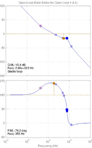
Using the values of Equation (2.10) in Equation (2.3) gives the transfer function for the open loop system, and a Bode plot of the transfer function is presented in Figure 2.5. From the Bode plot the symmetrical shape is confirmed and the phase margin = 87.8 degrees at the crossover frequency .U = 377 /O, see Figure 2.5.
The transfer function of the closed loop system can be calculated using Equation (2.4). A Bode plot on Figure 2.6 of closed loop system confirms the low pass filter behavior of the system.
Figure 2.5 Open loop frequency response.
Figure 2.6 Closed loop system frequency response.
2.3 Pulse Width Modulation(PWM)
The PWM modulators are open-loop voltage controllers, and the most common methods for PWM modulation is carrier based PWM, space vector modulation and random PWM. The main differences between these methods are described in [27]. Here only sinusoidal carrier based PWM technique will be described, since only this PWM is utilized in the project.
2.3.1 Sinusoidal PWM (SPWM)
The sinusoidal PWM techniques is easy for implementation and very popular for industrial converters. The PWM principle to control the output voltage is explained in Figure 2.7.
Figure 2.7 Principle of sinusoidal PWM for three phase VSI.
Figure 2.8 explains the general principle of SPWM, where isosceles triangle carrier wave is compared with fundamental frequency sinusoidal modulating wave, and the points of intersection determine the switching points of power devices. This method is also known as triangulation, subharmonic or suboscillation method. The notch and pulse widths of JQ wave vary in a sinusoidal manner so that the average of fundamental component frequency is the same as the frequency of
modulating signal and its amplitude is proportional to the command modulating voltage. The same carrier wave can be used for all three phases, as shown on Figure 2.7
Figure 2.8 Line and phase voltage waves of PWM voltage source inverter [27].
The maximum output voltage in the linear region when modulation index q is between 0 and 1 for SPWM is: ++= √2√23 = 0.612 r6 (2.11) and q = R ( (2.12)
2.4 Inverter Control Approaches
In a voltage source inverter (VSI) system the active power * and reactive power t can be controlled based on two distinct methods. The first approach is schematically illustrated in Figure 2.9 and is commonly referred to as voltage-mode control. The voltage-control mode has been mainly utilized in high voltage/power applications such as in Flexible Alternating Current Transmission System (FACTS) controllers, although industrial applications have also been reported. In this work, as an approximation we consider an infinite bus or a stiff voltage AC system. Thus, the AC system is modeled by an ideal three-phase voltage source. It is also assumed that grid voltages are sinusoidal and balanced (sometimes not really true in industrial and commercial installations) and of a relatively constant frequency. The VSI system of Figure 2.9 exchanges the real and reactive power components *u and tu with AC system, at the point of common coupling (PCC).
Figure 2.9 Schematic diagram of a grid-imposed frequency VSI system.
In voltage-controlled real/reactive power controller, the real and reactive power are controlled, respectively, by the phase angle and amplitude of the VSI AC-side terminal voltage relative to those of the PCC voltage. If the amplitude and phase angle of 456 are close to those of 456, the real and active power are almost decoupled and two independent compensators can be employed for their control. Thus the voltage-mode control has the merit of being simple and having a low number of control loops. However, since there is no control loop dedicated to the VSI line current, the VSI is not protected against overcurrents, and the current can undergo large excursions if the commands are changed rapidly or the AC system is subjected to a fault.
The second approach to control the real and reactive power in the VSI system of Figure 2.10 is referred to as current-mode control. In this approach, initially the VSI AC-side current is controlled by a dedicated control scheme, through the VSI terminal voltage. Then, both real and reactive power are
controlled by the phase angle and the amplitude of the VSI line current with respect to the PCC voltage. Thus, due to current regulation scheme, the VSI is protected against overload conditions. Other advantages of the current-mode control include the robustness against variations in parameters of the VSI and AC system, superior dynamic performance, and higher control precision [2].
Compared to the -frame, the -frame control of a grid-imposed frequency VSI system reduces the number of plants to be controlled from three to two. Moreover, instantaneous decoupled control of the real and reactive power, exchanged between the VSI system and the AC system, is possible in -frame. However, the control variables, that is, feedback signals, feed-forward signals, and control signals are sinusoidal functions of time. It is shown here that the -frame control of a grid-imposed VSI system features all merits of the -frame control, in addition to the advantage that the control variables are DC quantities in steady state. This feature remarkably facilitates the compensator design, especially in variable-frequency scenarios. Figure 2.10 shows a schematic diagram of a current-controlled real/reactive power controller, illustrating that the control is performed in frame. Thus, *! and t! are controlled by the line current components # and # . The feedback and feedforward signals (voltages and currents) are first transformed to the frame. Finally, the control signals are transformed to the frame and fed to the VSI (Figure 2.10). To protect the VSI, the reference commands # 8 and # 8 are limited by the corresponding saturation blocks (not shown in the Figure 2.10).
Figure 2.10 Schematic diagram of a current-controlled active/reactive power controller in frame.
In order to achieve zero-steady-state error in -frame control, the bandwidth of the closed-loop system must be adequately larger than the AC system frequency; alternatively, the compensators can include complex-conjugate pairs of poles at the AC system frequency and other frequencies of interest, to increase the loop gain. In - frame control, however zero steady state error is readily achieved by including integral terms in the compensators since the control variables are DC quantities. The -frame representation and control of a grid-imposed VSI system is also consistent with the approach used for the dynamic analysis of the large power system. The small-signal dynamics of the power system is conventionally modeled and analyzed in -frame.
2.4.1 Dynamic Model of Active/Reactive Power Controller
In a VSI system the active (*3 and reactive (t3 powers can be controlled based on two distinct methods. The first approach is schematically illustrated in Figure 2.9. In order to design the control system some simplifications can be done. For example, the filter term with the capacitor and damping resistor can be neglected. The dynamics of the full LCL circuit including the specification for a damped resonance will be discussed later.
Assume that the AC system voltage in the VSI system of Figure 2.9 is expressed as
4= sin ( ) 5 = sin ( −2;3 ) 6 = sin ( +2;3 )
(2.13)
where is the peak value of the line-to-neutral voltage, = . , . is the AC system (source) frequency. Dynamics of the AC side of voltage source inverter system on Figure 2.9 are described by the following differential equations:
(+y+ +X) # = − # + $− (2.14)
for our three phase system:
$4 = (+y+ +X) # J+ # J+ 4 $5 = (+y+ +X) # z+ # z+ 5
$6 = (+y+ +X3 # U+ # U+ 6 or in matrix form {## Jz # U | =1+ } $5$4 $6~ − + { # J # z # U | −1+ } 45 6~ (2.16)
For simplicity, it is considered that + = +y+ +X, = y+ X, where y and X resistances of first and second inductor respectively.
A common and often adopted approach in analyzing three-phase systems is to use a stationary or rotating frame [1]. In the first case the frame will be denoted as and in second as and it is also called synchronous. In fact the frame is synchronized with the angular speed . . The space vectors that express the inverter electrical quantities are projected on the axis and axis or on axis and axis.
The mathematical model in the frame is
• =
1
+ [ $ − − ]
=1+ [ $ − − ]
` (2.17)
It should be noted that the particular feature of the frame is that if a space vector with constant magnitude rotates at the same speed of the frame, it has constant and components while if it rotates at a different speed it has a time-variable magnitude (pulsating components). In the frame, differential equations for the current are dependent due to the cross-coupling terms . and . , and the equations also have feed forward terms and .
Thus a frame rotating at the angular speed . becomes
• = 1 + € $ − − • + . =1+ € $ − − • − . ` (2.18) or in matrix form
‚ $$ ƒ = ‚ ƒ + + ‚ ƒ „………†………‡ ˆ$&L ‰KJT$U! + +. ‚− ƒ „……†……‡ r UQŠI&$K + ‚„†‡ƒ 8 8Q "J L T (2.19)
2.4.2 Dynamic Model of Active/Reactive Power Controller
The power control of the grid inverter is based on the -frame power theory and as a consequence on the definition of the power in a reference frame, as discussed earlier. Typically the voltage oriented control is based on the use of a frame rotating at . speed and oriented such that the axis is aligned on the grid voltage vector. The space vector of the fundamental harmonic has constant components in the frame while the other harmonics space vectors have pulsating components. The main purpose of the grid inverter is to generate or to absorb sinusoidal currents; thus the currents reference components in the frame are DC quantities [2].
The reference current component #∗ is controlled to manage the active power control; while the reference current component #∗ controls the reactive power exchange and it is typically used to impress a desired power factor:
* =32 ( + ) (2.20)
t =32 ‹ − Œ (2.21)
Assuming that the axis is perfectly aligned with the grid voltage = 0, the active power and the reactive power will therefore be proportional to # and # respectively [2]:
* =32 (2.22)
t = −32 (2.23)
Figure 2.11 Control block diagram. 2.4.3 Current Regulator with a PI Control
The block diagram of the PI regulator is shown on Figure 2.12 and the transfer function is given by Equation (2.14)
Figure 2.12 Block diagram of PI controller.
The and control loops have the same dynamics (in ideal case of DC values), so the tuning of the PI controller for the current is done only for the axis. For the axis the parameters are assumed to be the same. As it can be seen from the current control block diagram in Figure 2.13, the voltage feed forward and the decoupling between the and axes has been neglected as they are considered as disturbances.
o PI controller with transfer function:
HR•(O3 = <I+<O$ (2.24)
o Control time delay block with transfer function:
HUQKL Q&(O3 =1 + O(1
! (2.25)
where (!=8y
Ž - sampling time for the control system
o Inverter block with transfer function:
H$K• L (O3 =1 + 0.5O(1
!" (2.26)
where (!"=8y
Ž• - switching period.
o Filter block is a simplified transfer function of the filter, that takes into account only the values of inductances and parasitic resistances:
H8$&L (O3 =+O +1 (2.27)
o Sampling block with transfer function:
H!JTI$K (O3 =1 + 0.5O(1
! (2.28)
The transfer function of the current loop can be calculated as:
HU& = HR•∗ HUQKL Q&∗ H$K• L ∗ H8$&L ∗ H!JTI&$K (2.29) The transfer function of the current loop can be written in a simplified manner as:
HU& =<IO + <O $1 + O(1 ‘y
<
(O( + 13 (2.30)
where < =y’, ( =’% and (‘y = (!+ 0.5(!"+ 0.5(!.
<IO + <$
O 1 + O(1 ‘y
<
O( + 1 =2O(‘y(1 + O(1 ‘y3 (2.31)
From Equations (2.32) and (2.33) <I and <$ can be identified and their values calculated, as:
<I=2<((
‘y = 11 (2.32)
<$ =<(I= 170 (2.33)
These values are used to start the analysis using Matlab toolbox, SISOtool. The Bode plot of the open-loop current control depicted in Figure 2.15. The step response is plotted in Figure 2.14. It can be seen that for continuous control system settling time of 0.00881s. is obtained.
2.4.4 Voltage Loop Control in Stand-Alone Mode
The previous section discussed the control and operation of a grid-imposed frequency VSI system in which the operating frequency can be predetermined and imposed by the AC system. In the absence of the utility grid, renewable energy systems could be used to provide energy to the local loads assuming and adequate supply of energy for the inverter to draw upon. The control structure on the DC and AC sides are changed to accommodate the needs of the local loads.
Figure 2.15 Open-loop Bode plot of the PI current control.
Unless there is battery backup in the system, the system cannot work on the principle of maximum power extraction from the source since this would lead to a sustained power imbalance. In stand-alone operation, the power transfer is dedicated primarily by the needs of the local loads. This section will translate the control of the grid-imposed frequency VSI system into the control of inverter output voltage and frequency, the system is shown on Figure 2.16.
Figure 2.16 VSI in stand alone mode.

![Figure 2.8 Line and phase voltage waves of PWM voltage source inverter [27].](https://thumb-eu.123doks.com/thumbv2/5dokorg/5520381.144002/34.918.176.737.227.929/figure-line-phase-voltage-waves-voltage-source-inverter.webp)