The opening effect, that means the reduction of conduc-tivity by stimulated electron-hole recombination is strongly dependent on the value of the direct recombination rate coef-ficient. Rate equation calculations with kd::::::
w--w
cm3 s-1,
characteristic for pure GaAs (Ref. 15) showed that with the same laser power and duration the conductivity drop is four orders of magnitude less than for kd
=
10-7 cm3 s-1•
Gen-erally, the faster the electron-hole pair recombination, the less laser energy is required to open the semiconductor switch.
In aU these calculations it was assumed that during the switching process transitions between impurity levels can be neglected. Second, it was assumed that nonlinear processes do not contribute to the population of energy l.eve1s. For high-power switches triggered by high-power lasers, multi-photon process impose limitations on the maximum obtaina-ble switch current density. Another limitation is given by impurity interactions and cluster formations at high-impuri<· ty concentrations.
The outstan.ding features of the described switch are that it can be turned on and turned otf on command without jitter on a nanosecond and faster timescale and that it does not require external energy to sustain the conductivity in the on state. The application of this type of switch is not limited to pulsed power systems, but can be extended to any system where bistable elements with fast temporal response and op--tical control are required.
This work was supported by Strategic Defense Initiative Organization/Innovative Science and Technology and
man-aged by the Office of Naval Research under Contract No. N000-14-86-K-560.
1K. H. Schoenbach, M. Kristiansen, and G. Schaefer, Proc.IEEE 71, 1019
(1984).
2G< Schaefer and K. H. Schoenbach, IEEE Trans. Plasma Sci. PS-14, 561
(1986).
3G. Mourou, W. H. Knox, and S. Williamson, PicG!Jecond Optoelectronic
Devices, edited by Chi H. Lee (Academic, Orlando, FL, 1984), p. 219.
4E. A. Chanchard, M. J. Phee, and Chi H. Lee, App!. Phys. Lett. 47, 1293
(1985).
5W. C. Nunnally, Proceedings of the 5th IEEE Pulsed Power Conference,
Arlington, VA, 1985, edited by M. F. Rose and P. J. Turchi (IEEE, New York, 1983), p. 235.
6J. D.
Morse, M.D. Pocha, IEEE Conference Record of the Seventeenth Power Modulator Symposium, Seattle, W A, 1986, edited by B. R. Gray (IEEE, New York, 1986), p. 211.
7
F. J. Zutavem, M. W. O'Malley, IEEE Conference Record of the Seven-teenth Power Modulator Symposium, Seattle, W A, 1986, edited by B. R. Gray (IEEE, New York, 1986), p. 214.
"L. Bovino, R. Youmans, M. Weiner, T. Burke, IEEE Conference Record of the Seventeenth Power Modulator Symposium, Seattle, WA, 1986, edit-ed by B. R. Gray (IEEE, New York, 1986), p. 219.
9I. Broser, R. Broser-Warminsky,
z.
Elektrochem. 61, 209 (19:57). 100. Madelung, Ed., Landolt-BOrnstein, Group Ill: Crystal and Solid StatePhysics, 17b (Springer, New York, 1982), p. 417.
11R. Germer, S. Pronko, and K. H. Schoenbach (unpublished).
12J. Blanc, R. H. Bube, and H. E. McDonald, J. Appl. Phys. 32, 1666
(1961 ).
13N. Kullendorf, L. Jansson, and L. A. Ledebo, J. Appl. Phys. 54, 3203
(1983).
14
D. V. Lang and R. A. Logan, J. Electron. Mater. 4, 1053 (1975).
15M. S. Demokan and M. S. Ozyazici, Int. J. Electron. 55, 699 ( 1983}.
Anisotropic plasma .. chemical etching by an electron ... beam .. generated
plasma
T. R. Verheya> and
J. J.
RoccaNSF ERC for Optoelectronic Computing Systems and Department of Electrical Engineering, Colorado State University, Fort Collins, Colorado 80523
P. K. Boyer
Tektronix Solid State Research Laboratory, Tektronix, Inc., Beaverton, Oregon 97077 (Received 6 August 1987; accepted for publication 17 November 1987)
Anisotropic etching of Si02 has been achieved with a plasma generated by a broad-area low-energy ( 150-300 eV) electron beam in a He+ CF4 atmosphere. Etch rates of up to 330 A/min for Si02 and 220 A/min for Si were obtained. Etching occurred with good uniformity over the entire area exposed to the electron-beam-generated plasma. The fluxes of energetic charged particles to the sample surface are discussed in relation to their possible contribution to the etching process.
We report the first experimental demonstration of an-isotropic etching of Si02 achieved with the assistance of an electron-beam-generated plasma. It has been previously shown that enhancement of Si02 , Si3 N4 , and Si etching is
obtained through the use of energetic electrons. •-3 In com-parison with ion beams of the same energy, beam electrons induce less crystalline damage.1 Consequently, low-energy electron-beam-assisted etching has been proposed as source of low-damage etching.
•> M.S. student in the Physics Dept. Coburn and Winters demonstrated that Si3 N4 and Si02
are readily etched in a XeF2 atmosphere when assisted by a 1500-V, 50 mA/cm2 small-area electron beam2
• The non~ thermal increase in the rate of plasma-chemical etching ofSi and Si02 in a CF4
+
02 atmosphere under bombardmentby 200-e V electrons was reported by Kireev et aU These experiments have demonstrated an increase in etch rate in the presence of an electron beam, but did not describe the etched profiles.
Here we report the anisotropic etching of Si02 in a
He+ CF4 plasma created by a low-energy (150-300 eV) broad-area electron bea..'TI. Single-crystal ( 100) Si has also been etched in the same environment. In our experiment, a 1.9-cm-diam electron beam was used to decompose CF4
molecules into reactive radicals and provide a directed flux of energetic electrons to the sample surface.
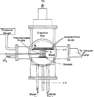
A schematic diagram of the experimental setup is shown in Fig. 1. A novel hollow cathode discharge electron gun was developed to produce a well·-collimated beam of electrons in a He
+
CF4 atmosphere at pressures up to 0.1 Torr. In thisenvironment, our electron source can produce de electron beams with current densities up to 15 mA/cm2
at energies between 100 and 1000 eV. Details of the design, operation, and characterization of the broad-area low-energy electron source are discussed in another publication.4 The electron source and a water-cooled sample support platform are en-closed in a cross-shaped stainless-steel vacuum vessel with
10-cm-diam ports. The samples to be etched were placed on the platform so that the beam strikes at normal incidence. The platform was maintained at the same potential as the outer grid of the electron source to form a nearly field-free negative glow region between the sample and the electron gun. The distance between the electron gun and the sample was adjustable, and tests at 0. 7, 1.4, and 2.2 em were per-formed, The chamber was evacuated to 10-3 Torr with a
Water. In
He
Acceleration Grids
FIG, L Schematic diagram of the experimental setup. The thermocouple probe was used to monitor beam power density. A second thermocoupie (not shown) was soldered with indium to a Si sample to measure wafer temperature.
2464 J, Appl. Phys., Vol. 63, No.7, 1 Apri11988
rotary pump, and a rotameter~controlled flow of gases was established. Helium was flowed through the hollow cathode of the electron source to make the operation of the discharge relatively independent of the reactive gas in the etching re--gion. CF4 was flowed into the reaction chamber at a rate of
490 seem, which is large enough to ensure that the etch rate is not limited by an insufficient amount of reactant gas.
Both Si02 and Si were readily etched in a 50-mT He+ 30-mT CF4 environment under a variety of electron
beam conditions. Si02 films, 1.5 pm thick, were thermally
grown over a ( 100) Si substrate. The Si substrates were 15-20-fl-cm boron-doped ( 100) silicon wafers. For the etch profile studies, masking was done with AZ-5214 resist that was deep UV (A.
=
254 nm) stabilized and hard baked for 60 min at 150 cc to insure mask integrity during eteching.Figure 2 shows a linear dependence of the etched step height in Si02 and Si as a function of etching time. The
constant slopes give etching rates of 175 and 85 A/min, re-spectively. The samples were etched at 2.2 em from the gun with an electron beam current density of3.0 mA/cm2 and an acceleration voltage of 175 V.
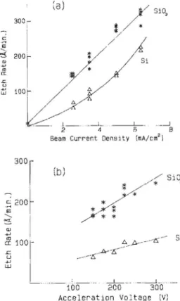
The etch rate dependencies of Si02 and Si as a function of electron beam current denstiy and energy were studied. Substrate heating imposes a limitation on the maximum val-ues of the electron beam current density and energy. Exces-sive heating causes photoresist reticulation and degradation and thermal etching. The electron beam current was moni-tored during the etching by measuring the current collected by the acceleration grid. The beam current density at the sample position was previously measured with a calorimeter and correlated to the acceleration grid currents.
Figure 3(a) shows the increase of the etch rates ofSi02 and Si as a function of electron beam current density. The data were taken for an electron beam acceleration voltage of 175 eV. While the etch rate of Si02 was found to increase
linearly with electron beam current density in the entire range investigated, the etch rate of silicon increased at a larg-er rate at high ( > 3 mA/cm2
) beam current densities. A
linear increase in the etch rate might be expected since the rate of production of reactive radicals by electron impact collisions increases linearly with current density. Also, an increase in the dissociation rate of adsorbed radicals and
6000r ~ ~ .c "' ;;; 4000 I "'-"' _,_, <f) ~ 2000 .c .::; lLJ -.-. ______1...___-- _ _______j__ ___ - - _ ______j_-_ j 10 20 30 40 Etch Time(min.)
FIG. 2. Variation of the etched step height as a function of time forSi02 and
Si. The atmosphere was 50-mT He+ 30-mT CF., the electron beam cur-rent density at the sample position was 3.0 rnA/em\ the acceleration vol-tage was 17 5 V, and the sample was positioned 2, 2 em from the gun.
Verhey, Rocca, and Boyer 2464
Downloaded 06 Jul 2006 to 129.82.233.53. Redistribution subject to AlP license or copyright, see http://jap.aip.orgfjap/copyright.jsp
(a)
Y
Si02300,-~
/*
~
I / /i
r.,
r
/ /"
~
taa1/
c./
>
K
~-- - . 1 -····-- L .... _ L _. __ _ j 2 4 0 8Beam Currer.t Density (mA/cm2)
(b)
- s i
: - --- _ J _ _ ___ __ _ _ L. ... --100 2CO 300
Acceleration Voltage (V)
FIG. 3. (a) Etch rate ofSiO, and Si as a function of electron beam current density at the sample. The bea:n energy was 175 V. (b) Etch rate of Si02
and Si as a function of eiectron beam energy. The beam current density at the sample position was 3.0 rnA/em', the atmosphere was 50-rnT He+
30-mT CF4 , and the distance between the gun and sample was 2.2 em. The
small SiO, etch rate in the absence of the electron beam was a consequence of 30 min of exposure of the sample to plasma diffusing from the electron gun without beam acceleration voltage applied.
electron-stimulated desorption of etching products5
-6 should result from an increased electron beam flux. The ad-ditional increase in the Si etch rate is probably due to the thermal component of the etching. Measurements of the wa-fer temperature under the corresponding beam conditions
show an increase in wafer temperature from 60
·c
at 2.5mA/cm2 to 148
oc
at 6.4 mA/cm2•
Figure 3(b) illustrates the etch rate dependence as a function of the electron beam energy in the range between 1 SO and 300 e V, for a constant electron beam current density
of 3.0 mA/cm2 incident on the sample. Both the Si0
2 and Si
etch rates increase with beam energy in this range, but the Si rate increase is less pronounced. Collisional production of the etching radicals in the electron-beam-generated plasma
decreases slightly over the energy range investigated.7
Sub-sequently, the etch rate would be expected to decrease. The
observed increase might be due in part to secondary
elec-trons emitted from the sample surface, 1 which can
contrib-ute to the creation of reactive radicals.
The anisotropic profile of an etched Si02 feature 1.0 f.LID
wide is shown in Fig. 4. No resist undercut was observed in the Si profiles, however the sidewalls were significantly sloped.
In previous electron-beam-assisted etching experi-ments, the observed enhancement of the etching rates was
2465 J. Appl. Phys., Vol. 63, No.7, 1 April1988
FIG. 4. Etched profile in Si02 • The feature was etched at i 50 V for 90 min in
He+ CF4 atmosphere at a distance of 0.7 em from the gun. The upper
layer, designated by th~ line, is AZ-5214 photoresist. Below the line is a SiO, film on a Si substrate.
attributed to beam electrons.2·3 Nevertheless, the
contribu-tion of energetic ions possibly existing in the electron beam plasma used here and in some of the experiments reported in
the literature3 cannot be ignored. There are two mechanisms
which couid potentially contribute to the anisotropic etch-ing observed in the experiments reported here: direct surface impingement by beam electrons and bombardment by
nega-tive ions created by electron attachment and dissociation in
the source and accelerated through the potential difference between the grids of the electron gun. The bombardment of
the surface by positive ions accelerated across the plasma
sheath formed between the bulk of the electron-beam-gener ..
ated plasma and the sa.mple is unlikely to play a significant
role. The voltage drop across the plasma sheath was
calcu-lated from a simple model of the sheath to be less than 1.0 eV.
This is a consequence of both the low energy ( ""'0.1 eV) of
the thcrmalized secondary electrons created by ionization in
the beam generated plasma8 and the secondary electrons
emitted from the substrate surface. In this energy range, the
secondary electron emission (SEE) coefficients of Si02 , Si,
and resist polymer are greater than one.9 Emitted secondary
electrons serve to neutralize the substrate surface and lower
the sheath potential.9 Further measurements, including that
of the electron temperature in the He+ CF4
electron-beam-generated ph1.sma, are still required to verify our
assump-tions and to determine with certainty the role of energetic
positive ions in the etching process.
The contribution of negative ions cannot be easily ne··
glected since the reactant gas can diffuse upstream into the
electron source and result in their formation. While CF4
practically does not capture thermal electrons, Jo,u the
de-composition products of the molecule could result in a
sig-nificant concentration of negative ion species, mainly
p- .12
-14 In order to estimate the possible energetic negative
ion flux, we introduced an electrostatic probe into the elec-tron source plasma above the acceleration grids. From the Langmuir probe trace, it is possible to obtain rough
measure-ments of the negative ion density to electron density ratio.13
The ion saturation current portion of the probe trace enabled
us to calculate the positive ion density, an.d the density of negative ions was obtained from the condition of quasineu-trality of the plasma. This technique does not allow an accu-rate measurement of the ion density to be made. However, it can be used to set an upper limit for the presence of a negative ion current. Measurements made at typical electron source operating conditions gave an electron density of 1 X 10¹⁰
em·~· 3 and indicated that the negative ion density could be of
the same order. Considering the F-- to electron mass ratio, the maximum energetic ion flux is estimated to be 1% of the electron beam current density and could consequently amount to ion beam current densities of up to 60 f.1A/cm2
•
Even if the negative ion flux is expected to be approximately 100 times smaller than the measured electron beam flux, it cannot be completely neglected since, from previous experi-ments in XeF2 , the yield of ions was measured to be an order of magnitude larger than that of beam electrons. 1 Further
studies are required to determine the relative role of negative ions in assisting anisotropic etching in electron-beam--gener-ated plasmas.
In summary, we have demonstrated anisotropic etching of Si02 in a He+ CF4 electron~beam-generated plasma, Etching was observed to occur over the entire surface ex-posed to the electron beam with good uniformity and can be scaled to larger areas with dt"-etron guns currently available. 4
The possible contribution of energetic ions in electron-beam-assisted etching experiments cannot be neglected and should be more carefully studied.
The authors want to thank R. Chow, T. Douglas, T. Ash, A. Chou, K. Bremmer, and J. Rose for their assistance and to acknowledge an earlier collaboration with G. Collins and Z. Yu. This work was supported by National Science Foundation (NSF) Grant No. CPE-84.08304, the NSF ERC for Optoelectronic Computing Systems (Grant No. CDR-8622236), and the Colorado Advanced Technology Institute. J. J. Rocca is an NSF Presidential Young Investi-gator.
'R. R. Kunz and T. M. Mayer, J. Vac. Sci. Techno!. B 5, 427 (1987).
2
J. W. Coburn and H. F. Winters, J. Appl. Phys. 50, 3189 ( 1979).
3V. Yu. Kireev, M.A. Kremerov, V. L. Kustov, and S.D. Pekarchuk, Sov.
Tech. Phys. Lett. 7,467 (1981).
"T. R. Verhey, J. J. Rocca, and P. K. Boyer,J.Appl. Phys. 62,3001 (1987). 'T. E. Madey and J. T. Yates, Jr., J. Vac. Sci. Techno!. 8, 525 ( 1971 ).
'M. A. Loudiana and J. T. Dickinson, J. Vac. Sci. Techno!. B 3, 1393 (1985).
7
H. F. Winters and M. Inokuti, Phys. Rev. A 25, 1420 ( 1982).
•z.
Yu, J. J. Rocca, G. Collins, and C. She, Phys. Lett. 96A, 125 ( 1983).9H. R. Kaufma:1 and R. S. Robinson, Operation of Broad-Beam Sources
(Commonweal Scientific, Alexandria, VA, 1987), Chap. 16, p. 234.
10
R. W. Fessenden and K. M. Bansal, J. Chem. Phys. 53, 3468 ( 1970).
11
R. Schumacher, H.-R. Sprunken, A. A. Christodoulides, and R. N. Schindler, J. Phys. Chem. 82,2248 ( !978).
'2S. Klagge, M. Maas, and A. Serov, Beitr. Plasmaphys. 25,255 ( 1985).
"J. Meichsner, H. U. Poll, and K. N. Wickleder, Contrib. Plasma Phys. 25, 503 {1985).
14D. Edelson and D. L l<lamm, J. Appl. Phys. 56, 1522 ( 1984).
Dielectric measurements on substrate materials at microwave frequencies
using a cavity perturbation technique
D. C. Dube,a> M. T. Lanagan, J. H. Kim, and S.
J.
JangMaterials Research Laboratory, The Pennsylvania State University, University Park, Pennsylvania 16802 (Received 15 October 1987; accepted for publication 2 December 1987)
A cavity perturbation resonance technique suitable for microwave measurements on substrate materials is discussed. The technique makes use of thin rectangular samples placed in a rectangular waveguide cavity (
Q
~ 5000). The availability of advanced microwavemeasurement equipment makes it possible to record experimental data at several frequencies (five in this present case). The estimated accuracy of measurements is
± 2% for dielectric
constant and 3 X 10···4 for dielectric loss. Results are reported in the 8.2-12.4-GHz frequency range for alumina and specially prepared silica.Higher computer speeds and increasing use of microwaves in advanced navigation and domestic ap-pliances require that electrical properties of materials be known at high frequencies. Substrates in microwave inte-grated circuits and packaging system assemblies have dielec-tric constants in the range from 2 to 10 and dielecdielec-tric losses
(tan 8) lower than 10-3
. Therefore, a measurement tech-nique which can measure dielectric parameters with high precision and accepts thin specimens is highly desirable.
ods at microwave frequencies, a widely used one is that de-veloped by Roberts and von Hippel. 1 The technique loses
accuracy for thin sheet specimens encountered in substrate and packaging materials. 2 Chao3 has discussed other sources of error occurring in short-circuit line methods in general. Alternative techniques have been worked out for thin speci-mens.4--S
Cavity perturbation methods have been widely used in the measurement of dielectric parameters of materials. The perturbation theory of resonant cavities was first proposed by Bethe and Schwinger.9 The assumptions were further re-defined by Spencer, LeCraw, and Aultw and Waldron.11 Among the reflection-transmission measurement
meth-•J On leave from Indian Institute of Technology, New Delhi 110016, India.