MASTER THESIS
Effect of Growth Time, Growth
Temperature and Light on Growth
Mechanism of C60 nanorods
Master`s Thesis within the Master`s program in Physics
ABASI ABUDULIMU
SUPERVISOR
HAMID REZA BARZEGAR GOLTAPEHEI
EXAMINER
THOMAS WÅGBERG
Department of Physics
Umeå University
Umeå, Sweden 2013
I
Abstract
In this thesis work C60 nanorods were produced by Liquid-Liquid Interfacial
Precipitation method (LLIP) assisted with 10 s of weak sonication. Ethanol and m-dichlorobenzene were used as poor and good solvents of C60, respectively. Five different
temperatures, 4, 10, 20, 30, 40 and 50 , were chosen as growth temperatures of different samples to investigate the effect of temperature on the grown structures. Different samples were prepared in the dark and under the light with various growth time to determine the effect of light and growth time on growth of C60 nanorods. The
characterization of the grown C60 nanorods were conducted by transmission electron
microscopy (TEM) and x-ray diffraction (XRD). The result of characterization indicated that the sonication introduced smaller C60 nanostructures; light irradiation and
temperature increase (till 40 C0) during the growth time resulted in nanorods with smaller diameter, whereas the long growth time lead to the increase of the diameter of C60
nanorods. The as-grown C60 nanorods synthesized at different conditions possess an hcp
II
Contents
Chapter 1. Introduction and theory ………... 01
1.1 C60 ………... 02
1.2 Fullerene One Dimensional Structures ………... 03
1.3 LLIP Method ………... 05
1.4 Characterization Methods ……….... 07
1.4.1 Transmission Electron Microscopy ………... 07
1.4.2 X-Ray Diffraction ……….. 09
Chapter 2. Experiment ………. 13
2.1 Synthesis of C60 Nanorods ………. 14
2.2 Sample Preparation for XRD ………... 16
2.3 Sample Preparation for TEM ………... 17
Chapter 3. Result and Discussion ………. 19
3.1 The Grown Sample ……… 20
3.2 Result from TEM Measurement ……… 21
3.2.1 Temperature effect on growth mechanism of C60 nanorods ………... 23
III
3.2.3 Light effect on growth mechanism of C60 nanorods ……….. 27
3.3 Result from XRD ………... 30
Conclusion ………... 32
Acknowledgment ………... 34
- 1 -
Chapter 1
- 2 -
1.1 C
60C60 was discovered by Harold Kroto et al. at Rice University in 1985 [1], and Kroto,
Curl and Smalley got Noble Prize for that in 1996. C60 is a hollow spherical molecule
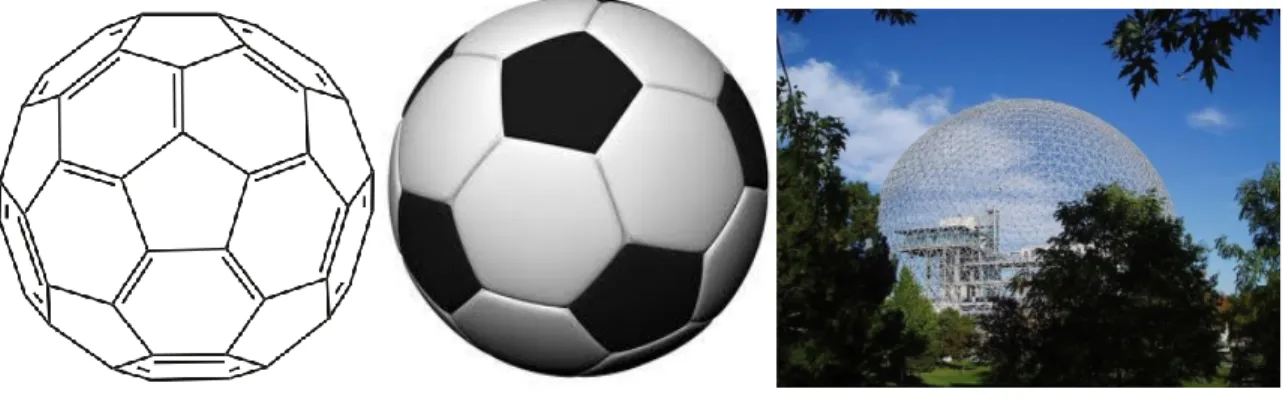
containing 60 carbon atoms, which is also used to call Buckminsterfullerene after an architect R. Buckminster Fuller who pioneered the use of geodesic domes in architecture. It is also commonly referred to Bucky balls due to their football like shape. The similarity of C60 structure to football and geodesic domes are shown in Figure 1.
Figure 1. Similarity of C60 (left) with football (middle) and geodesic dome (right)
One C60 molecule contains 20 hexagons and 12 pentagons, one carbon atom at each
corner; they are arranged such that there is no common side for two pentagons. The size of the C60 molecule is about 1.034 nm in diameter [2] and the bond length in average is
0.14nm (carbon-carbon double bonds are shorter than the single bonds). [3] In contrast to diamond and graphite, where every carbon atom forms primary bonds with other neighbor atoms throughout the whole solid [4], the carbon atoms in C60 bond together and
- 3 -
interacting with other material, and it is also possible to entrapping atoms and small molecules at the interior of the C60 molecule without any reaction.[5]
The discovery of C60, followed by a great effort on investigation of its structure,
properties and applications in semiconductor, superconductor, medicine and composite materials.[6-7] It is found that, in the solid state, the sixty carbon atoms form a crystalline structure and pack together in a face-centered cubic array. It is as soft as graphite but becomes super hard when compressed to certain percent of its volume.[8-9] C60 is
electrically insulating material as a pure crystalline solid [10], but easily reacts with electron reach molecules because of its electron deficient alkene like behavior; and can be semi-conductive [11], whose conductivity increases with increasing temperature, metallic
[12]
or superconductive [13-14] with proper impurity addition.
1.2 Fullerene one dimensional structures
C60 one dimensional structure was first observed by Miyazawa et al. in 2001, when
they were preparing lead zirconate titanate (PZT) thin films by using C60 contained PZT
sol (see Figure 2(a)).[15-16] In general fullerene one dimensional structures are constructed from a series of fullerene molecules (like C60 or C70) by the help of van der Waals force [17]
and depending on the morphology they are called fullerene rods or tubes. It is also common to use the terms fullerene nanorods, nanowhiskers or nanotubes when the fullerene structure has diameter less than 1000 nm and length of several micrometers. The developed techniques to fabricate fullerene one dimensional structures, so far, included
- 4 -
(LLIP) [18-19], template method [20], solution evaporation method [21], rapid synthesis method [22], surface-assistant method [23] and vapor-solid process.[24] Among those, the LLIP method has been the most attractive one due to its simplicity, applicability at room temperature and no need to catalysts or templates. [24-25]
Figure 2. (a) SEM image of C60 nanorods in a PZT sol containing C60 [16]
, (b) TEM image of the first C60 nanorods synthesized by LLIP.
[35]
The typical fullerene nanorods prepared by LLIP method have diameter of less than 500 nm and length of greater than 100 um, while for tubes the diameter reaches to a few micrometer and length to centimeter.[26,27,28] The rods are normally single-crystals, while the tubes, depending on the growth method and condition, have mono-crystalline, polycrystalline or amorphous structure. [17] Due to the bulk availability of C60 [29] and its
potential application in optoelectronic devices [30-31], optical switching applications [32],
- 5 -
solar cells [33] and field effect transistor [34] the synthesis of nanorods/tubs from fullerene molecules has become quite interesting topic, and many interesting techniques has been developed.
1.3 LLIP Method
After the discovery of C60 nanowhiskers, in 2002 Miyazawa et al. developed a new
method to fabricate crystalline fullerene nanorods/tubes by slowly adding isopropyl alcohol to a C60 saturated toluene solution. This is known as liquid-liquid interface
precipitation method (LLIP).[35] Figure 2(b) shows the TEM image of the first C60
nonanrods synthesized by LLIP method.
In general in the LLIP method, a poor solvent of fullerene (e.g. alcohols) is gently added onto a solution of C60 in a good solvent (e.g. m-xylene) in such a way that a clear
interface forms between two solvents. Due to diffusion of good and poor solvents a fullerene saturated mixed state forms at the interface which causes the nucleation of fullerene crystals (crystal seeds) at the interface. By further diffusion of two solvents the fullerene one dimensional crystal structures; rods or tubes (depending on the experimental condition) grow on the crystal seeds. [18] The later method is so called Static LLIP method. [36] One could also increase the diffusion rate by the help of sonication or hand shaking. [37] Figure 3 shows optical and SEM images of the C60 nanorods and tubes
- 6 - Figure 3. Optical micrograph (a, c) and SEM image (b, d) of C60 nanorods and tubes produced by
LLIP.[28]
Although a great progress has been made by the LLIP method, the growth mechanism is not clear yet. [25] Nevertheless, it has been well known that the temperature, light, water content of the poor solvent and the solvent ratio have significant impact on the growth mechanism of fullerene nanorods/tubes. [6, 38-39] In this work we study the effect of temperature, light and growth time on the growth of C60 nanorods synthesized by LLIP
method.
(c) (d)
(b) (a)
- 7 -
1.4 Characterization Methods
Characterization is the key to understand any kind of material and its systematic development. Understanding the crystal structure, morphology and the chemical composition of fullerene nanostructure is believed to be the most important way to explore its growth mechanism, which most likely leads to the possibility of controlling the dimension and morphology of the grown fullerene nanorods/tubes. In this project we used optical microscope, X-ray diffraction (XRD), Transmission electron microscope (TEM), as the most frequently used techniques [40], to characterize the crystal structure of the synthesized C60 nanorods. A brief description about TEM and XRD is given in the
following two subsections.
1.4.1 Transmission Electron Microscopy
TEM is a type of electron microscopy which utilizes a beam of high energy electrons and electromagnetic lenses instead of a beam of light and normal optical lenses. In general the short wavelength of the electrons and their interaction with the material provide information about morphology, crystal structure and chemical composition of nanostructures. A typical TEM consists of an electron sources (a thermionic or field emission gun), condenser lenses, sample holder, objective lenses, projector lens, phosphor or fluorescent screen and different apertures. [41] Figure 4 shows the structure of a typical TEM and the schematic explanation of its operation principles.
- 8 - Figure 4. Typical TEM (left) and a schematic view of its operation principles (right). [40]
The electrons, provided by the electron gun, would be accelerated by the applied voltage to the condenser lenses. Then the condenser lenses guide the electron beam to the sample on the sample holder. The electrons then interact with the sample and directed to the florescent screen through objective and projector lenses. Finally, the CCD camera [42] provides the picture of the specimen. In order to increase the mean free path of the electrons and avoid any interaction of the electrons with the impurities, different parts of
- 9 -
the TEM are placed in a vacuum chamber. It is also important to have thin enough specimen to let the electron beam pass through that.[43]
The image can be manipulated by adjusting the accelerating voltage to increase or decrease the speed of electrons (which in turn change the electromagnetic wavelength of the electrons) as well as adjusting the electromagnetic lenses.[44] The De Broglie equation (equation 1) connects the wave length of electron to its energy so that faster (or more energetic) electron leads to the shorter wavelength for electrons and consequently gives higher resolution and better image quality.[45]
(1)
Where and p are wave length and momentum of electron respectively and h is Planck`s constant.
1.4.2 X-Ray Diffraction (XRD)
X-ray is a form of electromagnetic radiation with relatively short wave length and high energy, and would be absorbed or scattered when it is interacting with a matter. It is called hard X-ray when the photon energies are above 5 keV, otherwise called soft x-ray. Since the wavelength of the hard X-ray is comparable to the size of the atom their interaction with the materials can be used to gain information about the crystal structure of the materials.[46] XRD is one of the most popular analytical methods to study crystal
- 10 -
structure and chemical composition of materials; and the Bragg`s diffraction model gives a better explanation for it, see the Figure 5.
Figure 5. Diffraction of X-rays from the planes in a crystal
In Bragg`s model, a crystal is thought of a set of parallel planes, specified by the so called Miller indices (h, k, l), which intersects the atoms of the unit cell. When a beam of X-ray impinges on parallel atomic planes with angle it would be scattered by the atoms in different directions and will be combined constructively or destructively. Strong intensities appears (known as Bragg peaks) when the condition for constructive interference satisfies the Bragg`s equation.[47] In other words, the constructive interference appears when the path length differences of the two incident beams 1 and 2 in Figure 5 equals to an integer number of the wavelength:
- 11 -
(3)
Equation (3) is known as Bragg`s law, where is an integer, λ is the wavelength of incident ray, is the perpendicular distance between two closest parallel lattice planes,
called d-spacing. The magnitude of the d-spacing could also be expressed as a function of Miller indices (h, k, l) and lattice parameters (a, b, c). The expression becomes more complicated for less symmetrical crystal systems. Equation (4) shows the simplest form simple cubic crystal system:
√ (4)
In a XRD measurement, a beam of X-ray from an X-ray tube strikes on a continuously rotating sample (see Figure 6(a)) and a recorder automatically plots the intensity of the diffracted beam versus the diffraction angles 2by moving on the goniometer. Figure 6(b) shows one of the XRD patterns of C60 nanorods recorded by our setup. The obtained
data then could be analyzed by combining the Bragg`s equation with the equation of d-spacing. Overall, since the wave length of the X-ray is fixed, by measuring the X-ray incident angle 2at corresponding intensity peaks one could easily obtain the value of the d-spacing ( ) by Bragg`s equation and the lattice parameters could also be found by equation (4) once the Miller indices are known. It would be much easier if the crystal system is known and the system has higher symmetry such as cubic crystal system.[48-49] Normally this procedure could be done by the help of some software like “Panalytical Xpert High Score” with huge database.
- 12 - Figure 6. (a) XRD set up, (b) shows a XRD pattern of the C60 nanorods.
[28]
(a)
- 13 -
Chapter 2
- 14 -
2.1 Synthesis of C
60Nanorods
The C60 nanorods were produced by LLIP method as explained in theoretical part.
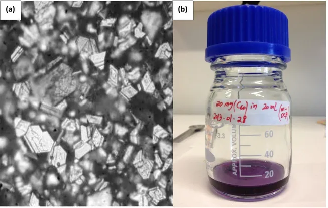
Ethanol (99.5%; from Kemetyl) and m-dichlorobenzene (99.0%; from Sigma-Aldrich) were used as poor and good solvents of C60 respectively. The black crystalline C60
powder, Figure 7(a), with purity of 99.9% (from MER Corporation) was degassed in a vacuum chamber for 12 hours at 150 to remove any possible gases. After degassing, the C60 powder was dissolve in m-dichlorobenzene with a concentration of 1.0 mg/ml
(Figure 7(b)). The prepared solution was sonicated in an ultra-sonic bath (USC300D-VWR) for 45 minutes and thereafter stored in room temperature for 24 hours to get a stable solution.
Figure 7. C60 powder (a) and prepared C60/m-DCBM solution (b)
- 15 -
The samples were prepared as follow: 10 ml ethanol was gently added to 1.0 ml of prepared C60/m-DCBM solution (in 15 ml vial) to form a clear interface between two
solvents as shown in Figure 8. Thereafter the sample was kept at desired temperature for four days, which we call growth time. During the growth time the lower pinkish phase start to disappear and the grown structures precipitated at the bottom of the bottle.
Figure 8. Prepared sample out of C60/m-DCB solution and ethanol (a) and similar sample after
weak sonication which result in formation of third yellowish phase (b).
Five different temperatures, 4, 10, 20, 30, 40 and 50 , were chosen as growth temperatures for different samples to investigate the effect of temperature on the grown structures. For each set of experiment two samples were prepared, one was directly stored
- 16 -
in an incubator at desired temperature, Figure 8(a), while the other one, Figure 8(b), was stored in incubator after 10 s of weak sonication (the power setting is two on an USC300D from VWR). The sonication was applied to increase the nucleation rate at the interface which probably results in smaller crystal seed and consequently growth of C60
nanorods with smaller diameter.
2.2 Sample Preparation for TEM
Figure 9. Sample preparation for TEM: (1) C60/m-DCBM + ethanol solution which contains
- 17 -
A transmission electron microscope (JEOL 1230), with acceleration voltage of 80 kV, was employed to observe the grown C60 nanostructures. The sample for TEM
measurement was prepared as follow (see Figure 9): the dispersion containing grown C60
nanorods was strongly hand shaken for few minutes. Then TEM grid, with holey carbon film, was immersed into the dispersion. To make sure that the larger structures are on the grid, in some cases TEM grid was drop casted by the dispersion (containing nanorods/tubes). The measurements were carried out on the dried grid.
2.3 Sample Preparation for XRD
The samples for X-ray diffraction (XRD) measurement were prepared by filtering the dispersion containing the grown C60 nanorods with a 0.45 um Polytetrafluoroethylene
(PTFE) filter as shown in figure 10(a). The C60 nanorods were annealed at 50 for 15
minutes on a hot plate to evaporate the remaining solvents. Thereafter the filtered structures were deposited onto the XRD sample holder; see Figure 10(b). Each XRD measurement was executed immediately after sample preparation using Siemens D5000 diffractometer with an accelerating voltage of 40 kV and wavelength (Cu Kα) of 1.5418 Å.
- 18 - Figure 10. Sample preparation for XRD: (A) filtering setup, (b) the filtered structures are mounted onto the XRD sample holder after annealing
- 19 -
Chapter 3
- 20 -
3.1 The Grown Sample
As mentioned in the experimental part, the C60 nanorods start to grow at the nucleation
sites at the interface of ethanol and C60/m-DCB solution and the grown structures deposit
at the bottom of the bottle. Figure 11 shows the hand shaken samples four days after preparation.
Figure 11. Grown samples with four days of growth time: a) non-sonicated, b) sonicated
Samples stored directly after preparation, without any interruption to the interface of two liquids contained very thick and long C60 nanorods or tubes. As shown in Figure
11(a) it is possible to see the large needle like crystal structure by naked eyes which are
- 21 -
dispersed in a fully colorless solution. However the grown structures are not homogenous with respect to diameter and length which indicates that at the early stage of the growth (nucleation) the crystal seeds were not homogenous in size. In contrast the samples stored after a weak sonication (Figure 11(b)) contained yellowish structures which were confirmed to be C60 nanorods by TEM measurements.
Since samples without sonication contained C60 structures with randomly size
distribution we did not consider those samples for statistical analysis, instead the main focus in this work is on the samples assisted with sonication, with homogenous size distribution, to study the effect of the growth time, growth temperature and light effects on the grown C60 structures.
3.2 Result from TEM Measurement
Figure 12(a) shows a TEM image of the grown C60 nanorods four days after
preparation, the results revealed that samples assisted with weak sonication mainly contained C60 nanorods. According to the earlier work of our group, large crystal seeds
promote the growth of tubular C60 structure in contrast to the small crystal seeds which
mainly result in the growth of C60 nanorods.[28] The weak sonication applied to the
liquid-liquid interface creates numerous small and homogenous nucleation sites which consequently results in the growth of small diameter C60 nanorods. However TEM
measurements on the similar sample four hours after preparation indicated that some of the nanorods have tubular shape close to the tips, as shown in figures 12(c) and 12(d).
- 22 - Figure 12. C60 nanorods (a) and tubes (c) grown for 4 days and 4 hours respectively. The
magnified image showing the tip of a nanorod (b) and tube (d)
According to the growth model of C60 one dimensional nanostructure, proposed by
Heng. X. J et al., [22] the C60 molecules prefer to settle down at the edges of the crystal
seed, since the edges are energetically more favorable compare to the center (edges have
(a) (b)
- 23 -
lower free energy). Therefore within the first few hours of the growth it is possible to see tubular form at the tips of the nanorods which will be filled later for longer growth time. As expected, we did not find any tubes in the samples grown longer than one day. It could be recognized from Figure 12 that each grown C60 nanorods and tubes have uniform
diameter along its entire length. Another feature of the grown C60 nanorods and tubes is
that the tips of the nanorods are pointed, while it is flat in tubes.
3.2.1 The effect of growth time on the growth of C60 nanorods
We have noticed that the diameter of the C60 nanorods grown under the light increased
after few weeks, e.g. the diameter of C60 nanorods grown under the light increased from
220 nm (at 4 days of growth time) to 250 nm after 30 days. To make sure if this result comes from the effect of light or the long growth time we prepared few more samples in various growth time in the dark and under the light. The result, Figure 13 and Figure14, revealed that the diameter of the C60 nanorods increased gradually with increasing the
growth time not only under the light but also in the dark. It is known that the nanorods start to grow on crystal seeds in two directions at the same time, during growth time if there are enough C60 molecules available, the diameter of the C60 nanorods may increase
by formation of new C60 layers on their surface, [28] therefore longer growth time may
increase the diameter of the nanorods. The change is significant at the beginning of the growth (when there are more free C60 molecules) process. We have also checked the
diameter of the grown C60 nanorods after three months of storing in original bottle, and
- 24 - 4 24 48 72 0 50 100 150 200 250 300 D iameter (n m)
Growth time (hours)
Figure13. Average diameter of the as-grown C60 nanorods (under the light) at different growth
- 25 - 24 48 72 0 50 100 150 200 250 300 D ia m e te r (n m )
Growth time (hours)
Figure14. Average diameter of as-grown C60 nanorods (in dark) at different growth time, the error
bars show standard error of mean.
Based on these results we could say that the growth time is another important parameter to be considered to control the dimensions of the fullerene nanorods. By comparing Figure 13 and Figure 14, one could notes that the diameter of the grown C60
nanorods under the light is slightly larger than the one in the dark, and the question about light effect comes up. This effect will be explain further later
- 26 -
3.2.2 Temperature effect on the growth of C60 nanorods
4 10 20 30 40 50 0 50 100 150 200 250 300 350 400 M ean D iameter (n m) Temperature (C0)
Figure15. Average diameter of the as-grown C60 nanorods (with sonication) at different growth
temperature, the error bars show standard error of mean for each set of data.
The average diameters of the grown C60 nanorods, synthesized at different temperature,
are calculated by measuring the diameter of more than hundred nanorods of each sample. All the samples are tested four days after preparation. Figure 15 illustrates that the average diameter of the grown C60 nanorods decreased with increasing the growth
temperature below 40 Cº, thereafter the diameter increased by increasing the growth temperature.
- 27 -
This result indicates that temperature is another important parameter which affects the final structure of the grown C60 nanorods. The result can be explained by using the
growth time effect described in previous section. In fact at low temperature the solubility of C60 in m-DCB and ethanol decreases and C60 saturation close to the interface of two
solvent occurs at shorter time on the other word growth rate is higher at low temperature, therefor shorter time will be needed to form certain thickness of nanorods. While in higher temperature the solubility of C60 is higher which decreases the saturation rate and
growth rate, thus longer growth time is needed to form thicker nanorods. Therefore same growth time results in the growth of thicker nanorods at low temperature compare to one grow at higher temperature. On the other hand further increase of temperature above 30 Cº probably results in fast diffusion of two solvents into each other and again the saturation rate and consequently the growth rate increases which again results in the growth of thicker nanorods within same growth time.
3.2.3 Light effect on the growth of C60 nanorods
To see the effect of the light on the growth of C60 nanorods, we prepared few more
samples again in the dark and under the light, both at room temperature. The result of TEM measurement, presented in Figure 16, indicates that the C60 nanorods grown under
the light have smaller diameter than the one in the dark. To make sure if this result is reliable we repeated this experiment, and the result turned out to be the same.
- 28 - 0 50 100 150 200 250 Light M ean D iameter (n m) Dark
Figure16. Diameter comparison of C60 nanorods grown in the dark and under the light at room
temperature, the error bars show SE error of mean.
The result of light effect on the diameter of C60 nanorods could be somehow, supported
by the work of M. Tachibana et al [50]. According to their report the growth rate of C60
nanorods promoted significantly even by weak light irradiation, and estimated that the phenomena could mainly be from the interaction between the electric field of light and solute molecule. However, the diameter of the grown C60 nanorods in their experiment
- 29 -
The reason for the result of diameter change under the room light irradiation in our experiment could be due to the small differences in growth temperature between the samples synthesized in dark and under the light. We think that the growth temperature was slightly lower for sample synthesized in dark compare to the one synthesized under the light and lead to thinner rods. Another reason could be that under the light illumination the growth is much faster along the length of the C60 nanorods in such a way
that the free C60 molecules prefer to seat at the tip of the nanorods than the surface of the
nanorods. More experiments are needed for clear explanation of this result.
- 30 -
3.2 X-Ray Diffraction Measurement Result
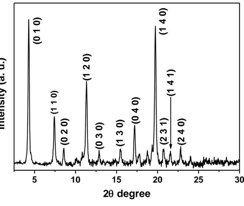
5 10 15 20 25 30 (2 4 0) (1 4 1) (2 3 1) (1 4 0) (0 4 0) (1 3 0) (0 3 0) (1 2 0) (0 2 0) (0 1 0)
Intens
ity (
a. u.)
2 degree (1 1 0)Figure17. XRD pattern of the as-grown C60 nanorods grown in the dark at room temperature
The crystal structures of obtained C60 nanorods under various growth conditions such
as different growth temperatures, different growth time, with and without light irradiation were examined by powder XRD. The result revealed that regardless of the growth condition all synthesized nanorods have hexagonal close-packed (hcp) crystal structure. However intensity of the peaks for different reflection changed between the samples which might be due to different orientation of the nanorods on the XRD sample holder. Figure 17 shows a typical XRD pattern of the as-grown C60 nanorods (grown in dark and
- 31 -
at room temperature). An assignment of the peaks specifies an hcp crystal structure with unit cell size of a=b= 23.861 Å and c= 10.144 Å. This result is similar to the previous works suggesting same crystal structures for C60 structures grown out of a solution of C60
in m-DCB or toluene (see Figure 6). [73] We believe that the hcp crystal structure of the as-grown nanorods will change into face-centered cubic (fcc) crystal structure upon annealing at appropriate temperature (due to evaporation of solvent molecules) in inert ambient, as already proved by previous reports. [38, 44, 48] The crystal lattices reconstruction through the displacement of C60 molecules could be the reason for the
structure transformation from hcp to fcc when the annealing is applied to the as-grown C60 nanorods.[43] Overall different growth condition did not make any change on the
- 32 -
Conclusion
Samples prepared by LLIP method without sonication contain very thick and long C60
rods, in contrast the samples assisted with weak sonication contain long C60 nanorods
with smaller diameter The nucleation sites are believed to be the key to determine the diameter of the C60 nanorods, due to the small nucleation sites at the liquid-liquid
interface, introduced by a weak sonication, the grown C60 nanorods appeared to be much
smaller in diameter compare to the non-sonicated one. Mainly C60 nanorods were
obtained in all samples assisted by weak sonication. The reason for that could be the absence of large crystal seeds (nucleation sites) at the interface of two solutions. Since the only large nucleation sites are account for the tubular structure.
The average diameter of the grown C60 nanorods decreased as the growth temperature
increased from 4 to 30 C°. By further increase of temperature, above 30 C0, the diameter of the nanorods increased again, however diameter increase at high temperature became less significant. This effect could be explained by higher saturation rate of C60 at lower
temperature. Fast diffusion of two solvent at high temperature also increase the C60
saturation rate, since the solubility of C60 in mixture of m-DCB and ethanol decrease significantly
By synthesizing samples with various growth times we found that the diameter of the C60 nanorods increases with increasing growth time, this increase is significant at the
- 33 -
beginning of the growth process, and it happens for both samples grown in the dark and under the light.
The light illumination of the samples during the growth period results in the growth of C60 nanorods with smaller diameter compare tothe one in the dark. It is well known that
the growth rate of fullerene nanorods/tubes could be promoted significantly by light irradiation.
- 34 -
Acknowledgment
I am very grateful to Prof. Thomas Wågberg for giving me the opportunity to work on this nice project as well as all his support and help during my research work in his group. I would like to thank my supervisor Hamid for his outstanding supervise, nice advice, great support during the whole project and precious comments on my report which gave me a big help to improve my work quality. Florian, Tiva and Guangzhi deserve special mention as their friendliness introduced me a really comfortable environment to work with.
- 35 -
References
1. Kroto H. W; Heath J. R; O'Brien S. C; Curl R. F; Smalley R. E. Nature. 318, 6042, 162–163, (1985).
2. Morton R. “Nano-Surface Chemistry”. Marcel Dekker Inc. Pp. 98-100. (2002).
3. Hedberg K; Hedberg L; Bethune D; Brown C; Dorn H; Johnson R. Science. 254, 5030, 410-412, (1991).
4. Steven S; Susan A. “Chemistry”, 5th ed. Houghton Mifflin Press. Pp. 470-476. (2000).
5. Buckminsterfullerene: http://www.azom.com/article.aspx?ArticleID=3499. 6. Hotta K, Miyazawa K. J. Phys. Conf. Ser. 159, 012021, (2009).
7. Andreas H; Michael B. “Fullerenes: Chemistry and Reactions”. Wiley – VCH Press. Pp. 1-33. (2005).
8. http://arxiv.org/abs/0704.2504.
9. http://toxnet.nlm.nih.gov/cgi-bin/sis/search/a?dbs+hsdb:@term+@DOCNO+7714.
10. William D. C; David G. R. “Material Science and Engineering”. SI Version Eighth Edtion, John Wiley & Sons Pte Ltd. Pp. 468-471. (2011).
11. Katz E. A; Soga T. “Nanostructured materials for solar energy conversion”.
Elsevier. Pp. 361–443. (2006).
12. Gunnarsson O. Reviews of Modern Physics. 69, 2, 575, (1997).
13. Hebard A. F; Rosseinsky M. J; Haddon R. C; Murphy D. W; Glarum S. H; Palstra T. M; Ramirez A. P; Kortan A. R. Nature. 350, 6319, 600, (1991).
- 36 -
14. Ganin A. Y; Takabayashi Y; Khimyak Y. Z; Margadonna S; Tamai A; Rosseinsky M. J; Prassides K. Nature 7, 5, 367–71, (2008).
15. Miyazawa K.; Yano J.; Kaga M.; Ito Y.; Maeda R. Surf. Eng. 16, 239, (2000). 16. Miyazawa K.; Obayashi A.; Kuwabara M. J. Am. Ceram. Soc. 84, 3037, (2001). 17. Miyazawa K. “Fullerene Nano-Whiskers”. Pan Stanford Publishing Pte. Ltd. Pp.
1-18. (2012).
18. Miyazawa K.; Kuwasaki Y.; Hamamoto K.; Nagata S.; Obayashi A.; Kuwabara M.
Surf. Interface Anal. 35, 1, 117–120, (2003).
19. Liu H. B.; Li Y. L.; Jiang L.; Luo H. Y.; Xiao S. Q. J Am. Chem. Soc. 124, 13370–1, (2002).
20. Wang L.; Liu B. B.; Yu S. D.; Yao M. G.; Liu D. D.; Hou Y. Y.; Cui T.; Zou G. T.; Sundqvist B.; You H. Chem. Mat. 18, 4190–4194, (2006).
21. Jin Y.; Curry R. J.; Sloan J.; Hatton R. A.; Chong L.; Blanchard N. J. Mater. Chem.
16, 3715–20, (2006).
22. Ji H. X.; Hu J. S.; Tang Q. X. J. Phys. Chem. C. 111, 28, 10498–10502, (2007). 23. Shin, H. S.; Yoon, S. M.; Tang, Q.; Chon, B.; Joo, T.; Choi, H. G. Angew. Chem., Int.
47, 693, (2008).
24. Yongtao Q.; Wenwen Y.; Nana N.; Shaocen L.; Guibao L.; Guangzhe P. Cond. Matt.
Phys. 10, 5402. (2012).
25. Miyazawa K.; Hotta K. J. Cryst. Growth. 312, 2764–2770, (2010).
26. Zhang Y.; Liu W.; Jiang L.; Fan L.; Wang C.; Hu W.; Zhong H.; Li Y.; Yang S. J.
- 37 -
27. Miyazawa K.; Minato J.; Mashino T.; Yoshii T.; Kizuka T.; Kato R.; Tachibana M.; Suga T. M. P. Conf. Seattle, SMS-23, (2005).
28. Hamid R. B.; Florian N.; Artur M.; Leszek S.; Cheuk W. T.; Thomas W. Molecules.
17, 6840-6853, (2012).
29. Guibao L.; Ping L.; Zhu H.; Guangzhe P.; Jian Z.; Shao X. L.; Guangye L. Mater
Lett. 64, 483-485, (2010).
30. Xia Y. N.; Yang P. D.; Sun Y. G.; Wu. Y. Y.; Mayers B.; Gates B. Adv. Mater. 15, 353, 89. (2003).
31. Zhang X. Z.; Jiao K.; Piao G.; Liu S. F.; Li S. X. Synth Met. 159, 4, 19–23, (2009). 32. Xing Y. J.; Jing G. Y.; Xu J.; Yu D. P.; Liu H. B.; Li Y. L. Appl. Phys. Lett. 87, 26,
(2005).
33. Somani P.; Somani S.; Umeno M. Appl. Phys. Lett. 91, 17350, 3–5, (2007).
34. Ogawa K.; Nobuyuki A.; Miyazawa K.; Nakamura S.; Mashino T.; Bird JP.; Ochiai Y. J Appl. Phys. 47, 501–504, (2008).
35. Miyazawa K.; Kuwasaki Y.; Obayashi A.; Kuwabara M. J. Mater. Res. 17, 1, 83–88, (2002).
36. Miyazawa, K.; Hotta, K. J. Nano. Part. Res. 13, 5739–5747, (2011).
37. Miyazawa K.; Minato J.; Yoshii T.; Fujino M.; Suga T. J. Mater. Res. 20, 688, (2005).
38. Hotta K.; Miyazawa K. Nano. 3, 355–359, (2008).
- 38 -
40. Yizheng J.; Richard J. C.; Jeremy S.; Ross A. H.; Lok C. C.; Nicholas B.; Vlad S.; Harold W. K. J. Mater. Chem. 16, 3715–3720, (2006).
41. Gabor L. H.; Joydeep D.; Harry F. T.; Anil K. R. “Introduction to Nanoscience”. CRC
Press. Pp. 136. (2008).
42. Williams, D.; Carter, C. B. “Transmission Electron Microscopy”. Plenum Press. Pp. 18-34. (1996).
43. Cowley, J. M. “Diffraction physics”. Elsevier Science B. V. North Holland Press. Pp. 176-192. (1995).
44. Rose, H. H.; Sci. Technol. Ad. Mater. 9, 014107, (2008).
45. Champness, P. E. “Electron Diffraction in the Transmission Electron Microscope”.
Garland Science. Pp. 28. (2001).
46. David A. “Soft X-rays and extreme ultraviolet radiation”. Cambridge University
Press. Pp. 2, (1999).
47. Rohrer. G. S. “Structure and Bonding in Crystalline Materials”. Cambridge University
Press. Pp. 205-206, (2005).
48. William D. C; David G. R. “Material Science and Engineering”, SI Version Eighth Ed. John Wiley & Sons Pte Ltd. Pp. 69-108. (2011).
49. Cahn R. W.; Haasen P.; KRAMER E. J. “Material Science and Technology”.
WILEY-VCH. Pp. 277-279. (2005).
50. Tachibana M.; Kobayashi K.; Uchida T.; Kojima K.; Tanimura M.; Miyazawa K.
- 39 -
51. Watanabe K.; Miyazawa K.; Kojima K.; Tachibana M. IEEJ Trans. SM 128, 321, (2008).
52. Minato J.; Miyazawa K. Diam. Relat. Mater. 15, 1151, (2006). 53. Minato J.; Miyazawa K. Carbon. 43, 2837-2841, (2005).
54. Sathish M.; Miyazawa K.; Sasaki T.; Diam. Relat. Mater. 17, 571, (2008). 55. Sathish M.; Miyazawa K. Nano. 3, 409, (2008).