M¨
alardalen University
School of innovation, design and engineering
Master thesis in Electronics
Evaluation of partial reconfiguration in
FPGA-based high-performance video
systems
Author: Emil Segerblad emil.segerblad@gmail.com Supervisor: Dr. Mikael Ekstr¨om Examiner: Prof. Lars AsplundAbstract
The use of reconfigurable logic within the field of computing has increased during the last decades. The ability to change hardware during the design process enables developers to lower the time to market and to reuse designs in several different products. Many different archi-tectures for reconfigurable logic exists today with one of the most commonly used are Field-Programmable Gate Arrays (FPGA). The use of so called dynamic reconfiguration, or partial reconfiguration, in FPGAs have recently been introduced by several leading vendors but the concept has existed for several decades. Partial reconfiguration is a technique were a specific part of the FPGA can be reprogrammed during run-time. In this report an evaluation of partial reconfiguration is presented with focus on the Xilinx ZynQ System-On-Chip and the GIMME2 vision platform developed at M¨alardalen University. Special focus has been given to the use of partial reconfiguration in high-performance video systems such as the GIMME2 platform. The results show that current state of the technology is capable of performing reconfigurations within strict timing constraints but that the associated software tools are yet lacking in both performance and usability.
Sammanfattning
Anv¨andningen av rekonfigurerbar logik inom ber¨akningsomr˚adet har ¨okat under de senaste de-cennierna. M¨ojligheten att ¨andra h˚ardvaran under designprocessen kan hj¨alpa utvecklare att s¨anka utvecklingstiderna och att ˚ateranv¨anda konstruktioner i flera olika produkter. M˚anga olika arkitekturer f¨or rekonfigurerbar logik existerar idag och en av de vanligaste ¨ar Field-Programmable Gate Arrays (FPGA). Anv¨andningen av s˚a kallad dynamisk omkonfigurering eller partiell omkonfigurering i FPGA: er har nyligen inf¨orts av flera ledande leverant¨orer men konceptet har funnits i flera decennier. Partiell omkonfigurering anv¨ands f¨or att ¨andra en specifik del i h˚ardvaran under k¨orning. I denna rapport presenteras en utv¨ardering av partiell omkon-figurering p˚a FPGA:er med fokus p˚a Xilinxs ZynQ System-On-Chip och GIMME2-plattformen som utvecklats vid M¨alardalens h¨ogskola. S¨arskilt fokus har lagts vid anv¨andningen av par-tiell omkonfigurering i h¨ogpresterande videosystem s˚asom GIMME2-plattformen. Resultaten visar att den nuvarande tekniken ¨ar kapabel att utf¨ora partiella omkonfigureringar inom strikta tidsbegr¨ansningar men att de tillh¨orande verktygen (mjukvaran) ¨annu har klara brister i b˚ade prestanda och anv¨andarv¨anlighet.
Acknowledgements
The path of the righteous man is beset on all sides by the iniquities of the selfish and the tyranny of evil men. Blessed is he who, in the name of charity and good will, shepherds the weak through the valley of darkness, for he is truly his brother’s keeper and the finder of lost children. And I will strike down upon thee with great vengeance and furious anger those who would attempt to poison and destroy My brothers. And you will know My name is the Lord when I lay My vengeance upon thee.
- Jules Winnfield, ”Pulp Fiction”, 1994 I chose this quote not because I am a religious person, on the contrary, I chose it because it sounds cool and also due to the fact that it is something that you would not expect a hitman to say just before killing a man. It makes you think, does it not? Now, before I get all philosophical, there are some people I would like to thank for making this master thesis possible. First of all I would like to thank Sara, my fianc´ee, for her great support during these past 4 years. Furthermore, I would to thank my family and friends for their interest and support of my work. I would also like to thank my room mates at MDH: Fredrik, Carl, Ralf and Batu for not throwing me out when I was annoying and also for their good ideas and feedback. Lastly, I would like to thank my supervisor Mikael Ekstr¨om at MDH for good support and ”can-do”-attitude and my examinator Lars Asplund at MDH for good feedback and challenging tasks.
Glossary
API Application Programming Interface 46, 48
ARM Advanced Reduced Instruction Set Computer (RISC) Machine 17 ASIC Application Specified Integrated Circuit 1, 10
AXI Advanced eXtensible Interface 17, 31–33, 36, 37, 41, 46 BIOS Basic Input/Output System 39
BLE Basic Logic Element 10 CAN Controller Area Network 41 CCD Charged Coupled Device 7
CPLD Complex Programmable Logic Device 9, 10 CPU Central Processor Unit 3, 10, 13, 50
DDR Dual Data Rate 36, 41, 46, 47, 58 DMA Direct Memory Access vi, 18, 35, 46 DSP Digital Signal Processor 14
EDK Embedded Development Kit 33, 34 EMIO Extended Multiplexed I/O 18
EPP Extensible Processing Platform iv, 3, 17, 19
FPGA Field Programmable Gate Array 1–3, 5, 6, 10–17, 22–25, 27, 28, 31–33, 39, 40, 48–53 FPS Frames Per Second 27, 28, 46
FSBL First-Stage Boot-Loader 40
GIMME General Image Multiview Manipulation Engine 5 GPIO General Purpose Input/Output 41
GPS Global Positioning System 7 GPU Graphics Processing Unit 23
HDL Hardware Description Language 1, 3, 5, 11, 52 HLS High-Level Synthesis 1, 2, 6, 37, 51, 53
I/O Input/Output 33
IC Integrated Circuit 10, 13, 16
ICAP Internal Configuration Access Port v, 15, 25–28, 33–36, 46, 49, 50, 52 IEEE Institute of Electrical and Electronics Engineers 31
IP Intellectual Property 6, 15, 16, 39, 48, 50, 58
ISE Integrated Software Environment 14–16, 34, 36, 38, 45, 51 LIDAR LIght Detection and Ranging 7
LUT Look-Up Table 10, 14
MDH M¨alardalen University 41, 51, 53 MIG Memory Interface Generator 41 MIO Multiplexed Input/Output 40
MIPS Microprocessor without Interlocked Pipeline Stages 8
PCAP Parallel Configuration Access Port 16, 17, 31–34, 36, 45, 46, 49–52 PCI Peripheral Component Interconnect 14, 23
PL Programmable Logic 1, 9, 10, 17, 18, 31, 35, 39–41, 45, 46, 49, 50 PS Processing System 17, 18, 31–33, 35, 36, 40, 41, 46, 49, 50
RAM Random Access Memory 14
RISC Reduced Instruction Set Computer ii, 17 RTL Register Transfer Level 1
SD Secure Digital 40, 48
SDK Software Development Kit 40
SoC System on Chip 5, 17, 18, 31, 39, 40, 49 SRAM Static Random Access Memory 27 USB Universal Serial Bus 39
VDMA Video Direct Memory Access 36, 37, 47, 50
VHDL VHSIC Hardware Description Language v, 37, 47, 50 WSN Wireless Sensor Networks 27
List of Figures
1.1 Figure showing a comparison between various hardware architectures. Picture is
from the work of Flynn and Luk. [25] . . . 2
1.2 Figure showing the concept behind dynamic reconfiguration. . . 3
1.3 Figure showing a wrongly performed partial reconfiguration. . . 4
2.1 Figure showing the concept of an stereo-camera setup taken from the work of Ohmura et al. [55] . . . 8
2.2 Video flow example. . . 8
2.3 Filtering example fromhttp://rsbweb.nih.gov/ij/plugins/sigma-filter.html 9 2.4 Feture extraction example fromhttp://www2.cvl.isy.liu.se/Research/Robot/ WITAS/operations.html . . . 9
2.5 MIPS pipeline . . . 10
2.6 Figure showing the mobile robot used by Weiss and Biber (left) and the output 3D map (right). The image is from the work of Weiss et al. [64] . . . 10
2.7 Figure showing the general concept of an FPGA-device. The figure is from the article by Kuon et al. [48] . . . 11
2.8 Figure showing a typical Look-Up Table (LUT). [49] . . . 11
2.9 Picture from lecture slides from NTU. [8] . . . 12
2.10 Figure showing how a LUT can be ”programmed” to perform logic operations. [49] 12 2.11 Figure showing the general concept of an FPGA-device. The figure is from the article by Kuon et al. [48] . . . 13
2.12 Figure showing a typical island style partition location strategy. . . 15
2.13 Figure showing the outline of the Xilinx RP. [35] . . . 16
2.14 The layout of the DevC-module. [38] . . . 18
2.15 Figure showing the general idea on how to utilize the Xilinx Extensible Processing Platform (EPP)-family. [41] . . . 19
2.16 Figure showing the outline of the Xilinx ZynQ-SoC. Image from Xilinx document UG585. [38] . . . 19
2.17 Figure showing the ZC702 board peripherals. [41] . . . 20
2.18 Figure showing the outline of the GIMME2 platform. [3] . . . 20
2.19 Figure showing the GIMME2 boards front (right) and backside (left). Notice the two image sensors on the backside of the PCB (encircled in red). Also notice the Zynq SoC (encircled in yellow, the PS DDR Memory (encircled in blue) and the PS DDR Memory (encircled in purple). . . 21
3.1 Figure showing the system from the article by Hosseini and Hu. [29] To left is the logic implementation and to the right is the CPU implementation using the Altera Nios II. . . 23
3.2 System developed by Ohmura and Takauji. Picture is retrieved from the article by Ohmura and Takauji. [55] . . . 23
3.3 System developed by Ohmura and Takauji. Picture is retrieved from the article by Ohmura and Takauji. [55] . . . 24
3.4 Komuro et al.’s architecture. [47] . . . 24
3.5 Blair et al.’s performance. [14] . . . 25
3.6 Figure showing Ming et al.’s results taken from their article. [51] . . . 27 3.7 Koch et al.’s implemented system. Picture is taken from the related article. [45] . 28
3.8 Ackermann et al.’s system. [2] . . . 29
4.1 Figure showing the Partial Reconfiguration flow from WP374. [23] . . . 33
4.2 Excluded partial reconfiguration steps from XAPP1159 shown in red. [46] . . . . 34
4.3 Reference design with Microblaze and Internal Configuration Access Port (ICAP) added. . . 35
4.4 Reference design from XAPP1159. . . 36
4.5 Implemented video design. . . 37
4.6 Second implemented video design. . . 38
4.7 Red filter code. . . 39
4.8 Color filter code. . . 42
4.9 Work flow for Partial Reconfiguration in Xilinx ISE from UG702. [35] . . . 43
4.10 Example boot image format for Linux. Picture from UG821. [37] . . . 43
4.11 Example boot image format for Linux. Picture from UG873. [36] . . . 44
5.1 Excerpt from VHSIC Hardware Description Language (VHDL)-code generated by Vivado HLS. . . 47
7.1 Proposed video pipe line. . . 51
A.1 Macro definitions. . . 58
A.2 Memory access code. . . 58
List of Tables
3.1 Figure showing the results from work by Hosseini and Hu. [29] The first four rows are for the filtering of a 64 x 64 pixel image while the last two are for the filtering
a 256 x 256 pixel image. . . 22
3.2 Komuro et al.’s performance. [47] . . . 25
3.3 Meyer et al.’s results. [53] . . . 26
3.4 Table showing Ming et al.’s results taken from their article. [51] . . . 26
3.5 Ackermann et al.’s results. [2] . . . 28
3.6 Ackermann et al.’s results. [2] . . . 29
3.7 Bhandari et al.’s results. [11] . . . 30
3.8 Perschke et al.’s results. Picture from the related article. [58] . . . 30
3.9 Perschke et al.’s results. Picture from the related article. [58] . . . 30
5.1 Figure showing the time needed to just finish the ”write”-function call on the ZC702 board running Linux. . . 45
5.2 Figure showing the time needed for the full reconfiguration flow on the ZC702 board running Linux. . . 45
5.3 Figure showing reconfiguration time needed to finish the Direct Memory Access (DMA)-transfer on the ZC702 board using standalone software. . . 46
Contents
List of Figures iv
List of Tables vi
Introduction 1
Thesis description . . . 4
Scope of this report . . . 5
Outline of this report . . . 6
Background 7 Introduction to computer vision and its applications . . . 7
Introduction to Programmable Logic (PL) . . . 9
Field Programmable Gate Array-technology . . . 10
Run-time Reconfigurability with focus Xilinx FPGA . . . 12
Heterogeneous systems . . . 16
Computer Vision on FPGAs and heterogeneous systems . . . 17
Xilinx ZynQ-7000 and Xilinx XC702 . . . 17
GIMME 2 . . . 18
Related work 22 Implementations of computer Vision on FPGAs . . . 22
Implementations of reconfigurable FPGA-systems . . . 24
Implementations of reconfigurable FPGA-systems running computer vision algorithms 27 Method 31 Early work . . . 31
Design considerations . . . 31
Method of reconfiguration . . . 34
Implemented vision components . . . 36
System design in Xilinx ISE/Planahead . . . 38
Interface from Linux . . . 39
GIMME2 . . . 39
Results 45 Performance of reconfiguration methods . . . 45
Vision component implementation . . . 47
Software implementation evaluation . . . 48
GIMME2 . . . 48
Discussion 49
Future work 51
Bibliography 54 Appendix A Device interface from Linux 58 Appendix B Overview of Xilinx ZynQ-family 59
Introduction
Within the world of computation one of the largest open questions is which hardware platform, or architecture, to use for a certain task. Some platforms can achieve high clock frequencies but low degrees of parallelism while others can achieve high degree of parallelism but are limited to lower clock frequencies. Each architecture has its own inherent strengths and weaknesses. Designers are often faced with the problem of choosing the right platform for the right task, which is not always an simple problem to solve as costs, availability and design support also play a major role during development and production. Hence, performance is not always the most important aspect to consider when choosing a platform.
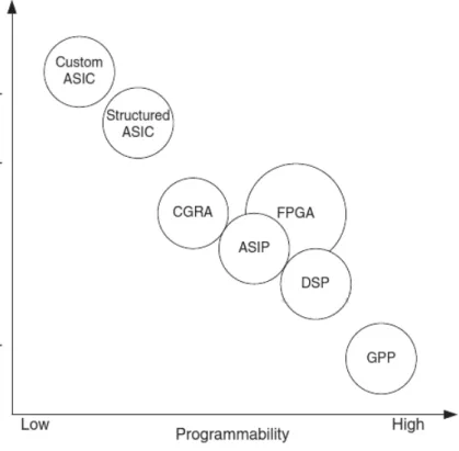
Today many applications exist where both performance and costs are critical aspects. The industry standard for many years to use for such applications have been to design and imple-ment Application Specified Integrated Circuits (ASICs). ASICs have the advantage of being cheap to produce and allows for high performance in general. ASICs are not without problems, however. Long development times, expensive in small to medium-scale production and no re-programmability after production are some its inherent disadvantages. Other technologies such as Field Programmable Gate Arrays (FPGAs) allows designer to shorten the design phase and allows for a high-degree of re-programmability after production. FPGAs belongs to a much larger family known as Programmable Logic (PL) where focus is on the programmability of the hardware and can jokingly be refereed to as ”Lego-logic” due to its high degree of custom-ability. The use of PL has increased over the years in embedded systems due the good flexibility and decent performance that the various PL-architectures offer. However, the reconfigurable nature of PL-devices also has some drawbacks, such as much lower speed (in terms of clock frequency) than other processing architectures. What the PL-architectures lack in speed they gain in parallelism. The ability to run tasks in parallel on PL borders to the extreme. An comparison between various hardware architectures with respect to performance and programmability can be found in figure 1.1.
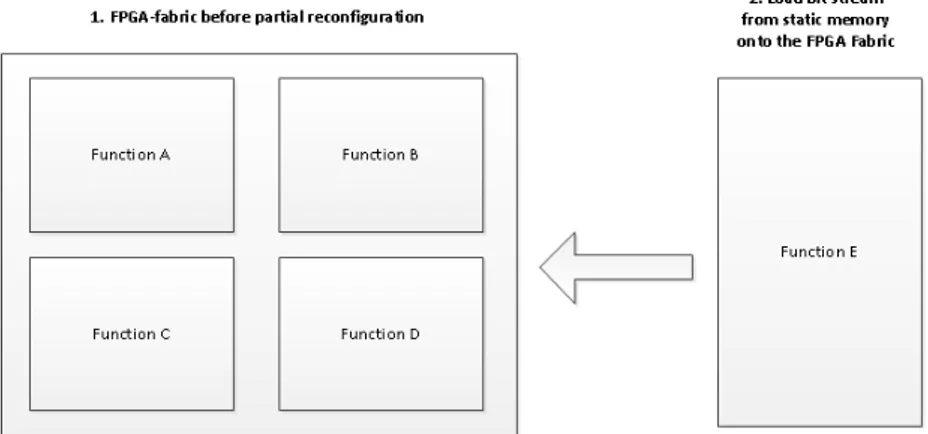
Some PL-systems are reconfigurable during run-time. That means that one or several sec-tions of the logic fabric can be reprogrammed with or without affecting the operation of other sections depending on which technique is used. Run-time reconfiguration enables developers to dynamically use hardware-acceleration in their applications by changing the behaviour of the logic. Furthermore, by swapping functions in and out of the FPGA chip area can be saved. An example of this concept, known as partial reconfiguration, can be seen in figure 1.2. At first the FPGA-fabric contains functions A-D. At some point the user wants to put function E on to the FPGA and hence functions B and D, in this example, must be overwritten in order to make function E fit properly.
Some important aspects seen in figure 1.2 needs further explanation. All bit streams (a stream of data containing the new configuration of the PL) for the functions to be used in the system needs to be generated prior to run-time and stored in non-volatile memory in order to minimize reconfiguration delay and ensure a deterministic system behaviour (generating bit streams during run-time is currently impossible as the time needed is vast). In most cases the tasks put on the FPGA are generated manually by the developer using Hardware Description Language (HDL) but lately tools for automatic HDL-code generation from high level languages have appeared on the market. One example of such a tool is Xilinx Vivado High-Level Synthesis (HLS). Vivado HLS is able to generate Register Transfer Level (RTL)-level code from high level languages, such as: C/C++ and Matlab. RTL, not to be confused with Resistor-Transistor
Figure 1.1: Figure showing a comparison between various hardware architectures. Picture is from the work of Flynn and Luk. [25]
Logic, is a common abstraction mechanism used in hardware design where synchronous circuits are modelled as the data flow between registers and the manipulation performed on the data flow. For more information about Xilinx Vivado HLS, please refer to the Vivado HLS User guide. [33].
When doing partial reconfiguration there exists a risk for corruption of previously existing functions. An example can be seen in figure 1.3.
As can be clearly seen in figure 1.3, if a component is placed badly on to the FPGA it can destroy or interfere with other pre-existing components. Therefore, it is of uttermost importance that the user keeps tracks of the boundaries of all components on the FPGA in some manner. This is however, tiresome and error prone to do ”by hand” so a better option to ensure compo-nent integrity is to implement a resource manager that keeps track on where the functions are placed and during partial reconfiguration makes sure that no pre-existing component is affected negatively. This task is highly complex and not without problems. A third option also exists and that is to divide the area of the chip in to different regions with different properties. Most common is to have one region being static, that is non-reconfigurable, and then several regions that can be reconfigured. Using high-level design tools, the user can then verify that non of the tasks to be put into one of these regions violates any design rules or other limitations. After this is verified the functionality of each region can be changed dynamically during run-time with-out any concern that the reconfiguration would affect any other region. However there exists some limitations on partial reconfiguration, both software-wise and hardware-wise, as will be presented later in this report. Furthermore, some different ways of partitioning the FPGA-logic between static and reconfigurable areas will be briefly explained in the Background-section.
The applications of this technology are many. The ability to put software tasks on hardware are appealing, especially for systems with a strong degree of possible parallelism in them. An example here would be computer vision systems, where large chunks of data needs to be processed in real-time. Vision systems also have a high degree of parallelism making them ideal for hardware acceleration. However, the software used in modern vision systems are often complex and written in high-level languages such as C++ or Java. Porting such complex tasks to an
Figure 1.2: Figure showing the concept behind dynamic reconfiguration.
FPGA would be extremely hard as many of the constructs used in high-level languages have no direct representations in HDL. However, some tools exist, such as Vivado HLS that was presented earlier in this text, for High-level language to HDL-conversion. These tools are not without limitations though, as will be seen later in this report.
Instead of creating new specialized functions for each implementation, a library of vision algorithms and tools are often used in software design. One popular library for computer vision is OpenCV. OpenCV contains several high-level functions for image processing such as Hough transforms, color conversion algorithms and feature extraction methods. The OpenCV-library is compatible with a wide range of operating systems, such as Linux and Microsoft Windows.
In recent years FPGAs with hard Central Processor Unit (CPU)-cores embedded in them have been introduced to the market. This enables programmers to mix the high clock frequency of the CPU-cores with the high parallelism and programmability of the FPGA in order to create high-performing systems within a wide range of applications. Platforms that contain several different processing elements are known as heterogeneous platforms and will be discussed more extensively later in this report. Some of these heterogeneous FPGAs even features the possibility to reprogram the FPGA from the hard CPU-cores during run-time. This is a interesting feature as it could prove to be useful in certain types of high-performance systems where a wide range of functions can be offloaded onto the FPGA during run-time and hence increasing performance and decreasing power usage. The newly released Xilinx ZynQ EPP is a heterogeneous system that features a dual-core ARM-processor and a large FPGA-area. The Xilinx Zynq has the capability to reconfigure the FPGA during run-time.
Figure 1.3: Figure showing a wrongly performed partial reconfiguration.
Thesis Description
As stated earlier this work presented in this report was done as part of an master thesis in electronics at M¨alardalen University. The original thesis description was produced by Professor Lars Asplund at M¨alardalen University [7]
Reconfigurable Systems
The FPGA-area in the Zynq is reconfigurable, which means that parts of the area can be reloaded during run-time. This can be of great use for robotics vision system, e.g. where different algorithms can be loaded for navigation first and later algorithms for object recognition i.e a robot moving in an apartment first and then in the kitchen it can find the coffee . . . This master thesis work aims to design a framework for loading a set of OpenCV components in the FPGA area at the same time as the camera-part is continuously running and with the requirement that some other vision components that are resident can continue to work. The work will use already defined blocks for the camera input, and the work is also connected to the research project Ralf-3, and will be used in a tool for allocation of software components on the FPGA.
High level programming
Xilinx has released a system called Vivado, which makes it possible to use high level languages such as Matlab Simulink, C or C++ for implementation in an FPGA. This master thesis work aims at evaluating Vivado. Special attention should be put on components from the OpenCV-library. In the thesis work the suitability of Vivado for this type of computation will be evaluated. Special attention should be put on speed and FPGA-area allocation. The possibility of using LabView should be included.
Cooperation
These two thesis works should be run simultaneously since they benefit from each others results. They will also be connected to two research groups. The robotics group in terms of hardware and IP-components for the cameras and communication with the dual core ARM and the Software Engineering group in the Ralf-3 project. This work focuses on the ”Reconfigurable Systems”-part. However, modifications to the thesis description was needed as no student applied for the ”High level programming”-part and hence no OpenCV-functions were generated for the partial reconfiguration framework to use. Instead this thesis will focus on the use of partial reconfiguration and the properties of the Xilinx Zynq FPGA and its associated tools. A more extensive description of the thesis and this report can be found in the next section.
Scope of this report
In this report the Xilinx ZynQ System on Chip (SoC), that features a dual-core ARM-processor unit and a FPGA, will be used to demonstrate the capabilities and limitations of heterogeneous systems in high-performance applications such as image or video processing with emphasis on the partial reconfiguration possibilities found in SoCs such as the ZynQ. The Xilinx ZynQ SoC and the Xilinx tool suite associated with the ZynQ supports run-time partial reconfiguration of the FPGA from both the hard ARM-processor and within the FPGA and will hence be evaluated with respect to usability and speed of the reconfiguration process. Furthermore, the usability of partial reconfiguration in video processing systems will be evaluated using the GIMME2 stereo-vision platform. GIMME2 is a hardware platform featuring a Xilinx ZynQ FPGA developed at M¨alardalen University as part of the research project VARUM (Vision Aided Robots for Underwater Minehunting). The General Image Multiview Manipulation Engine (GIMME) platform was first introduced in the work of Ekstrand et al. [4] The possibility of generating hardware components of OpenCV-like-functions will also be explored and evaluated, to some degree, using the Xilinx Vivado HLS-tool suite. The motivation of this is to provide programmers with tools and techniques to easily place vision components onto the ZynQ FPGA in order to offload the embedded ARM-cores in the SoC during run-time. The work is done at M¨alardalen University as part of a master thesis in electronics.
In order to limit the scope of the thesis work and to produce clear goals for thesis itself a set of questions that this report intends to answer can be seen below.
• What are the possible advantages of using heterogeneous systems in video processing instead of homogeneous systems?
• What is the performance of Xilinx’s current partial reconfiguration methods?
• How well developed are the available software tools for partial reconfiguration in Xilinx FPGAs?
• What are the technological limitations of partial reconfiguration in its current state? • How can partial reconfiguration be utilized in high-performance video systems such as
stereo-vision systems and what are the implications of this technology for machine vision in general?
• What types of components can be partially reconfigured?
• How can M¨alardalen University use partial reconfiguration in their current research projects such as GIMME2?
• What is the status of high-level language to HDL-tools such as Xilinx Vivado HLS, in terms of efficiency and performance?
These questions have been answered throughout this report and a summarized version of the answers can be found on page 52, in the Conclusions-section (page 52).
Outline of this report
In the Background-section, starting on page 7, an overview of FPGAs, heterogeneous platforms, programmable logic and computer vision in general will be presented to the reader. Furthermore, the Xilinx ZynQ-FPGA, the GIMME2 stereo-vision platform, run-time reconfiguration of the ZynQ-FPGA and the open source image processing library OpenCV will be discussed. In the Related work-section, page 22, the state of the art solutions and implementations of related fields will be presented to the reader in the form of short summaries of research papers and technical reports.
In the Method-section, page 31, the implementation done by the author of this report is presented to the reader: A reference systems based around Xilinx Intellectual Property (IP)-cores running in the Zynq’s FPGA will be presented and evaluated, image processing components generated with Vivado HLS will be presented and evaluated and the final implementation on the GIMME2-board will be presented and evaluated. In the Results-section, starting at page 45, the performance and other important features of the implementation is evaluated and demonstrated. In the Discussion-section, page 49, future work and possible improvements are presented to the reader. The conclusions of this report can be found in the Conclusions-section, page 52. Finally, some appendices containing useful information about the configuration and set-up of the GIMME2 are presented starting at page 57.
Background
Introduction to computer vision and its applications
Computer vision, or machine vision, is becoming more wide-spread these days as more and more robotic and control applications require some kind of vision to function properly.
An image on a digital system is constructed by small elements called pixels. The amount of pixels in a image indicate the so called resolution, a large number of pixels indicate a high resolution. As the the resolution of an image always is finite, regardless of the camera, the image is a discrete representation of an continuous environment. Using image acquisition devices such as a Charged Coupled Device (CCD), the three dimensional world is converted into a two dimensional representation expressed by the linear combination of a set of base colours. An example of such a set is the Red, Green and Blue (RGB) used in the RGB-colorspace. By expressing the color of an pixel as a linear combination of red, green and blue an human-interpretable representation is constructed. Other colorspaces that utilize other aspect of the environment to create an image, that may or may not be fully human interpretable, exists as well but these are outside the scope of this report. The amount of unique colors that a colorspace can create is called the color depth. For example, if using the RGB-colorspace and each component is expressed as 1 byte (8 bits) a color depth of 24 bits achieved and the number of possible colors are 224= 16777216.
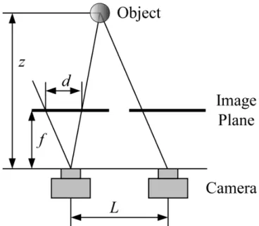
As said earlier, a single camera will generate a two dimensional representation of the world. This might be hard to believe as if a human views an image he/she can ”perceive” the missing dimension, depth. This is due to the human ability to interpolate by using visual features in the image. This is something a computer cannot do (yet) and hence it is unable to perceive depth from a single image. By using more than one camera, depth images can be created. The concept is presented in figure 2.1 by using a stereo-camera system.
The distance, z, to an object can be calculated by the formula seen in equation 2.1
z = (f L)/(pd) (2.1) by a method called triangulation. L is the distance between the two cameras, f is the focal lengths of the cameras, p is the size of one pixel in the cameras and d is the so called disparity. The disparity is the absolute value of the difference in pixels between the center of the object (or some other visual feature) between the two cameras. The same concept of triangulation used here is used in, for example, the Global Positioning System (GPS) where the position of a device is calculated by measuring the time it takes for signals to travel from a number of different satellites to the device. An example of stereo vision can be found in the work of Chen et al. [17]
Some main ideas are common for all computer vision systems. Firstly, representation of the environment must be acquired. Image acquisition can be done in many different ways with the most common one method is using a regular camera. Other ways of creating representations of the environment include LIght Detection and Ranging (LIDAR) and ultra sonic range sen-sors. After an image has been acquired some kind of filtering known as preprocessing is often performed in order to remove noise or unwanted part of the image. For example, if one wants to find green objects it would be unnecessary to keep anything but green pixels in the image. After the filtering is completed, an algorithm for feature extraction is often performed. After
Figure 2.1: Figure showing the concept of an stereo-camera setup taken from the work of Ohmura et al. [55]
relevant features are extracted the detection of some parameter is performed and the results used to control the system in some fashion. An example of such a video processing flow can be seen in figure 2.2. Other steps can be added as needed to the video flow in order to perform more complex operations.
Figure 2.2: Video flow example.
One example of filtering can be seen in figure 2.3 while one example of feature extraction can be seen in figure 2.4.
A common method for performing these image operations efficiently are by using a so called pipeline. Pipe-lining is a well known technique with the field of computer architecture and is used to increase throughput and parallelism in computer systems. The concept presented in figure 2.2 can be implemented as a pipeline. The essential idea between pipe-lining is to allow multiple instructions to overlap in execution, i.e. instead of performing all necessary operations in one stage the operations on data can be split between several stages that are interconnected. One good example of a pipeline implementation is the one found in Microprocessor without Interlocked Pipeline Stages (MIPS) pipeline where instructions have 5 distinct steps [32]:
1. Fetch instruction (IF) 2. Decode instruction (ID)
3. Execute instruction operation (EX) 4. Access operands (MEM)
5. Write result to register (WB)
An example of this pipeline can be seen in figure 2.5. For more information about the use of pipelines in modern computer architecture and the MIPS-pipeline, please refer to the works of Patterson and Hennessy. [32] [31]
Figure 2.3: Filtering example fromhttp://rsbweb.nih.gov/ij/plugins/sigma-filter.html
Figure 2.4: Feture extraction example from http://www2.cvl.isy.liu.se/Research/Robot/ WITAS/operations.html
A lot of pre-developed libraries that contain high-level image processing exist today. One example of such a library is the Open Computer Vision library better known as OpenCV. OpenCV is a open-source project released under the BSD-license, meaning that it free to use even in commercial applications. OpenCV contains a vast range of image processing algorithms and can be run in both Windows and *nix-based operating systems (Linux, Mac and Android). For more information about OpenCV please refer to the official homepagehttp://opencv.org/. One possible application of computer vision is within agriculture as can be seen in the research article written by Segerblad and Delight. [21] The most interesting example from the work of Segerblad and Delight [21] is, according to the author if this report atleast, the work of Weiss and Biber [64]. Using a LIDAR-device the two scientists detected and mapped vegetation in fields onto a global 3D map. This LIDAR-device was mounted onto a mobile robot that traversed the fields. The solution showed promising results with a successful detection rate of maize plants, in a field, of 60 percent. A image showing the mobile robots used and the generated 3D map can be seen in figure 2.6.
More information about computer vision and its applications can be found in the book written by Szeliski. [61].
Introduction to Programmable Logic (PL)
Logic circuits can either be fixed or programmable. Programmable logic behaviour can be changed after manufacturing is completed while fixed logic has a static behaviour. PL has existed for over 50 years and is extensively used in both industry and academia. It offers developers and researchers a flexible and fast way to design and implement hardware. Complex
Figure 2.5: MIPS pipeline
Figure 2.6: Figure showing the mobile robot used by Weiss and Biber (left) and the output 3D map (right). The image is from the work of Weiss et al. [64]
Programmable Logic Device (CPLD) is one of the most commonly used architectures together with FPGA. Both technologies have their unique properties and different applications. In this report the focus will be on FPGAs and their particular applications. A overview of the CPLD and FPGA technologies can be found in the article by Brown et al. [16]
One of the most interesting aspects of the various types of existing PL-architectures is the possibility to perform tasks in true parallel unlike regular CPU-based systems that must run tasks in series. This means that some tasks can be performed much faster on PL-devices than on CPU-devices. Another appealing aspect is the possibility to reprogram these devices without loss of performance. This implies a lower development cost compared to regular ASIC-devices and also the possibility to correct potential hardware bugs after they are released to the market.
Field Programmable Gate Array-technology
Modern FPGAs were first introduced in the middle of the 1980’s by the American company Xilinx [26] but the concept can be traced back to the 1960’s. The first Xilinx FPGAs only contained a few thousand logic cells while modern FPGA Integrated Circuits (ICs) can contain several millions. The basic concept of the FPGA is to pack large amounts of logic blocks, memory blocks and other low-level hardware peripherals onto one IC and then using a large network of interconnections to ”glue” all components together. [24] In figure 2.7 this concept is demonstrated.
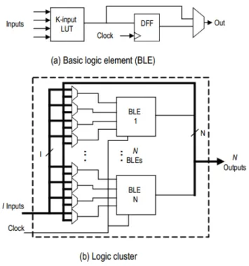
The high degree of interconnectivity is what makes the FPGA so versatile but is also one of the big drawbacks with FPGAs. The high degree interconnectivity implies that a large area of the FPGA-IC must be dedicated to this task, this increases the physical size of the packaging and also lowers the highest possible clock frequency as the clock signals must travel longer distances. Configurable Control Blocks (CLBs) provide the core logic and storage capabilities of the FPGA. In the figure 2.7 these are labelled just ”logic”. Today, most commercial CLBs are LUT-based. Each CLB consists of several Basic Logic Elements (BLEs) arranged in a special fashion. In Xilinx’s FPGAs a CLB consists of a number of so called slices which they consist of several BLEs. A BLE contains a N-input LUT and a D-type-flip-flop. Using a N-input LUT
Figure 2.7: Figure showing the general concept of an FPGA-device. The figure is from the article by Kuon et al. [48]
makes it possible to implement any logic functions with N-input bits. This concept is seen in figure 2.8. By connecting the output from the LUT to a D-flip-flop the behaviour of the circuit can become synchronised. More complex logic functions are implemented by connecting several of BLEs together. An example of this can be seen in figure 2.11 and also in 2.9. Most basic digital electronic concepts are explained in the book by Kuphaldt. [49]
Figure 2.8: Figure showing a typical LUT. [49]
The programming of the FPGA is basically just connecting the CLBs in the right fashion. Several different programming methods exist with some being static while others changeable. The most common one today is the use of some kind of static memory to hold the configuration while older technologies used fuses and anti-fuses to create permanent connections.
HDLs were created in order to increase the development speed of implementations on FP-GAs. Using a synthesis tool the HDL code is then translated into a bit stream containing the configuration of the FPGA. This bit stream can then be uploaded to the FPGA from a com-puter or dedicated programmer. The two most popular HDLs are Verilog and VHDL. Both are commonly used within both academia and industry. In later years graphical development tools for embedded systems on FPGAs have been released by most FPGA-manufacturers enabling developers to rapidly develop complex systems.
Figure 2.9: Picture from lecture slides from NTU. [8]
Figure 2.10: Figure showing how a LUT can be ”programmed” to perform logic operations. [49]
Run-time Reconfigurability of FPGAs with focus on the Xilinx
FPGAs
Many of the modern FPGAs support run-time reconfigurability to some extent, with partial reconfiguration being the most common one. Partial reconfiguration is a term commonly used when referring to reconfiguration of a specific part of the FPGA without interfering with other components located on the FPGA. As can been seen in the Introduction, partial reconfiguration can be dangerous to the overall system performance or stability if performed wrongly. The potential benefits of run-time reconfiguration are many, for example, the ability to dynamically move demanding functionality from software to hardware would improve performance of many applications. However, one must consider the time it takes to reconfigure a section on the FPGA and weigh that against the potential speed-up. Even tough the possibility of run-time reconfiguration has existed for over 2 decades now few FPGA manufactures have yet to provide a complete design flow including design tools and paradigms. Several reasons behind this can be found: The main reason is that the number of logic blocks on FPGAs have increased rapidly during this time and hence no direct need for partial reconfiguration has existed due to the much easier process of implementing a fully static system instead of using function swapping. Another reason is the added development time needed for the implementation and verification of systems that feature partial reconfiguration. However, as the ICs grow larger so does the time needed to
Figure 2.11: Figure showing the general concept of an FPGA-device. The figure is from the article by Kuon et al. [48]
program these. This proves to be troublesome in applications where start-up timing is crucial, as will be seen later in this section. Another implication is high static power consumption due to the increased number of transistors in each package. By utilizing smaller FPGAs in combination with partial reconfiguration lower power consumption and, in some cases, higher performance can be achieved.
In the book on the subject [44] Koch presents some crucial ideas behind the concept of partial reconfiguration. Koch separates between active and passive partial reconfiguration, where active reconfiguration is when the FPGA is reconfigured during run-time without disturbing the rest of the FPGA and passive reconfiguration is when the entire FPGA is stopped (stopped in this case is when all the clocks in the FPGA are stopped for a period of time) during reconfiguration. In this paper only active partial reconfiguration is considered and hence will be used synonymously with partial reconfiguration. Furthermore, Koch presents three open questions on the subject of partial reconfiguration that can be seen in the quote below. [44]
1. Methodologies: How can hardware modules be efficiently integrated into a sys-tem at runtime? How can this be implemented with present FPGA technol-ogy? And, how can runtime reconfigurable systems be managed at runtime? 2. Tools: How to implement reconfigurable systems at a high level of abstraction
for increasing design productivity?
3. Applications: What are the applications that can considerably benefit from runtime reconfiguration?
Furthermore, Koch identifies three possible benefits of partial reconfiguration: Performance improvement, Area and power reduction and fast-system start-up. To summarize: As has been stated before in this report algorithms that are highly parallel in nature can easily achieve speed-up by running on an FPGA compared with a CPU. By swapping functions in and out of the FPGA dynamically the power and area used can be reduced. Lastly, fast system start-up refers to systems where the device must have low start-up times. Partial reconfiguration can be used here to only load crucial components on the FPGA on start-up in order to minimize the start time and then at a later stage load the rest of the functionality on to the FPGA.An example of
this can be found in Xilinx Application Note 883 where a FPGA connected to the Peripheral Component Interconnect (PCI)-Express bus is partially configured at boot-up in order to meet the strict timing constraints of the bus. [62]
The partial reconfiguration methods can generally be divided into two categories: difference based reconfiguration for small net list changes and module reconfiguration for large module-based changes. This report will focus on module reconfiguration but according to Xilinx their latest FPGAs ”[..] support reconfiguration of CLBs (flip flops, look-up tables, distributed Ran-dom Access Memory (RAM), multiplexers, etc.), block RAM, and Digital Signal Processor (DSP) blocks, plus all associated routing resources.” [23]. This would imply that a high level of granularity can be achieved during difference based partial reconfiguration.
Partial reconfiguration can be seen as a specific implementation of context switching. How-ever, as Koch points one must consider the entire system state before explicitly labelling partial reconfiguration as context switching. [44]
Some key words used in the context of partial reconfiguration is needed to be explained and elaborated on before a more technical discussion of partial reconfiguration can occur. A short summary of commonly used terms are presented below and are a summary of the terms introduced and described both by Koch [44] and by Xilinx [35].
Reconfigurable Partition A physical part of the FPGA constrained by the user to host re-configurable modules.
Reconfigurable Module A net list that is set to reside inside a reconfigurable partition at some point. Several modules can share the same reconfigurable partition.
Reconfigurable Logic Logic elements that make up the reconfigurable module. Static Logic Logic implemented in such a way that it is not reconfigurable.
Proxy Logic Logic inserted by design software in order to provide the system with a known communication path between static logic and reconfigurable partitions.
The techniques for placement and interaction of/with reconfigurable modules within recon-figurable partitions differs between manufactures but three of the most common ones are: island style, grid style and slot style. Island style is the simplest model for partial reconfiguration and is the only one supported by Xilinx so far and hence it will be the focus of this report. A figure showing the concept behind island style placement can be seen in figure 2.12.
Notice the static region around the reconfigurable module. This is needed in order to provide a safe and efficient way for routing signals in and out of the reconfigurable module. The static region is extra important when the reconfigurable module is connected to a bus as it makes sure that the bus is not disturbed during reconfiguration. In Xilinx FPGAs the must common implementation of the static region was so called bus macros that was needed to be added manually by the user in the Integrated Software Environment (ISE) tool suite during the design phase. These have since been replaced by proxy LUTs that are automatically inserted during the synthesis. Island style placement only allows for one reconfigurable module per island. This means that a certain degree of fragmentation will occur when swapping modules as resources within the island will be wasted if not all resources are used by the new module. This is further enhanced by the fact that reconfigurable partitions must be predefined by the user and hence finding a perfect partition size in order to avoid fragmentation may be hard if not impossible. Furthermore, the current tools on the market require net lists to be generated for unique pair of module and island. This means that even if the same module can be placed in two different islands, two net lists and bit streams must still be generated. For example, a system that has 6 modules and 3 islands where all modules can resist in any island must have 18 unique net lists and bit streams. This is clearly time consuming for the designer.
Xilinx states in their user guide for Partial Reconfiguration, [35] that all logic can be recon-figured during run-time except: ”Clocks and Clock Modifying Logic [...], I/O and I/O related
Figure 2.12: Figure showing a typical island style partition location strategy.
components [...], Serial transceivers (MGTs) and related components [...] and Individual archi-tecture feature components (such as BSCAN, STARTUP, etc.) must remain in the static region of the design”. Further, it is stated that bidirectional interfaces between static logic and recon-figurable logic are not allowed unless explicit routes exist. Also some specific IP components might function erratically if used in combination with partial reconfiguration. Another design consideration to notice is that the interface between the reconfigurable partition and the static logic must be static, as stated earlier, this implies that all reconfigurable modules that is to reside within a reconfigurable partition must have the same interface ”out towards” the rest of the FPGA. Ports or bus connections cannot be created on the fly. An extensive list of design considerations for partial reconfiguration can be found in Xilinx UG702. [35]
In order to use partial reconfiguration on an Xilinx FPGA one must use their design suite ISE. The work flow to generate and use partial reconfiguration on a Xilinx FPGA using the Xilinx ISE will be presented in the method-chapter of this report. A general idea of the partial reconfiguration concept on a Xilinx FPGA can be seen in figure 2.13. The concept is in depth explained in work by Khalaf et al. [43] Designers are forced to use so called ”Bottom-Up-Synthesis” in order to successfully implement a reconfigurable system. This implies that all modules must have separate net lists for each possible instantiation and no optimization is allowed for the interface between the module and rest of the FPGA. Bottom-Up-Synthesis is explained in the Partial Reconfiguration Guide by Xilinx [35] and the Hierarchical Design Methodology Guide by Xilinx. [34]
Xilinx states the following design performance in UG702 [35]:
• Performance will vary between designs but in general expect 10% degradation in clock frequency and not to be able to exceed 80% in packing density.
• Longer runtimes during synthesis and implementation due to added constraints. • Too small reconfigurable partitions may result in routing problems.
From the user-side, reconfiguration of the FPGA during run-time is only a matter of writing a partial bit stream to the associated reconfiguration port. The most commonly used recon-figuration port in Xilinx-based systems are the ICAP-interface which can be instantiated as a
Figure 2.13: Figure showing the outline of the Xilinx RP. [35]
soft IP-core in the FPGA-fabric. Other reconfiguration interfaces such as the ZynQ’s Parallel Configuration Access Port (PCAP)-interface exists as well. This report focuses on the actual us-ability of the partial reconfiguration flow and the technical low-level reconfiguration process will hence not be discussed here. A good introduction to the partial reconfiguration work flow and limitations for Xilinx FPGAs can be found in Partial Reconfiguration User Guide by Xilinx. [35] Xilinx claims the following in the Partial Reconfiguration Reference Design for the Zynq [46]:
The configuration time scales fairly linearly as the bitstream size grows with the number of reconfigurable frames with small variances depending on the location and the contents of the frames.
If the reconfiguration time is linear with respect to the bitstream size it would imply that partial reconfiguration could be used in time-critical systems as the worst case scenario could be calculated and verified with a high degree of certainty. This property could be useful in high-speed applications such as video processing or other streaming data applications.
An article from 2006 written by Xilinx employees describes the general work-flow in their ISE-tool-suite and much of the information found there still applies to the current versions. [52]
Heterogeneous systems
A general trend in both research and industry is to use more and more heterogeneous systems. Heterogeneous systems are composed of several different processing architectures. An example of this is the Xilinx ZynQ-platform which features two hard ARM-cores and a large FPGA-section in one IC. The Xilinx ZynQ-family of FPGAs will be discussed later in this chapter. Another example of a heterogeneous system can be seen in the Related Work-section of this report, more precisely the work of Blair et al. [14].
Heterogeneous systems enables programmers to utilize different processing architectures dif-ferent properties for difdif-ferent tasks. For instance, a task that can be run in parallel can be put on an FPGA while a strongly serial task can be run on the much faster CPU. However, these systems are not without drawbacks. Different processing architectures use different methods of execution and tasks must be adapted to fit these methods in order work correctly.
Computer Vision on FPGAs and heterogeneous systems
The parallel nature of FPGAs makes them ideal for running image processing algorithms due to the outline of these algorithms. An example of this is the conversion between the YUV422-color format and the RGB-color format. The equation for the conversion can be seen in equation 2.2.
R G B 1 0 1.13983 1 −0.39465 −0.58060 1 2.03211 0 Y U V (2.2) If the simple conversion example seen in equation 2.2 would be run in series it would require at least
P ictureW idth ∗ P ictureHeight iterations to finish. For an image in the VGA-format (640x480 pixels) 307200 iterations are then needed. If this conversion would be implemented on an FPGA all pixels could be converted at the same time in parallel, that is only a few iterations would be required (assuming that the entire picture is available in the FPGA component at the start of the conversion process, which rarely is the case). One example if this can be found in the work of Hamid et al. [29] where a filtering algorithm that took 17 iterations to finish on a CPU only took 5 iterations on an FPGA.
Integrating hard processor cores in to FPGAs is no new idea, however. For example, previous Xilinx FPGAs have featured PowerPC-processors integrated into them (Virtex-IV) and a wide range of soft CPU-cores exist for integrating in the FPGA-fabric, such as Microblaze from Xilinx and NIOS from Altera. Using heterogeneous systems for video processing have several positive implications for the overall system performance and usability as will be seen later in this report.
Xilinx ZynQ-7000 and Xilinx XC702
This thesis focuses on using partial reconfiguration of the Xilinx ZynQ-7000 FPGA family. Hence, it is important to discuss the features and properties of these devices and especially present the development boards used, the Xilinx ZC702 and GIMME2 that will be presented in the next section. Xilinx calls the ZynQ family for a EPP-family due to the fact that it both features a ARM-processor and a FPGA-block in the same package. The general idea of using the EPP is demonstrated in figure 2.15.
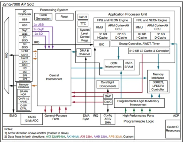
An outline of the Xilinx ZynQ-SoC can be seen in 2.16 and a table showing some of the basic characteristics of the different devices in the ZynQ-family can be found in Appendix B. The ZynQ can generally be divided into two different regions: the PL featuring the FPGA-fabric and the Processing System (PS) featuring the ARM-processor. The Xilinx ZynQ SoC features a wide range of embedded peripherals. The most interesting ones for report are the DevC-interface (Where the PCAP-interface is located) and the Advanced eXtensible Interface (AXI)-bus between the PL and the PS. The AXI bus is a high-performance bus developed and specified by ARM. It provides developers with an easy way of interfacing between the PL and the PS-sections. The principal layout of the DevC-module of the Advanced RISC Machine (ARM)-processor on the Zynq can be seen in figure 2.14.
The latest version of the AXI bus, version 4, have three distinct implementation: AXI4, AXI4 Lite and AXI4-Stream. The standard AXI4 bus is a burst based master-slave bus with independent channels for read addressing, write addressing, data reception, data transmission and transmission response. The width of the data channels can range from 8 upto 1024 bits. Interconnects are used to connect masters to slaves, and vice versa, and several masters can be connected to the same interconnect. AXI4-Lite is a reduced version of the standard AXI4 bus designed for a more simple communication method between masters and slaves that is not capable of burst reads or writes. The width of the buses are also limited to either 32 or 64 bits. AXI4-Stream is a stream based communication interface that is designed for high-performance applications such as video processing. As AXI4-Stream is stream based, it lacks the address channels present in regular AXI4. AXI4-Stream can either be used as an direct protocol where
Figure 2.14: The layout of the DevC-module. [38]
a master units writes directly to a slave unit or together with an interconnect in order to perform operations on the data stream such as routing or resizing. In order to pass stream based data into a memory an extra component is needed and a common technique is to utilize an DMA-device to perform such operations without the direct involvement of the processing unit. This is common with video applications where frame buffers are used to store video frames between the various stages of the video pipeline. More information about the regular AXI4-protocol and AXI4-Lite can be found in the specification supplied by ARM. [6] More information about the AXI4-Stream-protocol can be found in the specification released by ARM. [5]
The Xilinx ZynQ has integrated AXI-based high performance ports for PL access of the memory connected to the PS. This allows the two different sections to share memory. Further-more, other AXI-based ports are available for communication and peripheral sharing between the PS and PL sections. Also interrupts and Extended Multiplexed I/Os (EMIOs) are routed between the PL and the PL. More extensive information about the Xilinx Zynq SoC can be found in the Technical Reference Manual [38].
Xilinx ZC702 is a development board featuring a Xilinx ZynQ XC7Z020 SoC and wide range of on-board peripherals. A picture showing these various peripherals can be seen in 2.17
GIMME 2
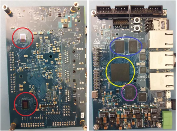
GIMME2 is an computer vision platform developed by professor Lars Asplund at M¨alardalen University and AF Inventions GmbH. The board features, for example, a Xilinx ZynQ XC7Z020-2 SoC, two Omnivision OV10810 10-Megapixel image sensors and separate DDR-memories for the PL and the PS. A short technical summary of the board can be seen in figure . The board itself can be seen in the figure . The GIMME2 platform is intended to function as a research platform for researchers at M¨alardalen University and other research institutes as well.
Figure 2.15: Figure showing the general idea on how to utilize the Xilinx EPP-family. [41]
Figure 2.16: Figure showing the outline of the Xilinx ZynQ-SoC. Image from Xilinx document UG585. [38]
Figure 2.17: Figure showing the ZC702 board peripherals. [41]
Figure 2.19: Figure showing the GIMME2 boards front (right) and backside (left). Notice the two image sensors on the backside of the PCB (encircled in red). Also notice the Zynq SoC (encircled in yellow, the PS DDR Memory (encircled in blue) and the PS DDR Memory (encircled in purple).
Related work
Implementations of computer vision on FPGAs and
heteroge-neous systems
Utilising the computational power of an FPGA in a mono or stereo vision system is no new concept. This concept has been the target of many researcher’s work throughout the years, for reasons already accounted for. One interesting, and relevant to this report, implementation of computer vision on an FPGA is the work of Hosseini and Hu [29]. Hosseini and Hu compared the performance of a hard logic solution against a soft CPU-core (Altera Nios II) implemented on an FPGA when given the task to filter a 64 x 64 pixel or 256 x 256 pixel grey scale image using a n x n coefficient matrix. It was found that the logic FPGA-implementation was immensely faster than a similar implementation on a CPU. The authors found that the logic based solution could perform up to 80 times faster. The results of this article can be seen in figure 3.1.
Table 3.1: Figure showing the results from work by Hosseini and Hu. [29] The first four rows are for the filtering of a 64 x 64 pixel image while the last two are for the filtering a 256 x 256 pixel image.
An overview of the algorithm implemented in hard logic and the algorithm implemented on the soft CPU-core by Hosseini and Hu can be seen in figure 3.1.
Another implementation of a computer vision system on an FPGA can be found in the article by Ohmura and Takauji. [55] Ohmura and Takauji used a stereo-vision system with the Orientation Code Matching (OCM) algorithm running on an Altera FPGA-chip. In short, the OCM algorithm is designed to find similarities between pictures and one possible application is stereo-machining. An extensive explanation of the OCM algorithm can be found in the same paper. The stereo vision module used was capable of supplying images by the size 752 x 480 pixels at 60 FPS. The FPGA on module was an Altera Cyclone III running at 53 MHz. A figure showing a block diagram of the developed system can be seen in figure 3.2. The implemented system performed with a minimal delay but used 82% of the available Logic Elements on the FPGA. The system used a 16 x 16 pixel template size with a maximum disparity of 127 pixels. A overview of the algorithm implemented on the FPGA can be seen in figure 3.3.
Figure 3.1: Figure showing the system from the article by Hosseini and Hu. [29] To left is the logic implementation and to the right is the CPU implementation using the Altera Nios II.
Figure 3.2: System developed by Ohmura and Takauji. Picture is retrieved from the article by Ohmura and Takauji. [55]
heterogeneous system featuring a microprocessor and an FPGA. They developed a high-speed system capable of retrieving 1000 FPS using a single camera setup. The architecture used can be seen in figure 3.4. The camera used were capable of outputting 1280 x 512 pixel frames at 1000 FPS. By splitting functionality between the CPU and the FPGA the team managed to get acceptable performance out of the system. The implemented system, with the CPU running at 266 MHz and the FPGA at 200 MHz, was compared to an PC with a dual-core Intel processor running at 1.86 GHz and with 3 Gb of RAM. On the PC OpenCV was used to provide high-level image processing capabilities. In figure 3.2 a comparison between similar functions running on the heterogeneous system and on the PC can be seen. It is quite clear that even though the clock frequency of the heterogeneous platform is much lower, it still can outperform the dual-core PC in most of the cases due to the increased level of parallelism achieved.
Blair et al. [14] present a vision system implemented on a heterogeneous platform (GPU,FPGA and CPU) for detection of pedestrians in real-time using a algorithm called HOG (Histogram of Oriented Gradients). Shortly, HOG works by looking at the intensity gradients of image pixels and then uses this data to detected objects. Blair. et al.’s system was based around an dual-core Intel processor running at 2.4 GHz, a Xilinx Virtex-6 FPGA and a Nvidia 560Ti Graphics Processing Unit (GPU). The devices were connected together using the PCI Express-bus. Each stage of the implementation can run on any of the processing units and mixing between the different architectures are allowed. Figure 3.5 shows the possible paths data can take. The per-formance of the system was evaluated by sending two 1024 x 768 pixel images through all the different data paths. One of the images were single scale and the other had 13 scales. The fastest data path, for both images, was the one mainly using the GPU, 6.8 ms and 47.0 ms, while the
Figure 3.3: System developed by Ohmura and Takauji. Picture is retrieved from the article by Ohmura and Takauji. [55]
Figure 3.4: Komuro et al.’s architecture. [47]
slowest one was the one mainly using the CPU, 174.3 ms and 1376 ms. Using mainly the FPGA gives the third best times, 10.1 ms and 124.5 ms. The authors conclude that communication delay is a major problem and combining two processing units in one data flow is not preferred due to this. Furthermore, Blair et al. state that it would be better to, instead of splitting the algorithm between processing units, dedicate each processing unit to a specific task and then combine the results of each task in the end.
For more information about the implementation and design of computer vision systems on FPGAs please refer to the comprehensive book on the subject by Bailey. [9] An overview of the state of the art in heterogeneous computing can be found in the work by Brodtkorb. [15]
Implementations of reconfigurable FPGA-systems
Thoma et al. [63] discusses a method for dynamic pipeline reconfiguration of a soft core processor implemented on an FPGA. Thoma et al. present a novel processor core that can be reconfigured with respect to the depth of the pipeline in order to increase performance of decrease power consumption. The processor core is based upon an already existing one called LEON3. LEON3 is implemented in VHDL and can hence be used on a FPGA. For more information about LEON3, please refer to the technical paper about LEON3. [1] By cleverly joining or splitting up adjacent pipeline stages dynamically, Thoma et al. demonstrated a relative saving of 3,8% in cycle count over the execution of a test program.
In master thesis by Hamre [30] a framework (in principle a hardware operating system) is presented for dynamic reconfiguration of FPGAs. Hamre’s work is closely related to the work present in this report as the same principal ideas are shared. Hamre thoroughly presents the concept of partial reconfiguration and also the difficulties of implementing it. Hamre’s framework is designed to work with Linux and also uses the Xilinx ICAP-port for reconfiguration. The
Table 3.2: Komuro et al.’s performance. [47]
Figure 3.5: Blair et al.’s performance. [14]
results show that partial reconfiguration of an FPGA from Linux is possible with the available tools. However, no real performance evaluation is made in Hamre’s report.
In the article by Lesau et al. [50] the usage of real-time reconfiguration in combination with embedded Linux is discussed and furthermore a set of tools for easier handling of reconfiguration is presented. Lesau et al. have successfully implemented tools like mail-boxes for Linux to hard-ware module communication and also a hardhard-ware administrator that handles reconfiguration. This system was implemented on an Xilinx Virtex-5 FPGA using MicroBlaze-cores and PetaL-inux. Lesau et al. successfully proved that this kind of hardware and software layout could be used for handling dynamic reconfiguration.
Meyer et al. present a new configuration method for FPGAs in their article on the subject. [53] The researchers have named it ”Fast start-up”. By manipulating the bit streams generated the regular development tools, Meyer et al. significantly decreased the configuration time of a Xilinx Spartan-6 FPGA. The results from these tests can be found in table 3.3.
In Ming et al. [51] a comparison between different ICAP-components are made and the reconfiguration speed versus the bit-file-size are compared. They found that by making radical
Table 3.3: Meyer et al.’s results. [53]
changes to the standard ICAP the reconfiguration time could be lowered by a order of one magnitude. Ming et al.’s results (reconfiguration time versus file size) can be seen in table 3.4. In figure 3.6 one can see the almost linear relationship between bit file size and reconfiguration time.
Table 3.4: Table showing Ming et al.’s results taken from their article. [51]
In the work by Koch et al. [45] present the concept of partial reconfiguration and also demon-strates some tools commonly used for achieving it. Furthermore, some possible applications of partial reconfiguration is presented to the reader with one application being a ”self-adaptive reconfigurable video-processing system”. This implemented system can be seen in figure 3.7. The modules seen in the picture can be dynamically loaded and unloaded during run-time. This system was implemented on an Xilinx Virtex-II FPGA. No performance indicator is given but it would appear as the performance of the system is acceptable for non-real time applications, thus proving that the concept is implementable. Koch has also published a book on the sub-ject named ”Partial Reconfiguration on FPGAs” which may be of interest for the reader. [44] Koch is also the co-author of the article where the GoAhead-tool for partial reconfiguration is presented. [10] GoAhead is aimed to provide developers with a simple user-interface in order to create systems containing reconfigurable modules.
Several other tools and work flows have lately emerged for creating run-time reconfigurable systems. For example: Dreams [56], the work by Ruiz et al. [54] and the work by Dondo et al [22].
Gantel et al. [27] discuss a possible algorithm for module relocation during run-time. The work was performed on a Xilinx FPGA mostly using the Xilinx tool Isolation Design Flow. The main problem when dealing with relocation of modules on an FPGA is that each module must have an unique bit-stream for each possible module location on the FPGA. Gantel et al. want to make it possible to only have one bit-stream per module and then using a bit-stream parser and bit-stream re-locator just adapt so that the module can be placed anywhere on the glsFPGA. This would allow for a more efficient design. Gantel et al. succeeded with module relocation on
Figure 3.6: Figure showing Ming et al.’s results taken from their article. [51] the FPGA with their proposed method.
Garcia et al. [28] presented a possible application of reconfigurable FPGAs within Wireless Sensor Networkss (WSNs).
In the work by Papadimitriou et al. [57] the authors present their solution of providing fast reconfigurations and also propose a model for cost estimation of the reconfiguration process.
Implementations of reconfigurable FPGA-systems running
com-puter vision algorithms
Ackermann et al. [2] implemented a self-reconfigurable video processing system on an FPGA. They present two different implementations of the system. In the first one a Xilinx Virtex-IV FPGA is used and reconfiguration was performed with the help of the ICAP and a Microblaze-processor. Some common image processing algorithms were implemented as modules used for the reconfiguration testing. The first image processing algorithm implemented was binarization, the second was edge detection using 2-d gradients and the third one was edge detection using horizontal derivative. The bit-streams are here stored on a CompactFlash-card accessed from the MicroBlaze processor. Image data is retrieved from an camera with a resolution of 2048 x 2048 pixels at 16 Frames Per Second (FPS). For both implementations only one image processing algorithm was allowed on the FPGA. An overview of the first implementation can be seen in figure 3.8. In the second implementation, the MicroBlaze processor has been removed and been replaced by a small bit-stream controller connected to a Static Random Access Memory (SRAM)-memory where all bit-streams are located. The results of the two different implementations can be found in figure 3.6 which shows the time needed to reconfigure the FPGA. The size of each implemented processing algorithm can be found in 3.5. This clearly shows that run-time reconfiguration is possible even in such demanding systems as video processing systems.
Another implementation of a dynamic reconfiguration in a multimedia application was pre-sented in the work by Bhandari et al. [11] Bhandari et al. used a Xilinx Virtex-4 FPGA to implement a test-platform where a VGA-camera stream was fed into the FPGA, past a recon-figurable filter module and then outputted onto a monitor. Also available on the FPGA was an audio module that also had a reconfigurable filter slot. Three programming techniques
uti-Figure 3.7: Koch et al.’s implemented system. Picture is taken from the related article. [45]
Table 3.5: Ackermann et al.’s results. [2]
lizing the ICAP were tested. The first two, OPB-HWICAP and XPS-HWICAP, are made by Xilinx while the last one, SEDPRC, is designed by Bhandari et al. The results of these tests can be seen in figure 3.7. As can be seen the novel ICAP interface performs much better than the Xilinx alternatives, hence performance of the ICAP-interface can be improved by utilizing custom-made components.
A run-time reconfigurable ”multi-object-tracker” were implemented by Perschke et al. [58] The system implemented is based on a Xilinx Virtex 4 FPGA with a PowerPC-CPU and video is retrieved from a camera running at 384 x 286 pixels and 25 FPS. Just like Bhandari et al., Perschke et al. have implemented a new ICAP-controller in order to improve performance of the system as the standard Xilinx ICAP-controller was deemed to slow to be used. In figure 3.8 the total usage of each component implemented can be seen. In figure 3.9 the results from the article can be found. Perschke et al. conclude that components can be switched between frames and hence no delay in the object-tracking algorithm is produced. Looking at the resource utilization of the components used and the speed of the switching it can be concluded that this method can be used in high-speed vision systems.
A application for partial reconfiguration within the automotive industry can be found in workings by Claus et al. [18] [19] These studies shows that FPGAs and real-time reconfiguration


![Figure 2.18: Figure showing the outline of the GIMME2 platform. [3]](https://thumb-eu.123doks.com/thumbv2/5dokorg/4705205.123812/31.892.197.720.741.1088/figure-figure-showing-outline-gimme-platform.webp)