Linköping Studies in Science and Technology Licentiate Thesis No. 1537
HiPIMS-based Novel Deposition Processes for Thin Films
Asim Aijaz
LIU-TEK-LIC-2012:22
© Asim Aijaz 2012
ISBN: 978-91-7519-870-5 ISSN 0280-7971 Printed by LiU-tryck Linköping, Sweden, 2012
Abstract
In this research, high power impulse magnetron sputtering (HiPIMS) based new deposition processes are introduced to address; the issue of low degree of ionization of C in magnetron sputtering discharges, and the difficulty encountered in thin film deposition on complex-shaped surfaces. The issue of low degree of C ionization is addressed by introducing a new strategy which is based on promoting the electron impact ionization of C by increasing the electron temperature in the plasma discharge using Ne, instead of conventionally used Ar. The Ne-based HiPIMS process provides highly ionized C fluxes which are essential for the synthesis of high-density and sp3 rich amorphous carbon (a-C) thin films such as diamond-like carbon (DLC) and tetrahedral a-C (ta-C). The feasibility of coating complex-shaped surfaces is demonstrated by using the dual-magnetron approach in an open-field (magnetic field of the magnetrons) configuration and performing sideways deposition of Ti films. The HiPIMS-based open-field configuration process enhances the sideways transport of the sputtered flux — an effect which is observed in the case of HiPIMS.
The characterization of the Ne-HiPIMS discharge using a Langmuir probe and mass spectrometry shows that it provides an increase in the electron temperature resulting in an order of magnitude decrease in the mean ionization length of the sputtered C as compared to the conventional Ar-HiPIMS discharge. The C1+ ion energy distribution functions exhibit the presence of an energetic C1+ ion population and a substantial
1+ 1+ 3
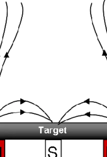
The dual-magnetron open-field configuration process is operated in DCMS as well as in HiPIMS modes. The plasma characterization, performed by Langmuir probe measurements and optical emission spectroscopy, shows that the plasma density in the Ti-HiPIMS discharge is higher than that of the Ti-DCMS discharge. This results in the higher ionized fraction of the sputtered Ti in the case of HiPIMS. The film uniformity and the deposition rate of the film growth, obtained by employing scanning electron microscopy, demonstrate that the sideways deposition approach can be used for depositing thin films on complex-shaped surfaces.
Preface
This Licentiate Thesis is a part of my PhD studies in the Plasma and Coatings Physics Division at Linköping University. The goal of my doctorate project is to develop new magnetron sputtering based processes which facilitate the synthesis of DLC and ta-C at laboratory as well as at industrial scale. The research is financially supported by the Swedish Research Council (VR) through the contracts 621-2008-3222 and 621-2011- 4280.
Appended Papers
1. A strategy for increased carbon ionization in magnetron sputtering discharges
Asim Aijaz, Kostas Sarakinos, Daniel Lundin, Nils Brenning and Ulf Helmersson
Diamond & Related Materials, 23 (2012) 1.
2. Dual-magnetron open field sputtering system for sideways deposition of thin films
Asim Aijaz, Daniel Lundin, Petter Larsson and Ulf Helmersson
Surface & Coatings Technology, 204 (2010) 2165.
Publications not included in the thesis
1. Patent: Sputtering process
Ulf Helmersson, Nils Brenning and Asim Aijaz Patent application (Approved) 2012.
2. A novel high-power pulse PECVD method
Henrik Pedersen, Petter Larsson, Asim Aijaz, Jens Jensen and Daniel Lundin Accepted for publication in Surface & Coatings Technology, 2012.
3. Effect of peak power in reactive high power impulse magnetron sputtering of titanium dioxide
Montri Aiempanakit, Ulf Helmersson, Asim Aijaz, Petter Larsson, Roger Magnusson, Jens Jensen and Tomáš Kubart
Surface & Coating Technology, 205 (2011) 4828.
4. Understanding the discharge current behavior in reactive high power impulse magnetron sputtering
Montri Aiempanakit, Asim Aijaz, Daniel Lundin, Ulf Helmersson and Tomáš Kubart
In manuscript.
5. Deposition of yttria stabilized zirconia thin films for solid oxide fuel cells by high power impulse magnetron sputtering and pulsed magnetron sputtering Steffen Sønderby, Asim Aijaz, Kostas Sarakinos, Ulf Helmerssonand Per Eklund In manuscript.
Acknowledgements
First of all, I would like to thank Almighty Allah, Who is the real source of knowledge and wisdom.
Furthermore, there are a number of people whose valuable contributions made this journey rewarding for me. I would like to extend my deepest gratitude towards them.
These are:
Ulf Helmersson, my main-supervisor, who gave me the opportunity to conduct this research and whose guidance, patience, encouragement and difficult questions, helped me to progress.
Kostas Sarakinos, my co-supervisor, whose passion and dedication for science is inspirational. I like to thank him for his support, encouragement, time and for guiding me to new directions in my research.
Daniel Lundin, for being supportive and encouraging co-worker, for providing great insights into the subject and for always showing the positive aspects of even the disappointing-looking outcomes.
All other members of the Plasma and Coatings Physics division, for creating an
My friends in Sweden and back in Pakistan, each of them is equally valuable for me.
All my family members, without their sacrifices, encouragement, support and prayers, I am nothing!
My soul mate, my wife, Yasra, who always brings sense of friendship and support to me.
In every moment that I spend with You, I live a life!
My Mother; the person behind all my success, the source of inspiration at all stages of my life, my reason to smile and whose contribution to my life can not be described in words.
Contents
Abstract I
Preface III
Acknowledgements V
Appended Papers VII
Publications not included in the thesis VIII
1 Introduction 1
1.1 Background and Motivation 1
1.2 Goals and Research Strategy 4
1.3 Outline 4
2 Plasma-Assisted Physical Vapor Deposition 5
2.1 Sputtering 5
2.2 Magnetron Sputtering 7
2.2.1 Direct current magnetron sputtering (DCMS) 8
2.2.2 High power impulse magnetron sputtering (HiPIMS) 8
3 Basic Plasma Physics 11
3.1 Introduction 11
3.2 Plasma for Material Synthesis 12
3.3 Ionization Processes 16
4 Amorphous Carbon Growth 21
5 Amorphous Carbon Growth and Ionized PVD 27
5.1 Filtered Cathodic Vacuum Arc (FCVA) 27
5.2 Pulsed Laser Deposition (PLD) 28
5.3 HiPIMS 29
6 Research Strategy and Experimental Details 31
6.1 Research Strategy 31
6.2 Plasma Characterization 32
6.2.1 Langmuir Probe Measurements 33
6.2.2 Mass Spectrometry 36
6.2.3 Optical Emission Spectroscopy 38
6.3 Film Characterization 40
6.3.1 X-ray Reflectometry 40
6.3.2 Scanning Electron Microscopy 42
7 Summary of the Appended Papers 43
8 Ongoing Work and Future Outlook 45
9 References 47
Paper 1-2 51
1. Introduction
1.1 Background and Motivation
Thin films are structures with thicknesses ranging from several nanometers up to several micrometers that are formed when atomic layers of a material are deposited on a surface to alter its properties and functionality [1]. The desired properties can be achieved by mono-elemental films (such as Au thin films are used as corrosion-resistant electrically conductive layers in electronic industry) [2] or films that consist of more than one elements (such as Al2O3 films are used as protective coatings for cemented carbide cutting tools) [3]. The ultimate goal of thin film science and technology is to develop tailor-made materials in such a way that they exhibit different attributes and hence they can be used in various applications. An example is amorphous carbon (a-C) films, which exhibit unique and adjustable properties ranging from those of graphite to those of diamond — finding their applications ranging from lubrication to ultra-dense hard coatings [4,5]. These properties are controlled by the hybridization state of the carbon atoms i.e. the ratio of the sp3 to sp2 hybridized bonds and the atomic H content [5]. On the basis of the atomic H content, a-C can be classified as H-free amorphous carbon (a-C) as well as hydrogenated amorphous carbon (a-C:H) [4,5]. Apart from H, the material can also adopt a large number of stable forms by bonding strongly to other atoms such as Si, N, B and F which leads to a wide range of carbon-based thin films and coatings [4].
Amorphous carbon-metal nanocomposites are another emerging material systems where metal atoms are incorporated into a-C matrix to tailor, for example, the electrical
Amorphous carbon thin films for specific applications are nowadays commonly synthesized by chemical vapor deposition (CVD) — where a vapor of the depositing carbon is created using chemical reaction of gases [5,8] — and physical vapor deposition (PVD), where the same is achieved through physical processes such as sputtering or evaporation from a graphite solid source (referred to as target) [5]. Both of these groups of methods are widely used for a-C synthesis at laboratory as well as at industrial scale.
The-state-of-the-art approaches for the synthesis of a-C using PVD methods include;
cathodic arc evaporation (CVA), pulsed laser deposition (PLD) as well as magnetron sputtering based methods, e.g. radio frequency magnetron sputtering (RFMS) [5,9]. CVA, PLD and RFMS are also termed as plasma-assisted PVD methods since in these methods, the vapor generation and transport to the substrate involve an assistance of plasma. The plasma for material synthesis is described in chapter 2.
In a plasma-assisted PVD method, the sp3/sp2 ratio — vital for the a-C film functionality
— can be controlled by the energy and the flux of the depositing species (carbon as well as the buffer gas species) [5,10]. The control over the energy becomes much easier if a large fraction of the depositing flux is ionized. In this case the energy of the depositing flux can be tuned by the use of an electric field, e.g. by applying a bias potential to the substrate (the place where the source material is deposited). Another important consideration with respect to the deposition of thin films (including a-C) is the geometry of the substrate. Often, the complex-shaped surfaces are encountered — e.g. engine valves covered by carbon-based wear-resistant coatings [11] — which makes it difficult to achieve uniformity in the coatings [12]. This difficulty can also be overcome by achieving highly ionized depositing fluxes, since electric and magnetic fields can also facilitate control over the direction of the ionized depositing flux [13,14].
The plasma-assisted PVD methods where more than 50% of the depositing material is ionized are called ionized PVD methods [15]. Both, CVA and PLD fall into this category since the ionized fraction of the depositing flux reaching up to 100% can be obtained using these methods thereby making the synthesis of dense and sp3 rich a-C thin films possible [5]. However, they exhibit some drawbacks such as macroparticle ejection from
the target, lack of lateral film uniformity and in some cases, are difficult to scale-up [16,17]. Magnetron sputtering-based methods overcome the drawbacks which are inherent to CVA and PLD and therefore, these methods are technologically more relevant.
However, highly ionized depositing fluxes cannot be created using conventional magnetron sputtering methods, such as direct current magnetron sputtering (DCMS) and RFMS [15]. For the case of a-C growth, this means that tailoring the properties of a-C thin films as well as the synthesis of dense and sp3 rich a-C using these methods is difficult [5,9].
An emerging magnetron sputtering based technique is high power impulse magnetron sputtering (HiPIMS) [11,18]. HiPIMS provides a substantially higher ionization of the depositing flux as compared to the conventional magnetron sputtering methods. HiPIMS has already demonstrated its potential as an ionized PVD method for most commonly used metals such as Cu, Ti, Ta, Al etc [15]. For example, an ionized fraction of more than 90% has been reported for Ti using HiPIMS [19]. The potential of HiPIMS for non- metals such as C, has not been fully explored and a limited research has been carried out for the synthesis of a-C using HiPIMS. In one report, DeKoven et al. showed that an ionized fraction of only 5% is achieved in C-HiPIMS discharges [20]. In another study by Sarakinos et al., it has been shown that using HiPIMS, the a-C films with mass densities reaching up to 2.2 gcm-3 and an sp3 fraction of 45% can be grown [21]. Moreover, the same study reported that the implementation of HiPIMS affects mainly the ionization of the buffer gas (Ar) atoms while the C ionization degree remains at the same levels as those achieved by the conventional DCMS processes. These results show that there is much room for the improvement in the conventional HiPIMS-based C discharges as well as there is a need for understanding and addressing the fundamental issue of low degree of C ionization in magnetron sputtering discharges. By addressing this issue, an industrially more relevant technique will be available for the synthesis of dense and sp3 a- C as well as it will facilitate the deposition of a-C coatings on complex-shaped surfaces.
1.2 Goals and Research Strategy
The first goal of this research is to understand and address the issue of low degree of carbon ionization in magnetron sputtering discharges — by using HiPIMS as the model magnetron sputtering based process — and grow high density and sp3 rich a-C coatings.
The goal is achieved by introducing a new strategy for increasing carbon ionization which leads to developing a new HiPIMS-based process. The strategy is based on increasing the electron temperature in the plasma discharge by using Ne as the sputtering gas, instead of conventionally used Ar. Both, the Ne-HiPIMS and Ar-HiPIMS discharges are operated under the identical process conditions and plasma characterization is performed to compare the resulting plasma properties. Carbon thin films are synthesized under various deposition conditions and the resulting film properties are also compared.
The second goal is to develop a HiPIMS-based process for the synthesis of thin films on complex-shaped surfaces to fully exploit the potential of the new HiPIMS process for real applications. This goal is achieved by using the dual-magnetron approach with an open- field configuration and performing sideways deposition of Ti films, when the magnetrons are operated synchronously in DCMS as well as in HiPIMS modes. Ti is chosen as a model system, owing to the higher degree of ionization of Ti, achieved in magnetron sputtering discharges, as compared to C. The plasma characterization is performed to investigate and compare the degree of ionization in the DCMS and HiPIMS processes.
Film characterization is performed to investigate the growth rate and the uniformity of the coatings.
1.3 Outline
The outline of this thesis is as follows: First, an overview of the sputtering-based methods is presented which is followed by a chapter on the basic plasma physics. After this, the fundamentals of a-C growth and state-of-the art of a-C growth are discussed. A chapter is included which describes in detail the research strategy and adopted methodology including experimental details — where the methods for plasma and film characterization are discussed. After this, the summary of the appended papers is presented and in the end, the thesis is concluded with the future outlook of the research work.
2. Plasma-Assisted Physical Vapor Deposition
As described in the previous chapter, there are various plasma-assisted PVD methods which are employed for the synthesis of thin films and coatings. Among these, the magnetron sputtering based methods are relevant to this work therefore, a brief description of commonly used magnetron sputtering based methods is provided in the following sections.
2.1 Sputtering
Sputtering is a physical process of ejecting the target atoms (source material) by means of an incident energy [1,22]. In a plasma based sputtering process, the incident energy is supplied via an interaction between the plasma constituents and the target atoms [22].
Sputtering plasma is the subject of the next chapter and here, a plasma can be considered simply as a collection of ions and electrons which is generated through an electrical discharge of an inert gas such as Ar [1]. Ions from the plasma are accelerated to the target by applying a negative potential to the target and as a result, various ion-solid surface interactions occur. These interactions can be influenced by many factors such as the incident ion energy, angles of incidence of the ions, binding energy of the target atoms, mass of the incident and target atoms etc., [22]. On the basis of the energy of the incident species, the process of sputtering is divided into three regimes of low (< 1keV), moderate (1-50 keV) and high energy (>50 keV), which are depicted in Figure 1 [22].
Figure 1. Energy regimes of sputtering: a) Single knock-on (low energy), b) Linear cascade (moderate energy) and c) Spike (high energy). (After P. Sigmund [22].)
In the low energy regime, the target atom which receives the incident energy at first place, through one-to-one interaction with the impinging ion, responds to it in an individual manner and therefore the process is referred to as the single-knock on [22]. In the moderate energy regime, the impinging atom can make a series of collisions with several target atoms thereby producing a cascade of ions along its path. The recoiled target atoms can be displaced from their sites in the solid and subsequently sputter out. This moderate energy regime is termed as the linear-cascade. In the high energy regime, the incident ion carries a substantially high energy which is enough to provide the binding energy to all atoms along its path. The condition of binary collisions (as is the case with the linear- cascade) no more holds and it is likely that the next atom which an incident atom interacts with, is already in motion. This regime is referred to as the spike [22].
The energies of the sputtered target atoms follow the Thomson distribution while they spread out according to cosine distribution [22]. The sputtered atoms traverse through the bulk plasma and thereby condense onto all surfaces in the reactor. Through their course, the sputtered atoms suffer elastic collisions with background gas atoms and are subsequently thermalized [22]. A fraction of them can also be ionized due to the inelastic collisions with electrons. How this ionization takes place will be discussed in connection to the plasma characteristics in chapter 3.
2.2 Magnetron Sputtering
In the process of plasma-based sputtering, the rate at which the target atoms are sputtered out is largely affected by the amount of inert gas ions that bombard the target surface.
The supply of the inert gas ions can be increased by increasing the ionizing collisions of neutral gas atoms with the electrons. When this is achieved near the target surface, the sputtering efficiency increases dramatically [1,23]. This concept leads to the development of magnetron sputtering in which, the electrons in the plasma are confined in a region very close to the target surface using a magnetic field — by placing permanent magnets at the back of the target — thereby promoting the ionization [1,23]. The concept of a magnetron is illustrated in Figure 2.
Figure 2. An schematic showing the principle of a magnetron. This is the cross-section of an unbalanced magnetron configuration.
The confined electrons will continuously create ions out of the inert gas which will subsequently bombard the target surface thereby increasing the rate of sputtering [1,23].
There are various methods in which the process of magnetron sputtering is realized. The commonly used among these are DCMS, RFMS [1,23] and HiPIMS [15]. DCMS and
carried out using DCMS and HiPIMS therefore, a brief description of only these two methods will be provided in the following section.
2.2.1 Direct Current Magnetron Sputtering
In DCMS, a constant power is applied to the target keeping the target power density in the order of a few Wcm-2, which is necessary to prevent overheating of the target [15].
The discharge voltage is typically in the order of 300 V to 500 V and the resulting current densities are in the order of a few mAcm-2 [15]. This provides plasma densities in the order of 1014 – 1016 m-3 [15]. This order of the plasma density results in low degree of ionization of a few percent of the sputtered material (less than 10% for metals) [15]. This means that the majority of the sputtered flux is neutral — with energy in the range between 5 – 10 eV [15]. DCMS discharges are therefore, not known to facilitate energetic deposition as well as achieving a control over the energy of the depositing flux in such a discharge is difficult.
2.2.2 High Power Impulse Magnetron Sputtering
In HiPIMS, the power to the cathode is applied in the form of short pulses (pulse on time between 5 – 5000 µs) such that the duty cycle is kept low (<5%). The pulse frequency in the range between 100 Hz to 10 kHz is used [15, 18]. The low duty cycle operation provides sufficient time for the target cooling. This also enables one to operate at peak powers in the order of several kWcm-2 [18].
A typical voltage-current characteristic from a HiPIMS discharge is presented in Figure 3, which shows that the discharge voltage in HiPIMS is twice as higher compared to those commonly used in DCMS discharges. The resulting target current densities in HiPIMS are in the order of several Acm-2 which are several orders of magnitude higher than those achieved in DCMS [15,18]. This in turn provides a discharge with plasma density in the order of 1018 – 1019 m-3 [15,18]. It is mainly due to this high plasma density that with HiPIMS, a higher ionized fraction of the sputtered flux is obtained (about 90% for metals can be achieved) [19].
Figure 3. A HiPIMS voltage and current pulse recorded from a Ti discharge during the dual-magnetron open field sputtering process.
3. Basic Plasma Physics
3.1 Introduction
The term plasma was first coined by Irving Langmuir in 1928 and it describes a highly ionized state of matter which is collectively charge neutral (often termed as quasi-neutral) [24]. A plasma consists of ions, electrons and neutral atomic and molecular species and it exhibits a collective behavior in presence of external electric and magnetic fields. The bulk of the plasma contains almost equal amounts of negative and positive particles, i.e.
ions and electrons (ni = ne = n0) [24]. A plasma can be created by heating up a gas until the electrons from its freely moving atoms are released i.e. a gas breakdown occurs, to give a collection of randomly moving ions and electrons. The degree of ionization of the discharge gas commonly describes whether a plasma is weakly ionized or highly ionized [25].
Plasmas can also be classified as high temperature (hot) and low temperature (cold) plasmas [25]. Often a hot plasma is almost fully ionized, whereas a cold plasma may have ~1% gas ionization [25]. Examples of high temperature plasmas include fusion plasmas both inside stars as well as man-made in a reactor, and they are characterized by thermal equilibrium among their constituents. Gas discharge plasmas, such as those used in material synthesis, are usually regarded as low-temperature (and also low pressure) and non-thermal plasmas [25]. Ions, electrons and neutral atomic and molecular species in such plasmas are not in thermal equilibrium. Electrons being lighter and hence easily
momentum exchange collisions it is however possible to equalize the different temperatures. In such a way a thermal equilibrium among the plasma constituents can be attained by, for example increasing the discharge gas pressure, since it results in an increased amount of collisions [25].
3.2 Plasma for Material Synthesis
The plasma for material synthesis by PVD is usually created by means of an electrical discharge of an inert gas. This is achieved by introducing the inert gas (typically Ar) into the process chamber (see Figure 4), which is evacuated to a certain base pressure (the base pressure for the experiments performed in this research work was lower than 10-4 Pa while the working gas pressures from 0.66 Pa to 4.66 Pa were used). The process chamber is equipped with two electrodes acting as a cathode and an anode. Usually a negative potential is applied to the target material — which is mounted onto a magnetron in this work — to serve as the cathode while the walls of the chamber serve as the anode.
The potential difference between the cathode and the anode will give rise to electric fields that can accelerate charged particles, which is crucial for transferring the neutral discharge gas to a plasma. The gas breakdown is initiated by an inelastic collision between a free electron (which might be present due to cosmic radiation or thermal energy) and a neutral gas atom — when the former is accelerated under the influence of the generated external electric field to an energy above the ionization energy of the neutral gas (about 15.76 eV in the case of Ar) [26]. In this way, the inelastic collisions give rise to the ionization as well as excitation of the gas atoms through the processes [26],
Ar0 + e- Ar+ + 2 e-, (3.1)
Ar* + e- Ar+ + 2 e-. (3.2)
Figure 4. An schematic of a sputter deposition chamber. The target is clamped onto the magnetron which is mounted on the lid of the chamber. The target serves as the cathode while the chamber walls are made as the anode. An inert gas is let in through the leak valve and a plasma is created. The substrates for film deposition are placed on the substrate holder.
Each ionizing collision will result in two free electrons, which will also take part in the ionization of the gas atoms provided that they possess high enough kinetic energy. The ionized gas atoms, such as Ar+ ions in this case, will be accelerated towards the negatively charged cathode and thereby ejecting the target atoms (through the process of sputtering, as described in chapter 2) along with the secondary electrons from the target surface. This process eventually results in a cascade of free electrons and ions, which finally leads to the gas breakdown. A continuous supply of the secondary electrons ensures that the enough Ar+ ions are produced to generate again, during the process of sputtering, enough secondary electrons which can compensate for the loss of the charged particles through the diffusion to the walls. The overall result is a self-sustained plasma discharge. The de-excitations during the whole process result in the emission of radiation and hence the discharge is termed as glow discharge [27]. Depending on the applied
regime, the discharge voltage and current density increase with increasing the discharge power until the ion bombardment covers the whole surface of the target. Increasing the power further leads to the arc discharge regime, which is characterized by an extremely high current density at the target surface which in turn gives rise to plasma density in the order of 1021 m-3 [28].
As described earlier, a plasma is considered as quasi-neutral however, this attribute is mainly associated with the bulk of the plasma — as is the case with most of the plasma properties. Some deviations such as charge imbalance may occur at the plasma boundaries where the plasma interacts with other surfaces, such as the chamber walls.
This is due to the fact that the electrons being lighter are more mobile than ions and therefore diffuse faster to the walls thereby leaving the bulk plasma at a higher potential (which is called plasma potential) as compared to the grounded chamber walls. Typically, the plasma potential is a couple of volts [24]. In addition, any other isolated electrode immersed in the plasma will be at slightly negative potential (floating potential) as compared to the ground, which is also an effect of the faster electrons. Overall, this means that at the interface where the plasma interacts with any other surface, there is a region where ions will outnumber the electrons. This region is called plasma sheath [28].
A plasma sheath is therefore a non-neutral region in contrast to the bulk of the plasma.
The potential profile of a continuous plasma discharge indicating the plasma sheaths is depicted in Figure 5.
Figure 5. An schematic representation of the cathode and anode sheaths in a DC plasma discharge. The cathode represents the magnetron which is biased with potential –V and the anode represents the chamber walls whereas Vp is the plasma potential. (After M. Ohring [24].)
The sheath thickness is expressed in terms of a characteristic plasma parameter which is called the Debye length,
De
, and it is given as [24],
1/2
0
0 )
(en Te
De
. (3.3)
Here 0 is the electric permittivity constant, Te is the electron temperature, e is the elementary charge and n0 is the plasma density under the equilibrium condition (ni = ne = n0). The Debye length is the length scale over which a significant departure from charge neutrality can be maintained [24].
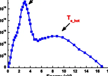
It has been discussed earlier that in low-temperature gas discharge plasmas Te is higher than the ions and neutral atoms temperatures (here denoted as Ti and Tg respectively). The electron energy distribution function (EEDF) in such a plasma discharge is non-
temperatures of the cold and hot electron populations, denoted as
ecold
T and
ehot
T respectively, are used as the representative and characteristic parameters for the respective populations. An example of such an EEDF from the measurements performed in a C-HiPIMS discharge in this works is presented in Figure 6.
Figure 6. An EEDF from a Ne-HiPIMS discharge of carbon, showing two distinct electron populations (cold and hot).
3.3 Ionization Processes
Electron temperature, Te, along with plasma density, ne, is the most influencing parameter in establishing how the plasma constituents interact with each other. In the plasma chemistry many mechanisms are working in parallel, which means that these two parameters are also important in determining dominating reactions through which the ionization of the sputtered material occurs. In a sputtering plasma, the most common ionizing mechanisms for sputtered material are, direct electron impact ionization, electron impact ionization of excited sputtered atoms and the ionization via the interaction with excited sputtering gas atoms (also called Penning ionization). These mechanisms are respectively represented as [26],
M0 + e- M+ + 2 e-, (3.4)
M* + e- M+ + 2 e-, (3.5)
M0 + G* M++ G0 + e-, (3.6)
where M and G respectively represent the sputtered and sputtering gas atoms.
Plasma discharges with high values of ne are dominated by electron impact ionization (processes in equations (3.4) and (3.5)) while the low ne discharges are dominated by Penning ionization (process in equation (3.6)) [29]. This is demonstrated in Figure 7 for the sputtering discharge of Al using Ar [29].
Figure 7. The process of ionization of sputtered Al at 36 mTorr of Ar gas pressure showing the region of dominance for electron impact and Penning ionization processes. (After J. Hopwood [29].)
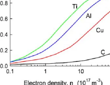
Figure 7 also demonstrates that a higher ionized fraction for the sputtered material is obtained with increased ne. This is a general trend for the sputtered material however, the absolute number of the ionized fraction varies with the material dependent cross sections for ionizing reactions. Metals are readily ionized with ne in the range of 1016 to 1019 m-3
Ei for C is 11.26 eV while for Al it is 5.98 eV). The dependence of the ionized fraction of the sputtered material on the plasma density is demonstrated in Figure 8 for various materials [26].
Figure 8. The ionized flux fraction dependence on plasma density for different materials. (After J.
Hopwood [26].)
The dependence of the degree of ionization of the sputtered material on Te and ne can also be understood by looking at the mean ionization length of a sputtered atom, which is the average distance the sputtered atom travels before it is ionized in a plasma discharge [26].
For the electron impaction ionization, the mean ionization length (here denoted as λmiz) of the sputtered atom can be expressed as [26],
mizvs kmizne, (3.7)
where vs is the velocity of the sputtered atom and kmizis the rate constant for electron impact ionization which is expressed as,
kmiz( )Te k0expE T0 e. (3.8)
The constants E0 and k0 are material dependent and they can be extracted from experiments or computer simulations [26, 30,31].
Equation (3.7) shows that an increase in both, Te and ne will result in the decrease in the λmiz which implies that the probability of the ionization of the sputtered material will increase. The exponential nature of kmiz (see equation (3.8)) suggests that the degree of ionization of the sputtered material is more sensitive to the changes in Te as compared to ne. As an example, the kmiz calculated using equation (3.8) for Te from 1 eV to 5 eV and a constant value of ne in a C-HiPIMS discharge is presented in Figure 9. It can be observed that a change of Te from 1 eV to 5 eV increases the kmiz by about 4 orders of magnitude.
Figure 9. kmizcalculated for a C-HiPIMS discharge operated with a mixture of Ar and Ne sputtering gases.
Increased values of Te are obtained with an increase in the Ne content of the sputtering gas whereas the Ar content of the mixture is constant.
4. Amorphous Carbon Growth
4.1 Introduction
Amorphous carbon (a-C) can be grown in variety of different forms; from pure disordered structure to crystalline as well as in hydrogenated (often denoted as a-C:H) and hydrogen-free forms [4,5]. The versatility of the material stems from its different hybridization states i.e. sp1, sp2 and sp3 bond configurations, which are depicted in Figure 10 [5]. In sp1 configuration, two of the four valence electrons of a carbon atom form σ (sigma) bonds directed along one plane (say x-plane) with its neighboring atoms, while the remaining two undergo a π (pi) bond formation in y and z planes. In sp2 bond coordination, three of the four valence electrons form σ bonds with neighboring atoms in the plane while the fourth electron forms a π bond, which is perpendicular to the σ bond plane. This means that the interlayer bonding is based on weaker π bonds. In sp3 configuration, all four valence electrons enter into σ bonds with neighboring atoms [5].
Since the σ bond is stronger as compared to π bond, the a-C film which are rich in sp3 bonds exhibit higher hardness than the one which is rich in sp2 bonds. In a-C:H, the sp3 bonds are contributed by C-H sp3 hybridization along with the C-C sp3 hybridization.
4.2 Different Forms of Amorphous Carbon
Possible forms of a-C are represented by the ternary phase diagram of a-C growth in Figure 11 [5]. The bottom right corner on this diagram defines the region where no C-C atomic bonds exist and therefore, no film formation is possible. Adjacent to that is the region of hydrocarbons. The bottom left corner is the region of sp2 rich carbon, examples of which are glassy carbon and pure graphite. Navigating along the left hand side, results in the bond fraction tailoring from sp2 to sp3. With films containing ideally no hydrogen, an increase in the sp3 bond fraction (about 50% or more) leads to the regime of diamond- like carbon (DLC). With further increase in the sp3 bonds (about 75% or more), the films are referred to as tetrahedral a-C (ta-C). It is also possible to reach to the middle of the triangle if the a-C films contain high amount of hydrogen and at the same time, exhibit a very high density. This regime is called ta-C:H [5].
Figure 11. Ternary phase diagram for a-C growth. (After J. Robertson [26].)
4.3 The Densification Model
As discussed in chapter 1, the sp3/sp2 bond ratio is vital for the functionality of hydrogen free a-C, which is the prime subject of this thesis. The sp3/sp2 bond ratio can be tailored by controlling the flux and energy of the depositing species. For the a-C growth, the dependence of energy and flux of the depositing species is described by the densification model [5] which is illustrated in Figure 12.
Figure 12. An schematic showing the densification model for the growth of a-C. (After J. Robertson [5].)
The densification model can be described as follows: Suppose that the depositing species possess a certain energy Einc and the atoms at the surface of the growing film are bounded with an energy Eb. Associated with these surface atoms, there is an energy which is termed as displacement energy, Ed, which is the energy required to displace an atom and form a vacancy-interstitial pair. The surface penetration threshold, Ep, is the combination of Ed and Eb, such that [5],
Ep = Ed + (-Eb). (4.1)
If Einc is lower than Ep, the incoming atoms reside on the surface in lower energy configuration, resulting in the outward growing sp2 layers. If Einc is greater than Ep, the incoming atoms penetrate through the surface and shallow implantation (also referred to as subplantation) occurs. This results in the increase in the vacancy-interstitial pairs thereby causing an increase in the local density in the subsurface region. Since the material is amorphous therefore, the incident atoms and the implanted atoms are the same;
a bond rearrangement from sp2 to sp3 occurs, which gives rise to an increase in the density of the films.
moderately higher incident energies as compared to Ep, the implantation occurs through the process of knock-on. At very high energies, thermal spike is caused. In the case of upper limit of energy for the knock-on process and in the region of thermal spike, there is an excess energy than what is required for the implantation. This excess energy appears in the form of heat (phonon) which causes a bond relaxation from sp3 to sp2 and as a consequence, the density of the film decreases to the initial level (before the implantation occurs). The Ep for carbon is about 35 eV while the optimum energy for the implantation is found to be about 100 eV. Typical energy range of interest is between 10 – 1000 eV.
With this energy range, initially a transition from sp2 dominated growth to sp3 dominated growth occurs, and after the optimum is reached, the relaxation occurs. Figure 13 shows the experimental verification of the densification model including the processes of densification and relaxation [32].
Figure 13. An experimental verification of the densification model of a-C growth showing the dependence of the densification and relaxation on the energy of the depositing ions. (After Mckenzie [32].)
From the discussion of the densification model, it can be understood that the growth of denser and sp3 rich a-C requires an energetic depositing flux. It is also important that the energy of the depositing flux can be controlled. This will be much easier if a large
fraction of the depositing flux is ionized. Highly ionized depositing fluxes are provided by the IPVD methods therefore, it is instructive to discuss the role of IPVD methods for the growth of a-C films.
5. Amorphous Carbon Growth and Ionized PVD
Among the IPVD methods, the state of the art approaches for the growth of denser and sp3 rich a-C include FCVA and PLD. HiPIMS has successfully demonstrated its potential as an IPVD method for most commonly used metals (such as Cu, Ti, Ta). It is therefore also important to discuss the role of HiPIMS for the growth of a-C. In the following sections, a brief account of each of these methods will be presented in connection to the growth of a-C.
5.1 Filtered Cathodic Vacuum Arc
Cathodic vacuum arc discharges are the forefront of ion-assisted energetic deposition. In a cathodic arc discharge, the source material is vaporized by using a high-current, low- voltage arc at the target (cathode) surface [17]. The arc forms cathode spots which are non-stationary locations of current density in the range of 106 – 108 Acm-2. The associated power density is in the order of 107 Wcm-2. Such a high current and power densities result in the phase transformation of the target material — from solid to highly ionized plasma. The plasma thus generated expands into vacuum ambient, with its constituting ions possessing a velocity in the order of 1 – 2x10⁴ ms-1, resulting in the ion energies between 20 eV to 200 eV while the ionized fraction of the source material can reach up to 100% [17]. Creation of highly ionized depositing fluxes in such a discharge is also accompanied by the ejection of droplets and debris particles from the cathode
macroparticles out before they reach to the substrate. This filtration leads to the modified form of cathodic arc deposition, which is known as filtered cathodic vacuum arc (FCVA) [33]. FCVA discharges can be operated in DC as well as in pulsed mode. In the DC mode, the current is in the range of 50 – 150 A while the pulsed discharges provide higher current in the order of about 1000A [33, 34].
Plasma properties in FCVA such as ne in the order of 1020 – 1021 m-3, Te up to 10 eV and the highly ionized (up to 100%) depositing flux — having ion energies as high as 200 eV
— make it a suitable choice for the ion-assisted film growth especially for the synthesis of sp3 rich a-C [10]. FCVA has been extensively employed for the synthesis of high density and sp3 rich a-C. In such a case, C ion energies of about 20 – 30 eV in DC arc discharges while a wider energy range of 20 – 140 eV in pulsed arc discharges have been reported [10]. The energetic depositing flux of C has been shown to provide a-C films with mass density reaching up to 3.2 gcm-3, sp3 fraction of about 88% and the hardness of about 90 GPa [10]. The grown a-C film properties from FCVA are promising however, the drawbacks with this technique such as lack of lateral film uniformity, reduction of the deposition rate due to macroparticle filtration as well as difficulty to produce defect-free coatings (due to the fact that 100% macroparticle filtration can not be achieved) are the major concerns over its implementation at industrial scale especially for the production of high quality and cost-effective a-C coatings for optical and electronic applications.
5.2 Pulsed Laser Deposition
In PLD, the source material is evaporated using laser irradiation in the form of small (15 – 30 ns) pulses. The process of evaporation is accompanied by a luminous intensity plasma cloud hurled over and traveling normal to the target, which is also called ‘plume’.
The plume contains high-energy (substantially higher than thermal energies) neutrals and ionized atoms as well as clusters of the target material [16, 35]. Commonly used lasers for the process of pulsed laser deposition are 193 nm ArF and 248 nm KrF excimer lasers.
In this method, the power densities at the target surface due to focused laser beams can reach in the order of 50 – 500 MWcm-2 [35]. For the case of a-C growth, the energies of the evaporated material and the plasma density in the plume meet the energetic
deposition conditions, which are required for the synthesis of sp3 rich a-C. The densities of a-C grown with PLD as high as about 3 gcm-3, with hardness of the films reaching 100 GPa have been reported [5,16,35] and therefore, the technique is regarded as a viable IPVD method for the synthesis of DLC and ta-C. However, there are drawbacks that are inherent to the method such as, source material cluster evaporation, lower deposition rate, costly setup, lack of lateral uniformity of the grown films as well as difficulty in making large area depositions [16]. These constraints limit the up-scaling of the technique and hence the irrelevance to the industrial setup results.
5.3 High Power Impulse Magnetron Sputtering
As it was discussed in chapter 2, a HiPIMS discharge is usually operated at the peak target power densities in the order of kWcm-2, which results in ne in the order of 1018 to 1019 m-3 [15]. The energy distribution of the sputtered material in a HiPIMS discharge follows a Thomson-like (Thomson distribution with high-energy tail) distribution. At low operating pressures, the high-energy tail may extend from 10 – 100 eV for the case of metals (such as for Ti) [18,19]. However, the low-energy thermalized ions still dominate the energy distribution, giving the average ion energy slightly higher than that of DCMS while the Te is quite similar (few eV) to what is obtained from DCMS discharges [15].
This implies that the energetic deposition conditions do not exist unless the energy of the depositing flux is manipulated by some external means such as by applying a substrate bias potential. However, in contrast to DCMS, this is possible with HiPIMS as the ion-to- neutral ratio, due to 2 to 3 orders of magnitude higher ne, is very high (up to 90% for Ti) [19].
The main reason for a highly ionized metal depositing flux achieved in the case of a HiPIMS discharge is the low Ei values of metals ( which are typically in the range of 6 to 8 eV for commonly used metals). Non-metals such as carbon, on the other hand, have substantially higher Ei values (such as 11.26 eV for C) and therefore, they are difficult to
C despite the fact that the plasma density is high. Highly ionized depositing fluxes of sputtered carbon are therefore not achieved, which are essential for the synthesis of denser and sp3 rich a-C. The best results reported so far give the film density of about 2.2 gcm-3 and sp3 bond fraction of about 45% using HiPIMS [21].
The state-of-the art of a-C growth emphasizes on the fact that in terms of film density and sp3 bond fraction, the best results are obtained with FCVA and PLD. The quality of the coatings, the simplicity of the method and its cost effectiveness for large scale production as well as upscalability are desired for an industrial process and FCVA and PLD lack in these areas. HiPIMS, being a magnetron sputtering based technique, has a potential to demonstrate these features and therefore it can provide an industrially relevant process for a-C growth. In terms of film properties such as mass density and hardness, HiPIMS is well behind FCVA and PLD. The conventional HiPIMS process therefore requires modifications in order to produce a-C coatings with properties comparable to FCVA and PLD.
6. Research Strategy and Experimental Details
6.1 Research Strategy
It was discussed in the previous chapter that the difficulty encountered with HiPIMS in creating highly ionized C fluxes is mainly due to low electron impact ionization cross section for C and insufficient electron temperature, Te. It should be noted that the plasma density, ne, in C-HiPIMS discharge, comparable to that of metal-HiPIMS discharge (of the order of 1018 m-3, as determined in this research) can be obtained. Thus, the only way to further increase the degree of C ionization in a HiPIMS discharge is by increasing Teas show in equation (3.7). The strategy adopted in this research is based on increasing the ionization of C by increasing Tein a C-HiPIMS discharge. The Teof a plasma discharge is set by the ionization energy, Ei, of the sputtering gas. This implies that a plasma discharge created using a high Ei gas should contain energetic electrons. Conventional C-HiPIMS discharges are operated using Ar (Ei value of 15.6 eV) as sputtering gas. This means that higher Tecan be obtained if Ne or He (having Eivalues of 21.56 eV and 24.58 eV respectively) is used, instead of Ar. In this work, Ne was used for C sputtering using a HiPIMS process at 2 Pa and 4.66 Pa. A difficulty encountered with Ne was its ignition at lower operating pressures, such as at 2 Pa, due to its high Eivalue. This difficulty can be overcome by means of pre-igniting the discharge. In this work, a new method for the pre- ignition of a discharge is introduced, which uses a mixture of a low Ei gas (which is


![Figure 11. Ternary phase diagram for a-C growth. (After J. Robertson [26].)](https://thumb-eu.123doks.com/thumbv2/5dokorg/5455790.141534/34.892.252.643.563.812/figure-ternary-phase-diagram-c-growth-j-robertson.webp)
