FACULTY OF ENGINEERING AND SUSTAINABLE DEVELOPMENT
.
Designing and measurement of routing
module for transceiver system at 3.125GHz
Nauman Afzal
Ramakrishna Udata
January 2014
Master’s Thesis in Electronics
Master’s Program in Electronics/Telecommunications
Examiner: Jose Chilo
i
Abstract
This report intends to impart a good understanding of routing modules used in modern transceiver systems. The radar system at RadarBolaget AB needed to have a good routing module for its newly designed transceiver antenna. In this report, studies have been done related to two majorly used routing modules in modern electronics industry; Microwave Circulator and RF/Microwave Switch. First off, different characteristics of routing modules are discussed. After having discussed important design parameters, practical design considerations for two routing modules are presented in a profound way. Theoretical knowledge for both of these two devices is presented in the beginning, followed by their practical designs using standard simulation software like HFSS and ADS. The report concludes its findings in a way that at the end of this report, reader becomes acquainted with ample information to be able to choose the best option available among all of the discussed designs. An FET RF Switch is chosen at the end of this project to be used for transceiver system which should be able to satisfy specifications specified by RadarBolaget AB. This project was carried out by two students of Master Program in Electronics/Telecommunications at Högskolan i Gävle in collaboration with RadarBolaget AB, Gävle, Sweden.
ii
Acknowledgement
The authors would like to express their cordial thanks to their Thesis supervisor Daniel Andersson for his consistent support and guidance throughout the project. Thanks are extended to our additional supervisor Patrik Ottoson, CEO RadarBolaget, for provision of an office cabin and additional equipment which really helped us in carrying out this research work. Our courteous appreciation goes to two of our Ph.D. student fellows, Efrain Zenteno and Shoaib Amin, as without their friendly advice and suggestions on the matter, this would not have accomplished. At the end, our family members and all friends who helped along the way, deserve our appreciation.
Nauman Afzal Ramakrishna Udata
iii
List of Acronyms
Acronym Abbreviation
AC Alternate Current
ADS Advanced Design System
BW Band Width
DC Direct Current
FMR Ferro Magnetic Resonance
FET Field Effect Transistor
HFSS High Frequency Structural Simulator
IEEE Institution of Electrical and Electronics Engineers
𝐼𝑃
3Third Order Intercept Point
𝐼𝐼𝑃
3Input Third Order Intercept Point
JFET Junction Field Effect Transistor
MOSFET Metal Oxide Semiconductor Field Effect Transistor
𝑂𝐼𝑃
3Output Third Order Intercept Point
RF Radio Frequency
RM Routing Module
𝑅
𝑥Receiver
SPST Single Pole Single Through
SPDT Single Pole Double Through
𝑇
𝑥Transmitter
TL Transmission Line
TEMW Transverse Electro Magnetic Wave
UWB Ultra Wide Band
VSWR Voltage Standing wave ratio
YIG Yttrium Iron Garnet
iv
Table of Contents
Abstract ... i
Acknowledgement ... ii
List of Acronyms ... iii
1. Introduction ... 1
1.1 Background ... 1
1.2 Goal ... 2
1.3 Outline... 2
2. Theory ... 3
2.1 Important Design Parameters ... 3
2.1.1 Frequency of operation and bandwidth ... 3
2.1.2 Insertion loss ... 3
2.1.3 Isolation ... 3
2.1.4 Return loss and VSWR ... 4
2.1.5 Reflective or absorptive ... 4
2.1.6 Distortion ... 4
2.1.7 Number of throws ... 4
2.2 Microwave circulator ... 5
2.2.1 Working principle ... 5
2.2.2 Microwave circulator Design principle ... 10
2.3 Microwave/RF Switch ... 13
2.3.1 PIN Diode Switch ... 14
2.3.2 Field-Effect Transistor Switch ... 16
3. Simulations and Results ... 20
3.1 Simulations for Microwave Circulator ... 21
3.1.1 Experimental Design of Microwave circulator ... 21
3.2 Simulations for PIN diode Switch ... 30
3.2.1 Series PIN SPDT Switch... 30
3.2.2 Shunt PIN SPDT Switch ... 33
3.2.3 Series-shunt PIN SPDT Switch ... 35
3.2.4 Very High Isolation Switch ... 37
3.3 Simulations for FET Switch ... 39
4. Measurements ... 51
5. Discussion and Conclusion ... 54
v 7. Appendix ... A 7.1 Types of transmission lines ... A 7.1.1 Strip line ... A 7.1.2 Micro-strip line ... A 7.1.3 Single ended line and differential line signalling systems ... B 7.1.4 Single ended line signalling system ... B 7.1.5 Differential line signalling system ... C 7.1.6 The circulation approximation ... C 7.1.7 The 3D- view of the circulator & its Electric field distribution ... E
1
1. Introduction
1.1 Background
With the evident upsurge in the technological development, wireless communication has found its way in many aspects of today’s life. The process communication needs some kind of information to be delivered from one point to another. The set of information/data is transmitted through a device called
transmitter, travels through a portion of the electromagnetic (EM) spectrum via microwave links or
transmission lines, and received at the other end by an electronic device called receiver. Transmitter and receiver both have been effectively used for their specific tasks for last many decades, but when these two devices are combined together to be used as one single module, performing the dual function, it is referred to as transceiver. Transceiver design varies according to the specific requirement, but one basic transceiver design is presented in Figure 1.
Low Noise Amplifier
Maximum Gain Amplifier
Local Oscillator Local Oscillator Routing module Antenna Towards Receiver From Transmitter
FIGURE 1. BASIC TRANSCEIVER DIAGRAM [1]
In Figure 1, there is a component labelled, “Routing module” (it can also be called as switching device, but in this report it will be referred to as routing module (RM)). This very component is the pivotal component in any transceiver system, as would it not be there, transmitter and receiver can’t work together as one single device. Function of this routing module is to route the signal efficiently among transmitter, antenna and receiver, i.e. during transmission, it should only allow the signal to be transferred from transmitter to antenna and should block the signal from going towards the receiver. Similarly, when a signal is received through antenna, this routing module is responsible to direct the signal towards receiver and obstructing the signal from entering the transmitter. So, any device performing this particular function of transmission of power to a particular port while stopping the power being transferred to the other or rest of the ports, can be called as a routing module. There are
2 two major components in today’s electronic industry that are used as this routing module; Microwave
circulator and RF/Microwave switch.
1.2 Goal
The main goal of this thesis report is to select one good routing module for a transceiver system used at RadarBolaget AB Gävle, Sweden. In the first stage, two mostly used routing modules in modern transceiver systems will be designed according to the specifications mentioned in Table 1. And in the second stage, best routing module will be chosen on the basis of obtained results. The chosen routing module will either be manufactured or the client (RadarBolaget) may decide to buy the commercial one which should be complying with the specifications. Specifications that need to be fulfilled by the routing module to be designed are as follow.
Operating Frequency 𝒇𝒐 3.125GHz
Bandwidth 50% of 𝑓𝑜
Insertion loss ≥ -1.5dB
Isolation ≤ -50dB
Return loss ≤ -15dB
TABLE 1. ROUTING MODULE SPECIFICATIONS
1.3 Outline
This thesis report deals with the study of routing modules used in modern electronics industry. Two most important routing modules; Microwave circulator and RF/Microwave switch are presented in this report in a profound way. In Chapter 2, theoretical concepts important to fully understand the working principle of these two routing modules are discussed. Then in Chapter 3, these theoretical concepts are put into practical design considerations using standard simulation software like HFSS and ADS. Results are also presented in tabular form which enables the reader to compare the results easily. On the basis of results obtained and comparing commercially available routing modules, one suitable routing module is selected according to the requirements/specifications imposed by the client (RadarBolaget AB). Measurements done with the selected routing module are presented in Chapter 4. Conclusive statement about the report is presented in Chapter 5.
3
2. Theory
2.1 Important Design Parameters
This report deals with the design procedure, result analysis and comparison of two routing modules, but before going into the design details, let’s get familiar with some of the important performance parameters which are generally taken into account while designing these routing modules.
2.1.1 Frequency of operation and bandwidth
The desired frequency of operation and the allowed bandwidth is the foremost design consideration any designer will have to deal with. With the rapid growth of wireless applications and systems, frequency spectrum has found its limitations in terms of available frequency bands. In this case, broadband devices have definitely an upper hand over narrow-band devices. Use of broadband devices eliminates the cost of up gradation in case of the requirement for the system to be used for higher frequency range.
2.1.2 Insertion loss
Insertion loss refers to the power loss of the transmitted signal. Insertion loss is the measure of power loss and signal attenuation and it varies with frequency [2]. The transmitted signal power loss, adversely affects the overall performance of the system. Additional power is then required to compensate for the power loss which itself becomes a limitation because of the limited power handling capability of the device [3]. Power loss is suffered by the transmitted signal due to two factors.
Because of the presence of resistive components like parasitic capacitance, inductance and resistance in the device signal is transmitted through.
And because of high VSWR created due to mismatch between the ports or transmission lines involved in the design.
2.1.3 Isolation
Isolation in simple words can be defined as ‘very high transmission loss’. It is expressed in decibel (dB). As discussed in ‘introduction’, routing module is supposed to deliver power to one of its ports and block the power from entering the other port. The port where signal is supposed to enter to, is referred to as on-port and port which was blocked for the incoming signal, is referred to as off-port. By this, isolation can be defined as, “the ratio of power level in the off-port to the power level in the on-port”. In other words, isolation is the suppression of the signal in excess of the insertion loss at the off-port [3]. Isolation indicates the ability of the device to prevent stray signals leaking into the off-off-port. Leaked signal entering the off-port results in reflections and ultimately results in poor performance. Higher the isolation level, better will be the performance. Isolation becomes even more critical consideration in devices which involves the signal entering and leaving more than one port.
4
2.1.4 Return loss and VSWR
Voltage Standing Wave Ratio ‘VSWR’ is the degree of reflected signals in a device and when it is expressed in dB, it is referred to as ‘Return loss’. Reflections occur in any device due to impedance mismatch between device components or the device itself with other devices. At higher frequencies, any component’s dimensions along with its physical parameters are responsible in determining impedance match or mismatch with other device components. Increased bounced-back signals, resulting from poor matching between the components, reduce the power transfer. Higher values of return loss indicates that reflected signal suffer much obstruction on its way back towards the signal source, so, higher the return loss, better the matching and ultimately efficient the performance.
2.1.5 Reflective or absorptive
Another important design parameter of the routing module is being ‘reflective or absorptive’. If the routing module is reflective, the RF signal is reflected back towards the signal source from the off-port. Reflective designs are relatively simpler and cost economical. On the other hand, the off-port is required to be terminated with a matched termination in order to make the design absorptive. Generally, absorptive designs are bit sophisticated and of course expensive. Microwave circulator design presented in this report is absorptive while RF switch designs are reflective.
2.1.6 Distortion
Distortion due to intermodulation products and harmonics is another key design factor that is taken into account. Harmonics are integral multiples of the fundamental frequency the device is operated at. At these harmonic frequencies, spurious output signals are generated which tend to make the device/system non-linear. Similarly, non-linearity arises by the mixing of harmonics of two or more frequencies. Broadband systems are more prone to be affected by distortion due to harmonics and intermodulation product. Third-order intermodulation product is closest to the fundamental frequency to be easily filtered [4].
2.1.7 Number of throws
Number of throws of the routing module is specified by the topology of the network it is used in. Generally, three-port device for both switch and circulator is used to be able to use them in transceiver systems with one port attached to transmitter, another port to antenna and the third port to the receiver. If routing module is used for applications where diversity technique using multiple antennas is implemented, then routing module needs to have more than three ports according to the requirement. Similarly, in order to increase isolation, microwave circulators are designed sometimes to have four ports with one extra port terminated to reduce reflections. But, on the other hand, the module becomes more prone to losses (insertion loss) as number of throws is increased [2]. So, a balance between isolation and insertion loss must be consider while deciding the number of throws.
5 After having discussed important design parameters, let’s now have a look at the theoretical working principle of the two important routing modules; Microwave circulator and RF/Microwave switch. Next sections in this report, deals with the study of these two routing modules. This theoretical knowledge will be applied in terms of simulations to be able to verify the behaviour of these devices in real life.
2.2 Microwave circulator
Microwave circulator is a passive device which has been used in microwave circuits for decades. The Y-junction microwave circulator is typically having 3 ports (input port, output port and decoupled port). The main reason for using this junction circulator is energy supervision. Circulator allows the maximum power transfer from one port to another port in a way that the power flows from input port to output port and 3rd port will be isolated. It is like the power enters at port 1 is fully transmitted to port 2, power enters at port 2 is completely transmitted to port 3 and power enters at port 3 is completely transmitted to port 1. At the same time the circulation can take place in reverse direction too. That is, the power enters at port 1 is fully transmitted to port 3 and port 2 will be isolated, the power enters at port 3 is completely transmitted to port 2 and port 1 will be isolated and so on. Such device is versatile and it has many applications, it can be used as a switch and like a duplexer in communications and radar systems.
2.2.1 Working principle
In the Microwave circulator theory part, a brief explanation about the related electromagnetic fields is discussed with the help of Maxwell equations. A brief explanation is presented about the Ferromagnetic materials which includes an active magnetic component’s (YIG) structure, which is necessary in the design and operation of a microwave circulator. A brief explanation is included about how the circulation exactly takes place in a Y-junction circulator when external magnetic field is applied at various stages.
2.2.1.1
Electromagnetic Fields Study
Maxwell equations: The working of electric and magnetic fields are very well described by using standard Maxwell equations [5], and is given as equation (1) below
∇ × E⃗⃗ = −𝛿B⃗⃗ 𝛿𝑡 (1𝑎) ∇ × 𝐻⃗⃗ = 𝛿𝐷⃗⃗ 𝛿𝑡 + 𝐽 (1𝑏) ∇. 𝐷⃗⃗ = 𝜌 (1𝑐) ∇. 𝐵⃗ = 0 (1𝑑)
6 Where
E is the electric field intensity in V/m. H is the magnetic field intensity in A/m. D is the dielectric flux density in C/𝑚2. B is the magnetic flux density in Wb/𝑚2. J is the electric current density in A/𝑚2. 𝜌 is the electric charge density in C/𝑚3.
Now the relation among these quantities in free space or in vacuum is given as B
⃗⃗ = μ0H⃗⃗ (2)
𝐷⃗⃗ = 𝜖0𝐸⃗ (3)
Where
𝜇0 is the permeability in free space and its value is 1.256×10⁻⁶ H/m
𝜖0 is the permittivity in free space and its value is 8.854×10⁻¹² F/m
In anisotropic magnetic materials (ferrites), equation (2) and (3) can be visualized in terms of vector form given as [ 𝐷𝑥 𝐷𝑦 𝐷𝑧 ] = [ 𝜖𝑥𝑥 𝜖𝑥𝑦 𝜖𝑥𝑧 𝜖𝑦𝑥 𝜖𝑦𝑦 𝜖𝑦𝑧 𝜖𝑧𝑥 𝜖𝑧𝑦 𝜖𝑧𝑧 ] [ 𝐸𝑥 𝐸𝑦 𝐸𝑧 ] (4) [ 𝐵𝑥 𝐵𝑦 𝐵𝑧 ] = [ 𝜇𝑥𝑥 𝜇𝑥𝑦 𝜇𝑥𝑧 𝜇𝑦𝑥 𝜇𝑦𝑦 𝜇𝑦𝑧 𝜇𝑧𝑥 𝜇𝑧𝑦 𝜇𝑧𝑧 ] [ 𝐻𝑥 𝐻𝑦 𝐻𝑧 ] (5)
Where μ is the permeability tensor given in equation (6)
μ = 𝜇0(1 + 𝜒𝑚) (6𝑎) μ = 𝜇0(1 + 𝜔𝑚𝜔0 𝜔02− 𝜔2 ) (6𝑏)
2.2.1.2
Ferromagnetic materials
7 These are called ferrites and they typically have the elements with two or more sub lattices. So the effect between the ions in different sub lattices gives push to opposing magnetic moments which are unequal. Hence a net magnetization exists in ferrites. There are 3 types of ferrites available and they are called garnets, spinel ferrite and hexagonal ferrite. Each one indicates different crystal structures. Garnets are taken into account for the scope of this project and will focus on Yttrium Iron Garnet (𝑌3𝐹𝑒5𝑂12). This
material can work as an active element in the design of circulator which has properties similar to other ferrite materials [6].
2.2.1.3
YIG structure
The YIG lattice structure is a cubic, with three sub lattices. The 1st sub lattice is tetrahedral (d-site), 2nd one is octahedral (a-site) and the 3rd one is dodecahedral sites (c-site). The 𝐹𝑒3+ ions placed on tetrahedral and octahedral sites are surrounded by 𝑂2− ions. The 𝑌3+ ions placed on the dodecahedral
sites and surrounded by 𝑂2−ions. The 𝑂2− ions can work as an intermediate which makes the interaction between the tetrahedral and octahedral sites possible. The 𝐹𝑒3+ ions at tetrahedral site has a magnetic moment, which is anti-parallel to both 𝐹𝑒3+ ions in the octahedral sites and 𝑌3+ ions in the
dodecahedral sites. All these anti parallel moments are not going to cancel exactly with the parallel moments, so a net magnetization will be there in YIG. YIG has a saturated magnetization at room temperature and it is around 1750G [6].
FIGURE 2 YIG STRUCTURE
From the electromagnetic field theory, any magnetic material can be used to obtain the circulation. But in this project case, YIG is used, because it acts like most of the ferrite materials and it is a good insulator. It optimizes all the unwanted eddy current losses and they can be reduced to a better level [7]. In the next section of the theory, a brief discussion about the working principle of the circulator with important magnetic phenomenon is presented.
8
2.2.1.4
Characteristics of ferrite
The characteristics of ferrite completely depend on the dipole of the magnet, i.e. the electron spin [8]. The spin of the electron can be seen in the Figure 3 and its magnetic dipole momentum is given in equation (7)
FIGURE 3. ELECTRON SPIN IN THE MAGNETIC FIELD
The momentum is
𝑚 = 𝑞ℎ
2𝑚𝑒
(7) Where ‘h’ is the planks constant and its value is 6.626× 10⁻³⁴𝑚2𝑘𝑔/𝑠.
The spin angular moment of the electron is given as
𝑠 =ℎ
2 (8)
If an external magnetic field is applied, then the ferrite will be magnetized and the permeability tensor will be expressed as following equation (9)
𝜇 = ( 𝜇0 0 0 0 𝜇 𝑗𝑘 0 −𝑗𝑘 𝜇 ) (𝑥 − 𝑏𝑖𝑎𝑠𝑒𝑑) (9𝑎) 𝜇 = ( 𝜇 0 −𝑗𝑘 0 𝜇0 0 𝑗𝑘 0 𝜇 ) (𝑦 − 𝑏𝑖𝑎𝑠𝑒𝑑) (9𝑏)
9 𝜇 = ( 𝜇 𝑗𝑘 0 −𝑗𝑘 𝜇 0 0 0 𝜇0 ) (𝑧 − 𝑏𝑖𝑎𝑠𝑒𝑑) (9𝑐)
2.2.1.5
Ferromagnetic resonance (FMR)
From the equation (6b) if 𝜔 = 𝜔0, at this particular frequency, the permeability tensor can have a
singularity, this is the point where the ferromagnetic resonance (FMR) occurs. Maximum energy transfers occurs, when the driving frequency (𝜔) of electromagnetic wave reaches to the internal field frequency (𝜔0) of the ferrite. Applying an electromagnetic wave at resonance frequency gives more
losses because the ferrite wouldn’t have the enough saturation magnetization at resonance point. [8].
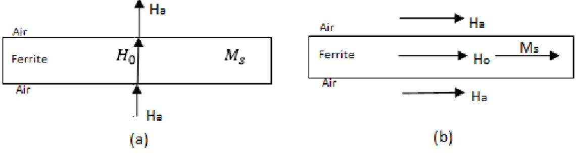
FIGURE 4. APPLIED MAGNETIC FIELD (A) PERPENDICULAR (B) PARALLEL TO FERRITE FIELD
The static magnetic field is applied here and it is perpendicular to the internal field and parallel to the internal field. Magnetic field applied perpendicular to the internal field is used in the YIG disk biasing for the good circulation, i.e. maximum power transmission.
2.2.1.6
Below and above resonance frequency regions
Since it is undesirable to operate the circulator at FMR frequency, the operation of the circulator will be checked at below resonance mode and above resonance mode frequencies.
Lower magnetic field biasing (𝐻𝑜) is required in the below resonance mode of operation but this is not enough to saturate the ferrite. It may result bad circulation.
i.e. 𝜔0< 𝜔
𝜔0= 𝜇0𝛾𝐻0
At the same time, higher magnetic field biasing (𝐻𝑜) is required in the above resonance mode of operation. The ferrite can saturate in excess, so the losses will be decreased and gives good circulation.
i.e. 𝜔0> 𝜔
10 The selection between these two modes depends on the magnetic loss mechanism. Hysteresis loss can be decreased by applying the higher static magnetic field, so the ferrite will be saturated in excess. The below resonance mode is eliminated because the lower field loss region can merge with the FMR region when higher magnetic field is applied so gives bad circulation. So, the circulator has been designed at above resonance region to overcome the hysteresis losses and also the YIG can be saturated in excess with higher magnetic field biasing.
2.2.2 Microwave circulator Design principle
The junction microwave circulator is the most commonly used circulator and its pictorial view is shown in Figure 5. The micro strip line conductors are covered by the two ferrite disks. These conductors are separated at 120° intervals, will form the 3 ports of the circulator. An external magnetic field is applied normal to the ferrite disks.
FIGURE 5. MICRO-STRIP CIRCULATOR
In the circulator operation, the ferrite disk has a single resonant mode Cos (∅) or Sin (∅) when there is no external magnetic bias field applied. When the ferrite is biased by the external magnetic field, then the operation will be divided into two resonant modes – above and below resonant modes. According to the operating frequency of the circulator and magnetic losses occurring in ferrite, the mode of operation will be selected. Here the centre conductor is anti-symmetric, so that the solution for one of those ferrites can be considered, since the applied magnetic field is same on above and below the ferrite disks [8], [9].
2.2.2.1
Circulation existing principle
There are total 3 cases to check the standing wave pattern that exist during circulation, a) When the ferrite disk is not magnetized
b) Ferrite disk magnetized below the resonance c) Ferrite disk magnetized above the resonance
11
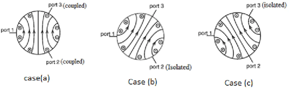
FIGURE 6. STANDING WAVE PATTERNS; THREE CASES
Case a
According to the Fay and Comstock explanation [10], when there is no external magnetic field applied to the ferrite disk, the power entering at one port will split into two equal divisions and transferred to the other two ports. This is shown in Figure 6a, Here the wave enters at port 1 will be divided into two rotating waves with the same propagation speed, one wave will rotate clock wise and reach to port 3 and the other will rotate anti-clock wise and reach to port 2. These two ports will be coupled.
Case b
When an external permanent magnetic field is applied in the direction normal to the ferrite disk, then the propagation speed of the standing wave will not be same any more. If there is certain amount of rise in the applied magnetic field, then the standing wave start rotating in the clockwise direction and the angle of rotation must be 30°, then the device is circular. That means all power will be transferred from port 1 to the port 3 and port 2 will be decoupled. This is shown in Figure 6b. In this case, the applied static magnetic field is lower than the resonance of the ferrite. So, it is called below resonance mode.
Case c
Circulation can be reversed by interchanging the isolated port with the through port. For example, in Figure 6c port 1 is excited and port 3 is designed to have null response. If even more static magnetic field is applied, then the standing wave will start rotating in 30° anti-clockwise and port 3 will be decoupled and all the power will be transferred from port 1 to port 2. In this case, the applied static magnetic field is higher than the ferrite resonance. So this mode is called above resonance.
2.2.2.2
Ideal circulation condition
The ideal circulation condition will be proved by using S-parameters. S-parameters explains about the properties of the circulator [11]. The basic scattering matrix for a 3 port circulator is given as
12 [𝑆] = [ 𝑆11 𝑆12 𝑆13 𝑆21 𝑆22 𝑆23 𝑆31 𝑆32 𝑆33 ] (10)
Basically, a circulator is a lossless device and this condition exists when 𝑆∗𝑆 = 1 (11)
The symbol ‘*’ represents the complex conjugation. This is true when it is completely matched and there is no mismatch at the ports.
𝑖. 𝑒 𝑆11= 0, 𝑆22 = 0, 𝑆33= 0 (12)
Now from equation (11) → [
0 𝑆12 𝑆13 𝑆21 0 𝑆23 𝑆31 𝑆32 0 ] [ 0 𝑆∗21 𝑆∗31 𝑆∗12 0 𝑆∗32 𝑆∗13 𝑆∗23 0 ] = 1 |𝑆12|2+ |𝑆 13|2= 1 (13𝑎) |𝑆21|2+ |𝑆23|2= 1 (13𝑏) |𝑆31|2+ |𝑆 32|2= 1 (13𝑐) 26(𝑎) → 𝑆∗12𝑆13= 0 (13𝑑) 26(𝑏) → 𝑆∗21𝑆23= 0 (13𝑒) 26(𝑐) → 𝑆∗31𝑆32 = 0 (13𝑓)
From the above 6 equations (from 13a to 13f), it can be clearly noticed that
𝑆12= 𝑆23= 𝑆31= 1 𝑎𝑛𝑑 𝑆13= 𝑆21= 𝑆32= 0 (14)
Or
𝑆12 = 𝑆23= 𝑆31= 0 𝑎𝑛𝑑 𝑆13= 𝑆21= 𝑆32= 1 (15)
According to the equations (14) and (15), one can confirm, that this device is totally a lossless device and fully matched at its ports, and also this device is a non-reciprocal (𝑆𝑝𝑞≠ 𝑆𝑞𝑝) device.
Now for an ideal circulator, with lossless and fully matched condition, according to equation (14), the scattering matrix is given as
13 [𝑆] = [ 0 1 0 0 0 1 1 0 0 ] (16) 𝑝𝑜𝑤𝑒𝑟 𝑡𝑟𝑎𝑛𝑠𝑓𝑒𝑟 𝑓𝑟𝑜𝑚 𝑝𝑜𝑟𝑡 1 → 𝑝𝑜𝑟𝑡 3, 𝑝𝑜𝑟𝑡 3 → 𝑝𝑜𝑟𝑡 2, 𝑝𝑜𝑟𝑡 2 → 𝑝𝑜𝑟𝑡 1 (𝑎𝑛𝑡𝑖 − 𝑐𝑙𝑜𝑐𝑘𝑤𝑖𝑠𝑒) . Now for an ideal circulator with lossless and fully matched condition, according to equation (15), the scattering matrix is given as
[𝑆] = [ 0 0 1 1 0 0 0 1 0 ] (17) i.e. 𝑝𝑜𝑤𝑒𝑟 𝑡𝑟𝑎𝑛𝑠𝑓𝑒𝑟 𝑓𝑟𝑜𝑚 𝑝𝑜𝑟𝑡 1 → 𝑝𝑜𝑟𝑡 2, 𝑝𝑜𝑟𝑡 2 → 𝑝𝑜𝑟𝑡 3, 𝑝𝑜𝑟𝑡 3 𝑝𝑜𝑟𝑡 1 (𝑐𝑙𝑜𝑐𝑘𝑤𝑖𝑠𝑒).
Hence, for the lossless and non-reciprocal condition, one can use a low loss ferrite, since the permeability tensor is anti-symmetric, i.e. the magnetic property is greatly directional dependent.
2.3 Microwave/RF Switch
RF and microwave switches are used extensively in transceiver systems for effective routing of the RF signal. RF switch is an active device and needs external biasing to put it into operation. There are two main types of RF switches.
Electro-mechanical switch Solid-state switch
Electro-mechanical switch is the one, in which mechanical components such as relays are operated by applying electric current to allow them to route the signal in a particular direction. Electro-mechanical switch has wide band operation (DC to 40GHz or higher) with remarkable insertion loss and isolation performance [2]. On the other hand, these switches have limited lifetime because of limited life of mechanical components used in them. Moreover, due to their inability to be used as surface mount chip designs, there is another type of switch known as solid-state switch used in modern transceiver systems. Solid-state switch is the one, which consists of solid-state components. Solid-state components are those which conduct current by the flow of electrons through solid semiconductor materials and no mechanical component, like relay, is required to control the amount of current. These switches have several advantages over their electro-mechanical counterparts. First off, solid-state switches can be used as surface mount ICs which makes them extremely smaller in size. Their switching speed is quite faster than electro-mechanical switches due to the fact, that current switching takes place because of alteration in internal structure of semiconductor material rather than the physical movement of the mechanical components. There are two types of solid-state switches; PIN diode switches and Filed-effect Transistor switches.
14
2.3.1 PIN Diode Switch
2.3.1.1
PIN Diode Fundamentals
The basic geometry of PIN diode is in such a way, that a high resistivity intrinsic “I” region is sandwiched between highly doped P-type and highly doped N-type materials as shown in Figure 7 [12]. PIN diodes act as a resistor, whose resistance can be varied with the applied voltage at RF and microwave frequencies [13]. In PIN diodes, the epitaxial layer (I-region) is designed to be quite thick. Small physical size of PIN diode make it a suitable candidate to be used in applications that require fast switching, miniature size and low package capacitance. According to the polarity of the applied voltage, PIN diode is either forward bias or reverse bias just as any other diode. As a result, in the forward bias mode, with the variation of forward bias control current, PIN diode can be used for attenuating, levelling and amplitude modulating an RF signal. In addition, PIN diode got the capability of controlling large RF signals while consuming very small DC levels.
FIGURE 7. PIN DIODE GEOMETRY
When forward bias is applied, PIN diode’s most important characteristic is its resistance denoted by
“Rs” (Series Resistance) whose value can vary between 1Ω to 1kΩ, under the influence of applied DC
bias, and when negative voltage is applied, PIN diode’s most dominant factor is its capacitance “Ct” (Total capacitance). This phenomenon of ’Rs’ and ’Ct’ will be explained in the next section. Pin diodes can be constructed with different geometrics by varying the I-region width and diode area, yet having the same ‘Rs’ and ‘Ct’. Two devices having different I-region width may have similar small signal characteristics, but devices having thicker I-region would have higher reverse breakdown voltage, whereas, devices with thin I-region will have high switching speed [13].
2.3.1.2
Forward-Bias mode of operation
When PIN diode is forward biased, holes from the P-region and electrons from the N-region start injecting into the I-region. There, these charge carriers do not recombine immediately, instead, they
15 take some time for recombination. As a result of this delay in recombination, there is charge ‘Q’ stored in the intrinsic region, quantity of which determines the resistivity of I-region under specific applied voltage. The longer the recombination time, τ (carrier life time), higher will be the value of charge 𝑄 in the I-region under the influence of applied DC. This relation is depicted as follow.
𝑄 = 𝐼𝑓𝜏
Where:
𝐼𝑓 = 𝑓𝑜𝑟𝑤𝑎𝑟𝑑 𝑏𝑖𝑎𝑠 𝑐𝑢𝑟𝑟𝑒𝑛𝑡
𝜏 = 𝑐𝑎𝑟𝑟𝑖𝑒𝑟 𝑙𝑖𝑓𝑒𝑡𝑖𝑚𝑒
Series resistance ’Rs’ shown by the I-region under the influence of forward bias current is inversely proportional to forward bias current 𝐼𝑓 and represented as:
𝑅𝑠= 𝑊2 (𝜇𝑝+ 𝜇𝑛)𝑄 Where: 𝑊 = 𝐼 − 𝑟𝑒𝑔𝑖𝑜𝑛 𝑤𝑖𝑑𝑡ℎ 𝜇𝑛= 𝑒𝑙𝑒𝑐𝑡𝑟𝑜𝑛 𝑚𝑜𝑏𝑖𝑙𝑖𝑡𝑦 𝜇𝑝= ℎ𝑜𝑙𝑒 𝑚𝑜𝑏𝑖𝑙𝑖𝑡𝑦
Substituting the value of 𝑄 in the above equation of 𝑅𝑠 will lead us to:
𝑅𝑠 =
𝑊2 (𝜇𝑝+ 𝜇𝑛)𝐼𝑓𝜏
The above equation shows that 𝑅𝑠 is independent of area of the diode, but in real life it does depend
upon area because carrier lifetime increases with area and thickness. Forward bias equivalent circuit is shown in Figure 8. The lower the value of 𝑅𝑠 for a forward bias mode, lesser the resistance the diode is
going to offer in transmission mode, which in turn gives rise to better insertion loss for an RF switch.
2.3.1.3
Reverse-Bias mode of operation
When PIN diode is reverse biased at high frequencies, there is no stored charge in the I-region and device behaves like a parallel plate capacitor ‘Ct’ having resistance ‘Rp’ in parallel as shown in Figure 9. At zero bias condition, there still remains some charge in the I-region but this charge is not mobile. Capacitor value of the reverse bias diode is expressed as:
16 𝐶 =𝜀𝐴 𝑊 Where: 𝜀 = 𝑑𝑖𝑒𝑙𝑒𝑐𝑡𝑟𝑖𝑐 𝑐𝑜𝑛𝑠𝑡𝑎𝑛𝑡 𝑜𝑓 𝑡ℎ𝑒 𝑖𝑛𝑡𝑟𝑖𝑛𝑠𝑖𝑐 𝑚𝑎𝑡𝑒𝑟𝑖𝑎𝑙 𝑢𝑠𝑒𝑑 𝐴 = 𝑎𝑟𝑒𝑎 𝑜𝑓 𝑡ℎ𝑒 𝑑𝑖𝑜𝑑𝑒 𝑊 = 𝑤𝑖𝑑𝑡ℎ 𝑜𝑓 𝑡ℎ𝑒 𝐼 − 𝑟𝑒𝑔𝑖𝑜𝑛
The lower the value of diode capacitance for reverse bias mode, better will be the isolation for an RF switch. Reverse bias PIN diode equivalent circuit is shown in Figure 9. Forward and reverse bias operation of a PIN diode stands on a foundation of semiconductor theory. Please be advised that only some important characteristics, believed to be helpful in understanding the basic PIN diode operation are presented in this report. Interested reader may refer to [14] and [15] for detailed description of semiconductor device theory.
Rs
L
Ct
Rp
L
FIGURE 8. FORWARD BIAS EQUIVALENT CIRCUIT FIGURE 9. REVERSE BIAS EQUIVALENT CIRCUIT
2.3.2 Field-Effect Transistor Switch
2.3.2.1
Field-Effect Transistor Fundamentals
Field-effect transistor is a three terminal device that has plenty of applications. Three terminals are referred to as ‘Gate’, ‘Source’ and ‘Drain’. Field-effect transistor is an electrical device which can conduct electric current between two of its terminals, ‘Source’ and ‘Drain’, as a result of voltage/electric-field applied between two of the terminals ‘Gate’ and ‘Source’[16][17]. It is interesting to note here that the term field-effect, in the name itself, refers to the fact that the flow of current is varied through FET by the effect of electric field (voltage) applied across its terminals. The conduction
17 path between Source and Drain is referred to as ‘channel’. The type of the channel could be n-type or p-type depending upon the type of semiconductor used for the channel, resulting in two types of FETs, n-channel FET and p-channel FET. FETs are further divided into two main classifications; Junction
Field-Effect Transistor (JFET), and Metal-oxide-semiconductor Field-Effect Transistor (MOSFET).
Furthermore, MOSFET is broken down into two more categories; depletion type and enhancement type (Enhancement and depletion type will be explained in the section 3.3 “Simulation for FET Switch”). FET family tree shown in Figure 10 will help to understand more about FET classifications.
Field-Effect
Transistor FET
Depletion type Enhancement
type
JFET
MOSFET
Depletion type
P-type N-type P-type N-type P-type N-type
FIGURE 10. FET FAMILY TREE [18]
2.3.2.2
Construction
Basic construction of the MOSFET is shown in Figure 11. Two highly doped n-type regions, Drain and
Source, are formed on a p-type substrate. The metal plate on the oxide layer is then formed in the middle
of the two n-type regions. The metal plate is referred to as Gate
.
18
2.3.2.3
Modes of operation
Source terminal is grounded and is considered as reference voltage. When there is no voltage applied to the gate terminal, MOSFET is just two p-n junctions connected back to back with no current flowing what so ever. When gate is positively biased with respect to reference (source), channel is created between the two n+ regions. This channel is responsible for the current conduction. Since, FET is a majority charge carrier device, so current conduction is due to electrons in the case of n-channel device. Similarly, holes are responsible for current conduction in p-channel FET. Once, a channel is formed as a result of gate-to-source voltage 𝑉𝐺𝑆, Drain terminal can now be used to control the flow of current
through the formed channel. If small positive voltage is applied at the Drain terminal, current 𝐼𝐷 starts
to flow from Drain to Source through the channel. The fourth terminal referred to as ‘substrate’ is either at the same potential as Source, or it is reverse biased with respect to the source. Substrate bias has also an impact on current conduction. The phenomenon of current conduction under the influence of 𝑉𝐷𝑆
and 𝑉𝐺𝑆 is depicted in Figure 12. Refer to [16] and [17] for detailed description of different modes of
operation.
FET
Gate Drain Source ID flowFIGURE 12. CURRENT CONDUCTION MECHANISM
2.3.2.4
Current-Voltage Characteristics
For small values of 𝑉𝐷𝑆, 𝐼𝐷 increases linearly with increasing 𝑉𝐷𝑆. This region of operation for FET is
called “linear region”. When 𝑉𝐷𝑆 is increased further to a certain point called ‘Saturation point’; 𝑉𝐷𝑆𝑎𝑡,
𝐼𝐷 doesn’t increase with the increasing 𝑉𝐷𝑆, instead it tends to become constant, regardless of increasing
𝑉𝐷𝑆. This region of operation for FET is called “saturation region”. These two regions explain two
modes of operation of FET. The region of operation of FET is selected depending upon the application. The graph of relation between 𝑉𝐷𝑆 and 𝐼𝐷 for different values of 𝑉𝐺𝑆 is called output characteristics,
19
FIGURE 13. OUTPUT CHARACTERISTICS OF A TYPICAL FET [20]
Figure 13 shows the relationship between 𝑉𝐷𝑆 and 𝐼𝐷 for different values of 𝑉𝐺𝑆. Let’s summarize the
discussion again, (this summary is going to be helpful in the section to follow), 𝑉𝐺𝑆 is the controlling
factor that controls the channel width or conduction path. The higher the value of 𝑉𝐺𝑆, wider will be the
channel, so ultimately, higher will be the 𝐼𝐷. On the other hand, 𝑉𝐷𝑆 only affects 𝐼𝐷 in the linear region,
once the FET has entered in saturation region, 𝐼𝐷 is going to remain unchanged irrespective of the value
of 𝑉𝐷𝑆. Another important function of 𝑉𝐺𝑆, is to turn-on and turn-off the FET. 𝑉𝐺𝑆 applied to FET, below
a certain level, doesn’t allow FET to conduct current through its channel, so FET remains in “off” state. Once, 𝑉𝐺𝑆 is above that certain level, channel is formed between the Source and Drain terminal of FET
and FET is now said to be in “on” state. This certain level of voltage is called “Threshold voltage” [16], [17]. Its value for a particular FET is specified in data sheet of that FET.
20
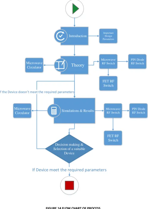
3. Simulations and Results
The following flow chart provides an overview of the whole report.
Introduction Important Design Parameters Microwave Circulator Microwave/ RF Switch PIN Diode RF Switch FET RF Switch
Simulations & Results
Theory Microwave Circulator Microwave/ RF Switch PIN Diode RF Switch FET RF Switch Decision making &
Selection of a suitable Device
If Device meet the required parameters
If the Device doesn t meet the required parameters
21
3.1 Simulations for Microwave Circulator
Simulation work for Microwave Circulator has been done using HFSS (High frequency Structured Simulation Software) and simulations for RF/Microwave switch were performed using Advanced Design System (ADS).
3.1.1 Experimental Design of Microwave circulator
According to the microwave circulator theory presented in chapter no. 2, the required parameters to design the circulator are calculated and used in circulator design process using HFSS. A finite element method is followed in the designing of circulator. The properties of the ferrite disk are given in the following table, these values are used in the circulator simulation process.
Property values
Disk thickness 0.35mm
FR4-Substrate Dielectric constant (𝝐𝒓) @ 3.125GHz
14.9
Saturation magnetization (4𝝅𝑴𝒔) 1675G FMR line width 50 A/m @ 3.125GHz
Electric & magnetic losses 0 Table 2. Substrate specification
Based on the operating frequency and the substrate related values, the radius of the ferrite disk is calculated by using the equation (21b) in Appendix. A certain amount of external magnetic field is applied (greater than the FMR region) in the direction normal to ferrite disk for the biasing. According to the equations (18) and (21a) in Appendix, the width of the micro strip line is calculated. All these parameters are tabulated below and are used in the circulator designing and simulation process.
Parameters values
Operating frequency (f) 3.125 GHz
Radius of the disk 1.5mm
Applied magnetic field 460000A/m
Width of the micro strip line 0.34mm Table 3. Ferrite disk specifications.
Based upon these calculations and properties of the ferrite, the circulator was designed using HFSS. The experimental model of the circulator is given in the following figure.
22
FIGURE 15. EXPERIMENTAL MODEL OF DIFFERENTIAL LINE MICRO-STRIP CIRCULATOR
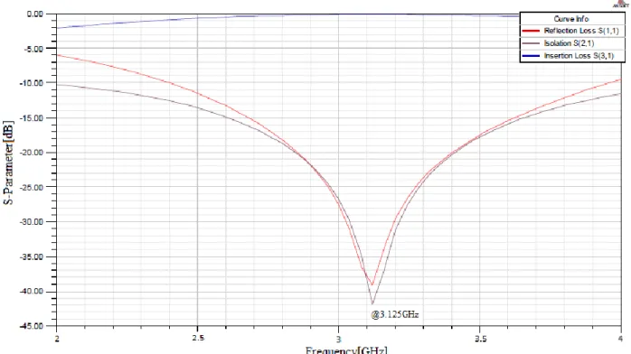
Simulations performed for the designed circulator and the results are obtained in terms of S – parameters (in dB) plot. These results are shown in Figure 16.
FIGURE 16. S-PARAMETERS OF THE SIMULATION MODEL
According to the above S-parameters plot, it is very clear that the transmission has occurred from port 1 to port 3 i.e. (𝑆31) and the isolation has occurred between port 1 and port 2 i.e. (𝑆21).
23 Here the blue curve represents the insertion loss (𝑆31), red curve represents the return loss (𝑆11) and the
gray curve represents the isolation (𝑆21).
The minimum insertion loss at the operating frequency is approximately -1.75dB (𝑆31= −1.75𝑑𝐵),
return loss (𝑆11= -11dB) and the isolation (𝑆21= −13𝑑𝐵).
These S-parameters are just good according to the theory, but at the same time, keeping in mind the bandwidth requirement in the communication system, these S-parameters are not enough.
These S-parameters are able to support only 5% bandwidth of the system, i.e. within this 5% BW, good transmission occurs.
However, most of the designs can be improved by tuning or optimizing the different parameters which are suitable to optimize. In this case, the micro strip line width (W) and the external applied magnetic field (H) can be used for tuning, while keeping other parameters like ferrite disk radius and thickness constant because the ferrite disk dimensions are hard to change in practical.
The optimization of the design is continued by tuning two parameters; The width of the micro strip line and
The applied magnetic field.
3.1.1.1
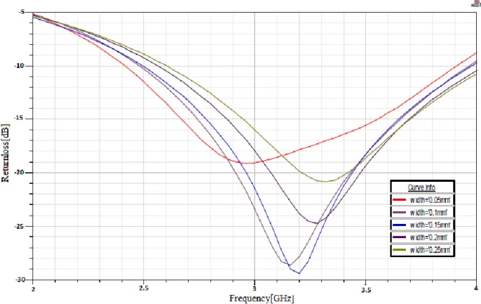
Optimization with different micro-strip line widths (W)
The specifications of different micro strip width and the design parameters which are kept constant are given in the following table
Parameter value
Width of micro strip line (W) 0.05mm to 0.25mm
Applied magnetic field (H) 460000A/m
Thick ness of the disk 0.35mm
Radius of the disk (R) 015mm Table 4. Micro-strip width specifications
Using the different micro strip widths from 0.05mm to 0.25mm, again the simulations of the circulator is performed and its related S-parameters (𝑆31, 𝑆11 & 𝑆21) are obtained in individual plots.
Where
24
FIGURE 17. INSERTION LOSS (S31) PLOT USING DIFFERENT WIDTHS OF MICRO-STRIP LINE
25
FIGURE 19. ISOLATION (S21) PLOT USING DIFFERENT WIDTHS FOR MICRO-STRIP LINE
S-parameter At 3.125GHz @ 15% - BW
𝑺𝟑𝟏 -0.18dB
𝑺𝟏𝟏 -28dB
𝑺𝟐𝟏 -30dB
Table 5. Optimized results
According to the 1st step of Optimization, three individual plots are obtained. Figure 17 gives the optimized insertion loss (𝑆31) information, Figure 18 gives the optimized return loss (𝑆11) information
and the Figure 19 gives the optimized isolation (𝑆21) information. All these optimized results occurred
at different micro strip widths.
From Figure 17, it is clear that good insertion loss is obtained at a width (W) of 0.15mm and the loss is approximately -0.18dB at the operating frequency 3.125GHz. Also a good transmission occurs for a good bandwidth (15%) coverage in between 2.9GHz to 3.4GHz.
From Figure 18, also a good return loss occurred at the same width (W) of 0.15mm, the loss is approximately -28dB at the operating frequency. Since the application is a wide-band communication system, the return loss doesn’t satisfy the bandwidth requirement. The return loss is good over 10%
26 BW. An optimization is still required regarding the return loss S-parameter to cover more bandwidth of the system.
From Figure 19, a good Isolation occurred at the same width (W) of 0.15mm, the isolation is approximately -30dB at the operating frequency. Considering the application, a good isolation has occurred only over 10% bandwidth of the system. An optimization is still required regarding the isolation S-parameter to cover more bandwidth of the system. Now the 2nd step of optimization is continued by changing the external magnetic fields applied.
3.1.1.2
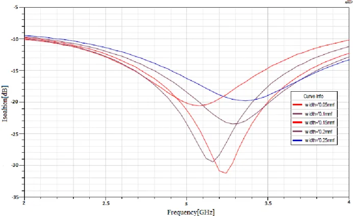
Optimization with different applied Ho fields
The specifications of different applied magnetic fields and the design parameters which are kept constant in the optimization process is given in the following table
Parameter Value
Width of micro strip line (W) 0.15mm (optimized)
Applied magnetic field (H) 520000 to 560000A/m
Thick ness of the disk 0.35mm
Radius of the disk (R) 0.15mm Table 6. Specification for different applied magnetic fields
By using these different applied magnetic fields, the optimized simulations of the circulator are again performed to improve the system bandwidth requirement.
27
FIGURE 20. INSERTION LOSS (S31) USING DIFFERENT HO FIELDS
28
FIGURE 22. ISOLATION (S21) USING DIFFERENT HO FIELDS
S-parameter At 3.125GHz @ 20% - BW
𝑺𝟑𝟏 -0.182dB
𝑺𝟏𝟏 -39dB
𝑺𝟐𝟏 -42dB
Table 7. Optimized results
According to the 2nd step of Optimization, three individual plots are obtained. Figure 20 gives more optimized insertion loss (𝑆31), Figure 21 gives the return loss (𝑆11) information and the Figure 22 gives
the isolation (𝑆21) information. All these optimized results occurred at different magnetic fields applied
externally.
From Figure 20, it is clear, that the good insertion loss is obtained at 540000 A/m magnetic field and the loss is approximately -0.182dB at the operating frequency 3.125GHz. Also a good transmission occurs over 20% bandwidth coverage, i.e. 2.7GHz to 3.4GHz.
From Figure 21, also a good return loss occurred at the same magnetic field applied, the loss is approximately -39dB at the operating frequency. Since the application is a wide-band communication system, the return loss is minimized to satisfy the bandwidth requirement. The return loss is good over 20% BW.
From Figure 22, a good Isolation occurred at the same magnetic field applied by, the isolation is approximately -42dB at the operating frequency. Considering the application, a good isolation has
29 occurred over 20% bandwidth of the system. An optimization is still required regarding the isolation S-parameter to cover more bandwidth of the system.
To be able to obtain even more bandwidth coverage, the two well optimized parameters (W &𝐻0) are
used in further step.
3.1.1.3
Optimized S-parameters
From the above two optimized steps, the micro strip width, magnetic field specifications are finalized and the design parameters are used in the further simulation process.
Parameter Value
Micro strip width (W) 0.5mm
Magnetic field (𝑯𝟎) 540000 A/m Disk radius (R) 0.15mm
Disk thickness 0.35mm Table 8. Finalised specifications
FIGURE 23. OPTIMIZED S-PARAMETERS OF THE SIMULATION MODEL
S-parameter At 3.125GHz --- 25% - BW
𝑺𝟑𝟏 -0.082dB
𝑺𝟏𝟏 -39dB
𝑺𝟐𝟏 -42dB
30 From the tuning part, the best design parameters are selected and good S-parameters are achieved by the optimization and a good bandwidth (25%) coverage is obtained according to the tuned design parameters.
According to Figure 23, the minimum insertion loss -0.082dB is obtained at the operating frequency, the return loss is minimized to -39dB and the isolation is greatly improved to -42dB.
All these optimized S-parameters covered 25% bandwidth of the system, which is generally a good coverage in wideband communication systems but here the circulator has been designed by assuming zero electric and magnetic losses. In reality, the insertion loss could be even more than what has been achieved. So, all these parameters and ferrite properties set a bandwidth limit.
3.2 Simulations for PIN diode Switch
In the following sections, SPDT switch configurations using PIN diode are given. In all these topologies, two of the terms will be used quite frequently, so, it is important to highlight these two terms. First one is “transmission mode”. “Transmission mode” refers to the state of the switch, where it is used for signals to be transmitted from transmitter to antenna having receiver port being isolated from transmitter port and antenna port. Second term “reception mode” indicates the state of the RF switch, where it is desired to route the signal from antenna port to the receiver port having transmitter port completely isolated from antenna and receiver port.
3.2.1 Series PIN SPDT Switch
It is the very basic configuration of an RF SPDT switch using PIN diodes. Its schematic is given in Figure 24. D1 D2 TX port RX port Ant port DC block DC block RF choke RF choke DC DC
FIGURE 24. SERIES PIN SPDT SWITCH DESIGN
Series PIN SPDT configuration gives low insertion loss and relatively high isolation. It works for wide bandwidths since there is no frequency dependant element present in the design. It works in a way that
31 PIN diode between the two ports intended to have low insertion loss between them, is forward biased, and ports where isolation is required, PIN diode is reversed biased. Limitation of this design is that the power handling of series connected PIN diodes is poor, so it results in loss in power transmission from one port to another port. During the transmission mode, diode D1 is forward biased and D2 is reversed biased. Forward biased D1 provides low resistance 𝑅𝑠 between antenna and transmitter port, so RF
signal finds its way from the transmitter directly to the antenna. Isolation between antenna and receiver port is achieved by reverse biasing the diode D2. Similarly, during reception mode, when signal is intended to go from antenna port to receiver port, polarities of DC-bias are reversed.
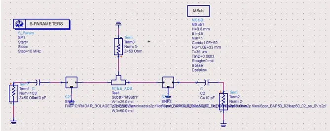
So, to get better idea how above configuration works with real life PIN diodes, PIN diode’s s2p models were used to perform simulations. Following is the schematic for series PIN switch using s2p models.
FIGURE 25.SIMULATION SETUP FOR SERIES PIN SPDT SWITCH USING S2P MODELS
HPND-4028 and HPND-4038 PIN diode models were used in the above setup. These two PIN diodes were chosen because of their low resistance in forward bias, low capacitance in reverse bias-mode and fast switching speed. Results obtained for insertion loss, isolation and return loss for both of these diodes are given as below.
32
FIGURE 26. TRANSMISSION AND RECEPTION MODE RESULTS
Transmission mode Reception mode
Tx-Ant. (insertion loss) @ 𝒇𝒐 -0.226dB Tx-Ant. (isolation) @ 𝒇𝒐 -25dB Tx-Rx (isolation) @ 𝒇𝒐 -30dB Tx-Rx (isolation) @ 𝒇𝒐 -25dB Ant.-Rx (isolation) @ 𝒇𝒐 -29dB Ant.-Rx (insertion loss) @ 𝒇𝒐 -0.121dB
Return loss @ 𝒇𝒐 -32dB Return loss @ 𝒇𝒐 -40dB
Bandwidth (2GHz) 64% of 𝒇𝒐 Bandwidth (2GHz) 64% of 𝒇𝒐
TABLE 10. RESULTS: SERIES PIN SPDT SWITCH USING S2P MODELS
From the above results, it is visible that for both transmission mode and reception mode of the RF switch, HPND-4028 and HPND-4038 PIN diodes performed pretty well and insertion loss, return loss and isolation levels are quite realizable. Please be advised that this design gave good results for bandwidth more than 2GHz, but only 2GHz bandwidth results are shown in Figure 26. Though, series PIN diode switch configuration has given good results, to achieve higher levels of isolation, PIN diodes are used in the shunt configuration which is discussed in the next section.
33
3.2.2 Shunt PIN SPDT Switch
Shunt PIN Single pole double throw (SPDT) switch has following schematic.
TX port RX port
Ant port
DC block DC block
RF choke RF choke
DC DC
λ/4 transmission line λ/4 transmission line
D1 D2
FIGURE 27. SHUNT PIN SPDT SWITCH DESIGN
This configuration is intended to provide high isolation. Switch is turned on by reverse biasing the diodes which provides high capacitance. However, shunt diodes switches have narrow bandwidth because of the use of quarter wave transmission lines. In the transmission mode, diode D1 is reversed biased and D2 is forward biased, RF signal will flow from port 1 to port 3 and port 2 will be isolated. Quarter wave line will transform the short circuit at D2 to an open circuit at common junction point (90° transform) [21]. When RF signal sees open circuit towards receiver port, it allows all the power to be transmitted from transmitter to antenna. Similarly, for the reception mode, polarities of biasing voltages are reversed to make port 1 (transmitter) isolated. Despite of its high isolation properties, this design has a drawback that when frequency is changed from its centre frequency, 𝜆/4 lines tend to change their electrical length which in turn creates mismatch at common junction.
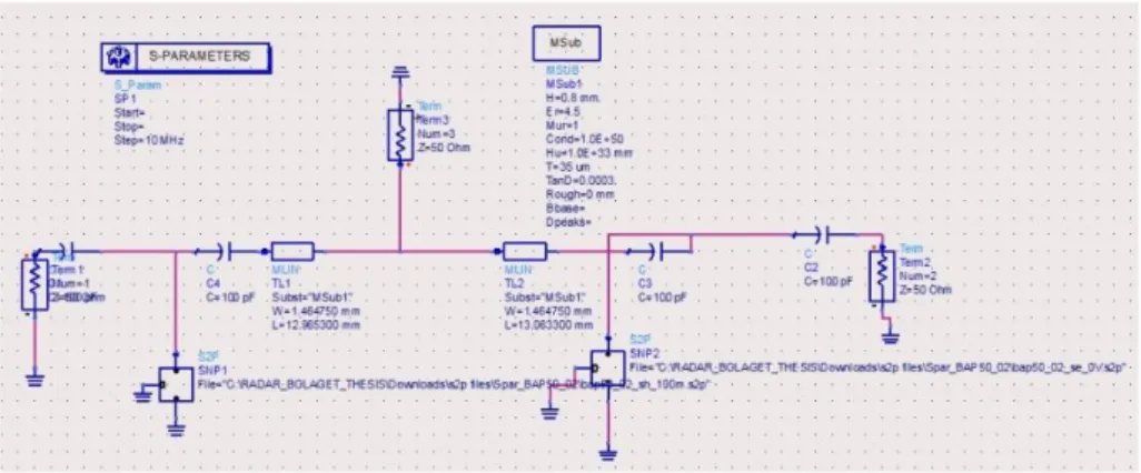
Shunt PIN diode configuration was simulated using s2p models for PIN diodes HPND_4028 and HPND_4038 for transmission and receiving mode respectively. Schematic used for this task is as under.
34 Substrate specifications for this setup are as follow.
𝐶𝑒𝑛𝑡𝑟𝑒 𝑓𝑟𝑒𝑞𝑢𝑒𝑛𝑐𝑦 = 3.125𝐺𝐻𝑧 𝑆𝑢𝑏𝑠𝑡𝑟𝑎𝑡𝑒 𝑢𝑠𝑒𝑑 = 𝐹𝑅4 𝑆𝑢𝑏𝑠𝑡𝑟𝑎𝑡𝑒 𝑡ℎ𝑖𝑐𝑘𝑛𝑒𝑠𝑠 = 0.8𝑚𝑚 𝑅𝑒𝑙𝑎𝑡𝑖𝑣𝑒 𝑑𝑖𝑒𝑙𝑒𝑐𝑡𝑟𝑖𝑐 𝑐𝑜𝑛𝑠𝑡𝑎𝑛𝑡 = 4.5 𝑅𝑒𝑙𝑎𝑡𝑖𝑣𝑒 𝑝𝑒𝑟𝑚𝑒𝑎𝑏𝑖𝑙𝑖𝑡𝑦 = 1 𝐶𝑜𝑛𝑑𝑢𝑐𝑡𝑜𝑟 𝑐𝑜𝑛𝑑𝑢𝑐𝑡𝑖𝑣𝑖𝑡𝑦 = 1.0𝐸 + 50 𝐶𝑜𝑣𝑒𝑟 ℎ𝑒𝑖𝑔ℎ𝑡 = 1.0𝐸 + 33𝑚𝑚 𝐶𝑜𝑛𝑑𝑢𝑐𝑡𝑜𝑟 𝑡ℎ𝑖𝑐𝑘𝑛𝑒𝑠𝑠 = 35𝜇𝑚 𝐷𝑖𝑒𝑙𝑒𝑐𝑡𝑟𝑖𝑐 𝑙𝑜𝑠𝑠 𝑡𝑎𝑛𝑔𝑒𝑛𝑡 = 0.0003 𝑅𝑜𝑢𝑔ℎ = 0𝑚𝑚
Results obtained for two s2p models are shown in Figures below.
35
Results are presented in tabular form in Table 11.
Transmission mode Reception mode
Tx-Ant. (insertion loss) @ 𝒇𝒐 -0.229dB Tx-Ant. (isolation) @ 𝒇𝒐 -20B Tx-Rx (isolation) @ 𝒇𝒐 -20dB Tx-Rx (isolation) @ 𝒇𝒐 -20dB Ant.-Rx (isolation) @ 𝒇𝒐 -19dB Ant.-Rx (insertion loss) @ 𝒇𝒐 -0.129dB
Return loss @ 𝒇𝒐 -34dB Return loss @ 𝒇𝒐 -34dB
Bandwidth (2GHz) 64% of 𝒇𝒐 Bandwidth (2GHz) 64% of 𝒇𝒐
TABLE 11. RESULTS: SHUNT PIN SPDT SWITCH
Though, shunt PIN diode switch was supposed to give higher isolation levels than series PIN diode configuration, but s2p models were not proved to be quite impressive when used in shunt PIN configuration. One thing important to mention here is that the use of quarter wave transmission line makes shunt PIN diode switch narrow band.
This limitation in isolation level can be improved by using a blend of series PIN diode configuration and shunt PIN diode configuration. This is called series-shunt PIN diode switch configuration.
3.2.3 Series-shunt PIN SPDT Switch
Series-shunt PIN SPDT switch topology was designed aiming to have insertion loss characteristics of series PIN diode switch and isolation characteristics of shunt PIN diode configuration. Its schematic is given in Figure 30. TX port RX port Ant port DC block DC block RF choke RF choke DC DC D1 D2 D3 D4
FIGURE 30. SERIES-SHUNT PIN SPDT SWITCH DESIGN
𝑅𝑠 and 𝐶𝑗 values are chosen to be 1.5Ω and 0.045pF respectively in accordance with the data sheet of
PIN diode HPND-4038. During transmission, diodes D2 and D3 are forward biased and diodes D1 and D4 are reversed biased. Polarities are reversed during reception mode. Simulation setup was created in ADS which is shown in figure below. S2p models used were HPND-4028, HPND-4038.
36
FIGURE 31. SIMULATION SETUP FOR SERIES-SHUNT PIN SPDT SWITCH USING S2P MODELS
Results obtained with this simulation setup are depicted in Figure 32.
FIGURE 32. TRANSMISSION AND RECEPTION MODE RESULTS
Transmission mode Reception mode
Tx-Ant. (insertion loss) @ 𝒇𝒐 -0.119dB Tx-Ant. (isolation) @ 𝒇𝒐 -71B Tx-Rx (isolation) @ 𝒇𝒐 -71dB Tx-Rx (isolation) @ 𝒇𝒐 -71dB Ant.-Rx (isolation) @ 𝒇𝒐 -71dB Ant.-Rx (insertion loss) @ 𝒇𝒐 -0.119dB
Return loss @ 𝒇𝒐 -34dB Return loss @ 𝒇𝒐 -34dB
Bandwidth (2GHz) 64% of 𝒇𝒐 Bandwidth (2GHz) 64% of 𝒇𝒐
TABLE 12. RESULTS: SERIES-SHUNT PIN SPDT SWITCH
From the above results, it is evident that series-shunt PIN diode switch design has given pretty impressive results with s2p models. However, series-shunt PIN diode is bit complex to design and requires higher biasing current and power as compared to series and shunt configuration.
37 It is interesting to note in all above designs, that biasing circuit and RF circuit share the same path for signal transmission which makes it quite vulnerable to distortion. To avoid DC being entering into the RF ports, DC blocks are used at each port. Unfortunately, besides blocking DC, these capacitors also degrade insertion loss performance of switch due to high pass filter effect [3]. Furthermore, to isolate DC bias circuit from high frequency RF signal, RF chokes are used in series with DC voltage source. All three topologies presented above are discussed in [3].
Having discussed above three PIN diode SPDT switch topologies, it is evident that all these three topologies gave realisable results with the isolation as much as -71dB (in case of series-shunt SPDT switch) and insertion loss of < 0.5dB. In section 3.2.4, a PIN diode switch design is presented which is able to achieve even higher isolation level yet only requires one biasing circuit.
3.2.4 Very High Isolation Switch
Switch topology intended to be presented in this section is designed using HSMP-386x series PIN diodes which has two major applications; attenuators and switches. In switch design, low capacitance is the driving design consideration and HSMP-386x series diodes find their way in such applications because of their low capacitance. In this very configuration, SOT 323 package is used (this configuration is available in HSMP-386x series data sheet) [23]. Schematic for this design is shown in Figure 33. Antenna port Tx port Rx port D3 D4 D1 D2 D5 D6 DC
FIGURE 33. VERY HIGH ISOLATION SWITCH DESIGN
Design presented in Figure 33 requires only one biasing circuit and operates as follow. During transmission mode, DC voltage source is ‘on’ (3V-5V), which turns diode D1, D4 and D5 to on-state (low resistance). RF signal easily flows from transmitter port to antenna port. Any leaked RF signal trying to enter the isolated receiver port will be shunted away by D5 or RF signal will be totally blocked
38 by the open circuit created by off-state diode D6. Reception mode mechanism works in the opposite way and requires the control voltage to be at 0V to 0.5V.
S2p models will now be implemented to verify this design to be practicable. S2p model simulation setup is designed using ADS is shown below in Figure 34.
FIGURE 34. SIMULATION SETUP FOR VERY HIGH ISOLATION SWITCH USING S2P MODELS
Results obtained are presented in following figure.
FIGURE 35. TRANSMISSION AND RECEPTION MODE RESULTS
Tabular form of results are presented in Table 13 for better visual. The above configuration proved to be the best one discussed so far. It is broad-band design, able to give pretty impressive insertion loss, isolation and return loss results over a 10GHz band. Moreover, it required only one biasing circuit which made it quite efficient in terms of power consumption as it does not require any power source during reception mode.
39
Transmission mode Reception mode
Tx-Ant. (insertion loss) @ 𝒇𝒐 -0.223dB Tx-Ant. (isolation) @ 𝒇𝒐 -79dB Tx-Rx (isolation) @ 𝒇𝒐 -79dB Tx-Rx (isolation) @ 𝒇𝒐 -79dB Ant.-Rx (isolation) @ 𝒇𝒐 -79dB Ant.-Rx (insertion loss) @ 𝒇𝒐 -0.22dB
Return loss @ 𝒇𝒐 -30dB Return loss @ 𝒇𝒐 -31dB
Bandwidth 10GHz Bandwidth 10GHz
TABLE 13. RESULTS: VERY HIGH ISOLATION SWITCH
3.3 Simulations for FET Switch
As discussed in section 2.3.2.4, when 𝑉𝐺𝑆 is greater than the threshold voltage of the FET, FET turns to
its on-state, and when the applied 𝑉𝐺𝑆 is less than the threshold voltage of a particular FET, FET remains
in its off-state. Threshold voltage is positive for enhancement-type FETs and negative for depletion-type FETs. Let’s take a quick view of enhancement-depletion-type and depletion-depletion-type FETs. Please be advised that detail of these two types are not covered in this report, just a brief definition is presented to be able to make the reader understand the difference between these two types, as for the simulation purpose, enhancement-type FET is used throughout this report. Enhancement-type FET is the one, which has no conduction channel present when there is no 𝑉𝐺𝑆 applied. Conduction channel is only formed with the
applied 𝑉𝐺𝑆, and the width of conduction channel, and as a result, the current through the channel, can
be increased by increasing 𝑉𝐺𝑆. On the other hand, depletion-type FET is the one, which has already a
conduction channel present between source and drain terminals even when there is no 𝑉𝐺𝑆 applied. So,
in this case, 𝑉𝐺𝑆 has to be reversed biased or made more negative to reduce the channel width and as a
result to limit the amount of current flowing through the channel [16]. Furthermore, FETs when used in amplifier applications, Q-point or operating point needed to be find out for proper biasing of FET, however, the only biasing required for FET in RF switches is the level of 𝑉𝐺𝑆 which can turn the FET
“on” or “off”. So, the term, ‘biasing circuit’ or ‘control voltage’, always refers to the 𝑉𝐺𝑆.
The above mentioned properties of FET make it a wonderful choice to be used in applications like RF/Microwave switches. In the on-state, channel resistance, 𝑅𝐷𝑆, is very small allowing considerable
amount of current to flow and when 𝑉𝐺𝑆 is reversed biased to turn the FET to its off-state, 𝑅𝐷𝑆 value
becomes quite high, obstructing the flow of current through the channel. This property of FET enables it to provide pretty good isolation at low frequency. On the contrary, the isolation is limited by the capacitance between the Source and Drain terminal; 𝐶𝐷𝑆. So, a balance between the 𝑅𝐷𝑆 and 𝐶𝐷𝑆 should
be used in order to get desirable insertion loss and isolation [24]. By knowing the values of 𝐶𝐷𝑆 and
𝑅𝐷𝑆, one can estimate the levels of insertion loss and isolation. Let’s use for example
𝐷𝑟𝑎𝑖𝑛 𝑡𝑜 𝑆𝑜𝑢𝑟𝑐𝑒 𝑖𝑚𝑝𝑒𝑑𝑎𝑛𝑐𝑒, 𝑅𝐷𝑆 = 2Ω
![FIGURE 10. FET FAMILY TREE [18]](https://thumb-eu.123doks.com/thumbv2/5dokorg/4632457.119811/24.892.225.668.323.600/figure-fet-family-tree.webp)