Doctoral Thesis in Physics
Metal-assisted chemical etching
for nanofabrication of hard
X-ray zone plates
RABIA AKAN
Doctoral Thesis in Physics KTH Royal Institute of Technology Stockholm, Sweden 2021
Academic Dissertation which, with due permission of the KTH Royal Institute of Technology, is submitted for public defence for the Degree of Doctor of Philosophy on Friday the 30th April 2021, at 10:00 a.m. in Zoom and BioX Library, Roslagstullbacken 21, Stockholm.
TRITA-SCI-FOU 2021:09
Commonly used optics in nanoprobes for high resolution X-ray experiments are zone plates.
Zone plates are circular diffraction optics with radially decreasing grat-ing periods. Their performance depends on their geometrical properties and material. The width of the outermost zone, which today is in the order of a few tens of nanometers, defines the zone plate resolution, while the zone thickness and the material define the ray focusing efficiency. For hard X-ray zone plates, the required zone thickness is several micrometers. There-fore, high-aspect ratio nanostructures are a prerequisite for high-resolution, high-efficiency zone plates. The very small structures together with the high-aspect ratios make zone plates one of the most challenging devices to fabricate. A wet-chemical nanofabrication process that has proved its ca-pability of providing silicon nanostructures with ultra-high aspect ratios is metal-assisted chemical etching (MACE). MACE is an electroless, autocat-alytic pattern transfer method that uses an etching solution to selectively etch a predefined noble metal pattern into silicon. In this thesis, MACE is optimized specifically for zone plate nanostructures and used in the devel-opment of a new zone plate device nanofabrication process.
The MACE optimization for silicon zone plate nanostructures involved a systematic investigation of a wide parameter space. The preferable etching solution composition, process temperature, zone plate catalyst design and silicon type were identified. Parameter dependencies were characterized with respect to etching depth and verticality, mechanical stability of zones and silicon surface roughness.
Zone plate molds with aspect ratios of 30:1 at 30 nm zone widths were nanofabricated using the optimized MACE process. For use with hard X-rays, the silicon molds were metallized with palladium using electroless de-position (ELD). The first order diffraction efficiency of such a palladium/sil-icon zone plate was characterized as 1.9 %. Both MACE for the zone plate pattern transfer and ELD for the silicon mold metalization are conceptu-ally simple, relatively low-cost and accessible methods, which opens up for further developments of zone plate device nanofabrication processes.
Sammanfattning
Hårdröntgensvepmikroskopi möjliggör avbildandet av prover och karaktä-risering av dem kemiska, elementära och strukturella egenskaperna med nanometerupplösning. Detta är tack vare användandet av nanofokuserande optik. Vanligen förekommande optik i röntgenmikroskop för högupplösta analyser är zonplattor.
Zonplattor är cirkulära diffraktionsoptik med radiellt avtagande gitter-period. Deras prestanda beror på de geometriska egenskaperna och materi-alet de är gjorda av. Bredden på den yttersta zonen, vilken vanligtvis är i storleksordningen av några tiotal nanometer, definierar zonplattans optiska upplösning medan zontjockleken samt dess material definierar verkningsgra-den. För hårdröntgenzonplattor krävs ofta en zontjocklek på några mikro-meter. Detta gör nanostrukturer med stort tjocklek-breddförhållande en för-utsättning för högupplösta zonplattor med hög verkningsgrad. De väldigt små strukturerna och det stora tjocklek-breddförhållandet gör zonplattor utmanande att tillverka.
En våtkemisk nanofabrikationsprocess som har påvisat sin förmåga att tillverka kiselnanostrukturer med extrema tjocklek-breddförhållanden är metall-assisterad kemisk etsning (MACE). MACE är en elektrofri, auto-katalytisk process där fördefinierade ädelmetallstrukturer med hjälp av en etslösning selektivt etsar kisel. I denna avhandling optimeras MACE speci-fikt för nanometerstora zonplattestrukturer och används i en ny nanofabri-kationsprocess utvecklad för framtagning av zonplattor.
Optimeringen av MACE för zonplattestrukturer i kisel utgjordes av en systematisk och omfattande parameterstudie. Den bättre kompositionen av etslösningen, processtemperaturen, zonplattedesignen och kiselsubstra-tet identifierades. Processen karaktäriserades med avseende på zonplattans tjocklek och etsriktningen, den mekaniska stabiliteten av zoner och ytråhe-ten hos kislet.
Kiselzonplattor med ett tjocklek-breddförhållande på 30:1 med en mins-ta zonbredd på 30 nm tillverkades med den optimerade MACE processen. Inför användning med hårdröntgen metalliserades kiselzonplattorna med palladium via en autokatalytisk pläteringsprocess (ELD). Verkningsgraden av första ordningens diffraktion för en sådan palladium/kiselzonplatta ka-raktäriserades till 1.9 %. Både MACE och ELD är konceptuellt enkla, rela-tivt låga i kostnad och tillgängliga metoder som kommer bana väg för det vi-dare utvecklandet av nanofabrikationsprocesser för zonplatteframställning.
control of metal-assisted chemical etching for silicon-based zone plate nanos-tructures, RSC Adv. 8, 12628 (2018).
Paper B
R. Akan, K. Parfeniukas, C. Vogt, M. S. Toprak and U. Vogt, Investigation
of metal-assisted chemical etching for fabrication of silicon-based X-ray zone plates, Microscopy and Microanalysis 24, 286 (2018).
Paper C
R. Akan, T. Frisk, F. Lundberg, H. Ohlin, U. Johansson, K. Li, A. Sakd-inawat, and U. Vogt, Metal-assisted chemical etching and electroless
depo-sition for fabrication of hard X-ray Pd/Si zone plates, Micromachines 11,
301 (2020). Paper D
R. Akan and U. Vogt, Optimization of metal-assisted chemical etching for
deep silicon nanostructures, manuscript, (2021).
Paper E
K. Parfeniukas, S. Giakoumidis, R. Akan and U. Vogt, High-aspect ratio
zone plate fabrication for hard X-ray nanoimaging, Proc. SPIE 10386,
List of abbreviations
AFM Atomic force microscopy ALD Atomic layer deposition
CS Central stop
DI Deionized
DRIE Deep reactive ion etching EBL Electron beam lithography
ED Electrodeposition
ELD Electroless deposition
FIB Focused ion beam
HSQ Hydrogen silsesquioxane
ICP-OES Inductively coupled plasma optical emission spectrometry
IPA Isopropanol
MACE Metal-assisted chemical etching MLL Multilayer Laue lens
OSA Order sorting aperture PMMA Poly(methyl methacrylate) RIE Reactive ion etching
Contents
Abstract iii Sammanfattning iv List of papers v List of abbreviations vi 1 Introduction 1 1.1 Nanostructured silicon . . . 11.2 Objective of the thesis . . . 2
1.3 Outlines of this thesis . . . 2
2 NanoMAX: the hard X-ray nanoprobe of MAX IV 5 2.1 Hard X-ray nanoprobes . . . 5
2.1.1 Focusing optics . . . 6
2.1.2 Operation modes . . . 6
2.2 The nanofocusing zone plate station at NanoMAX . . . 7
3 Zone plate optics 9 3.1 Zone plate theory . . . 9
3.2 Zone plates for the hard X-ray range . . . 12
3.3 Fabrication methods . . . 14
3.3.1 Direct-write processes . . . 15
3.3.2 Etching processes . . . 15
4 Metal-assisted chemical etching: theoretical background 17 4.1 The etching process . . . 17
4.2 Mass-transport models . . . 20
4.3 Etching solution . . . 20
4.4 Temperature . . . 22
4.6 Silicon . . . 23
5 Nanofabrication of silicon-based zone plates 25 5.1 Zone plate design, patterning and deposition in gold . . . 25
5.2 Pattern transfer with metal-assisted chemical etching . . . 29
5.3 Metalization methods . . . 30
5.3.1 Palladium electroless deposition . . . 31
5.3.2 Gold electrodeposition . . . 33
5.4 Substrate back-thinning . . . 34
6 Optimization of metal-assisted chemical etching for zone plate nanostructures 37 6.1 Etching solution composition . . . 38
6.2 Processing temperature . . . 40
6.3 Zone plate catalyst design . . . 41
6.4 Silicon type . . . 44
7 Zone plate efficiency characterization 47 7.1 Experimental setup . . . 47
7.2 First order diffraction efficiency quantification . . . 48
8 Conclusions and outlook 51
Summary of papers 53
Acknowledgements 55
Chapter 1
Introduction
1.1 Nanostructured silicon
The research fields of medicine [1], photonics [2,3], thermoelectrics [4], pho-tovoltaics [5, 6], energy storage [7, 8] and X-ray optics [9] might at the first glance seem very distant from each other. What could possibly be the common denominator that gathers thermoelectric materials, membranes for drug delivery and Fresnel zone plates in the same list? The answer is nanostructured silicon.
By accident, porous silicon was discovered by Arthur Uhlir and Ingeborg Uhlir in 1956 during one of their electro-polishing experiments [10]. The dis-covery found great attention years later, in the early 1990s, when Canham reported a strong and bright photoluminescence from porous silicon at room temperature [11]. Since then, different fabrication methods for this inter-esting nanostructured material have been investigated. In 1997, the first report came of an electroless etching method catalyzed by aluminium for the selective formation of porous silicon layers in an acid-mixture consisting of nitric and hydrofluoric acid [12]. Shortly after, the aluminium was ex-changed to a noble metal that stayed inert in an etching solution composed of hydrogen peroxide and hydrofluoric acid and produced porous silicon de-fined by the morphology of the noble metal catalyst [13]. This report by Li and Bohn is considered as the first study that introduced metal-assisted chemical etching (MACE, MacEtch or MAE), not only as a method to form porous silicon, but silicon with defined 3D nano- and micro-structure mor-phology. Since its discovery, MACE has shown its diversity and capability as a new method for the fabrication of advanced silicon structures for a wide range of applications that require high aspect ratios, i.e., structures with large thicknesses in relation to their structural widths [14–16].
nanostruc-tures are a special type of X-ray optics: Fresnel zone plates [17, 18]. For the fabrication of hard X-ray zone plate optics, nanostructures around tens of nanometers with lengths of several micrometers and aspect ratios of at least 30:1 are needed. Zone plate devices are commonly used in hard X-ray scanning microscopes as imaging and nanofocusing optics [19]. Hard X-ray microscopy enables non-invasive analysis of matter, where not only information about the surface of an object can be gathered but also its interior. Probing properties of matter at nanoscale, or even atomic scale resolution would help us understand and answer important questions in ma-terials science, life science, earth science, nanoscience and many others. The limitations in the achievable aspect ratios of these optics has been the lim-iting factor at what scale analyses can be performed with X-ray microscopy. The optical resolution of such a tool depends on the size of the focused X-ray spot which is defined by the structural sizes of the zone plate. Processes for high-aspect ratio zone plate structures are needed for the continued de-velopment of hard X-ray microscopy. And this is exactly what we try to do in this thesis: process development for the nanofabrication of high-aspect ratio zone plate nanostructures using MACE for the improvement of hard X-ray scanning microscopy.
1.2 Objective of the thesis
This thesis work aims to explore MACE as a pattern transfer method to fab-ricate high-aspect ratio silicon nanostructures, specifically zone plates. The objective is to identify the dependencies between experimental MACE pa-rameters and etching verticality, mechanical stability and silicon wall rough-ness and optimize the process for the development of a zone plate device nanofabrication process.
1.3 Outlines of this thesis
After the present introduction, this thesis is structured as follows.
Chapter 2 introduces the concept of X-ray scanning microscopy and gives a general overview of such a setup. NanoMAX, the hard X-ray nanoprobe of MAX IV, is presented and its nanofocusing zone plate station is described. Chapter 3 covers the basic theory about zone plate optics. Their required properties to function with hard X-rays are detailed and an overview of the commonly used fabrication processes are listed. Recent advances in the nanofabrication field are presented, including MACE.
Chapter 4 provides a theoretical background about MACE and discusses the expected influence of the involved process parameters on the etching behaviour.
Chapter 7 summarizes the first order diffraction efficiency characteriza-tion of the zone plate devices fabricated via the developed nanofabricacharacteriza-tion process.
Chapter 8 concludes this thesis work and gives a brief outlook on poten-tial developments for the future.
Chapter 2
NanoMAX: the hard X-ray
nanoprobe of MAX IV
Hard X-ray scanning microscopy is an imaging- and analysis method that enables sample imaging and probing their properties at the nanoscale. This combination makes hard X-ray microscopy attractive to various fields of physics, chemistry and biology, including materials science, life science, earth science, nanoscience and many others. Thanks to the large penetra-tion depth of X-rays, hard X-ray microscopy has the strength of examining the sample interior without any need for destructive sample preparation. All this is possible by illuminating the sample with a nanofocused, hard X-ray spot. This chapter introduces the concept of hard X-ray scanning micro-scopes, also called nanoprobes, and focuses especially on the NanoMAX beamline at MAX IV.
2.1 Hard X-ray nanoprobes
The main components of an X-ray nanoprobe are an X-ray light source, optic to produce an intense spot and focus the photons on the sample, a scanning stage holding the sample and a detector to record an image or other sample properties. Synchrotron facilities are typically used as X-ray sources in high performance nanoprobes due to their capability to deliver stable X-ray beams with high flux. In practice, a synchrotron light source could be used to perform transmission imaging of an object without the use of any optical device. However, optics are necessary to probe local sample properties at nanoscale resolution. For this, reflective, refractive and diffractive optics are used.
2.1.1 Focusing optics
Kirkpatrick-Baez (KB) mirrors are widely used at synchrotron facilities and focus the incoming beam by reflection in both horizontal and vertical direc-tions [20]. The advantage of this arrangement is the high focusing efficiency that can reach up to 90% [21]. However, the size of the focused X-ray spot is limited to around 100 nm at hard X-ray energies of 10 keV and lower [22]. Refractive optics, or lenses, have also been proposed as nanofocusing optics [23]. Due to the impractically long focal length of a single lens, stacking of multiple lenses or compound lens setups have been used [24, 25]. Multiple lenses etched into a single device gives short focal lengths, but severely limits the focusing efficiency. To avoid absorption losses, light atomic number materials are used for lenses [26].
Fresnel zone plates [17] and Multilayer Laue lenses (MLLs) [27] are two types of diffractive optics. Zone plates are circular gratings with radially decreasing line width so that the X-rays are diffracted into a common fo-cal point (described in more detail in Chapter 3) [28]. Their high reso-lution and ease-of-use make zone plates often the optics of choice at syn-chrotron nanoprobes, however, with a disadvantage of low focusing effi-ciency. The maximum theoretical efficiency of standard hard X-ray zone plates is 40% [29]. Frequent improvements in nanofabrication tools and processes are nonetheless pushing the limits of achievable resolution and practical efficiency of zone plates.
As the name suggests, MLLs consist of multiple layers of alternating ma-terials with decreasing thicknesses over the device. A large number of layers are required in these devices, which can be in 1D or 2D. The fabrication is the biggest limitation here due to the required accurate control during de-position of the materials. However, MLLs can be fabricated with arbitrary thicknesses, nanometer sized layers and even tilted zones, overcoming the diffraction efficiency and resolution limits of normal zone plates [30]. 2.1.2 Operation modes
Nanoprobes are highly flexible tools that can be operated in several modes to record chemical, elemental and structural information about both the surface and interior of a sample as a function of sample position [18]. Trans-mission spectrum analysis, also referred to as spectromicroscopy, records the X-ray absorption at a set wavelength and yields spectroscopic information. Within a heterogeneous sample, the chemical state and coordination number of an element can be analyzed while structural imaging of relatively thick samples can be done [31]. Fluorescence is a second operation mode [32]. Here, the elemental composition of a sample can be examined by analyzing the resulting emission caused by the incident X-ray beam. A third operation
2.2 The nanofocusing zone plate station at NanoMAX
The modern Swedish synchrotron MAX IV is today one of the brightest syn-chrotron light sources [35]. The NanoMAX beamline of MAX IV hosts two hard X-ray nanoprobes. This thesis investigates nanofocusing zone plate optics especially designed for NanoMAX. NanoMAX operates routinely at energies between 8 - 15 keV (0.15 - 0.083 nm) and situ, vivo and in-operando 2D and 3D mapping experiments are offered to users [34]. Today, one of the two nanoprobes of NanoMAX, the KB-mirror experimental sta-tion, is open for users. The other experimental station at NanoMAX will be the nanofocusing zone plate station. A layout of the NanoMAX beamline is illustrated in Figure 2.1. The figure shows the X-ray beam being generated in the undulator and then passing through different optical devices before it reaches the experimental stations: the two hard X-ray nanoprobes.
The nanofocusing zone plate station is currently in a design phase and first experiments are expected in 2022. The final optical device in this setup is a Fresnel zone plate which focuses the X-ray beam to nanoscale before it illuminates the sample. The design and dimensions of the zone plate device determine the size of the nanofocused X-ray beam, and further the resolution of the hard X-ray nanoprobe. The basis for this thesis is the nanofabrication of hard X-ray zone plates for 8 - 10 keV (0.15 - 0.12 nm)
Figure 2.1. Layout of the NanoMAX beamline and its two hard X-ray nanoprobes
Chapter 3
Zone plate optics
Zone plates are often used as optics to focus X-rays to nanoscale-sized spots. A zone plate is a circular diffraction grating that consists of several alter-nating opaque or phase-shifting and transparent rings, called ’zones’. The zone widths are decreasing with the zone plate radius so that the incom-ing X-rays are focused to a common focal point. The zone plate geometry, zone height and zone plate material will determine the performance of the optic at a specific X-ray wavelength. The principle behind zone plates, spe-cific properties they should have to function in the hard X-ray range and different fabrication methods are presented and discussed in this chapter.
3.1 Zone plate theory
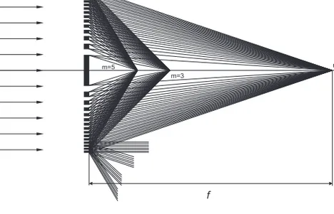
The main function of a zone plate is to diffract light so it interferes construc-tively at the focal point. This is accomplished by cancelling the destrucconstruc-tively interfering light with opaque zones or alternatively phase-shift the light by a factor of π. The symmetry of equal areas of every alternating zone pair (opaque/phase-shifting and transparent) is a prerequisite for a zone plate. Odd zones will be of a light enough material so X-rays can transmit through and even zones will be of a highly absorbing or phase-shifting material, or vice versa. A zone plate with opaque zones and with equally wide lines and spaces (line-to-space ratio = 1) diffracts the incoming light into different diffraction orders m as [18] ηm= ⎧ { ⎨ { ⎩ 0.25 m = 0 1/m2π2 m odd 0 m even
m=-1 m=0 m=3 m=1 m=-3 m=-5 l f m=5
Figure 3.1. Zone plate focusing into the first three odd diffraction orders. The
even diffraction orders are cancelled out for a zone plate with line-to-space ratio equal to 1. The focal length for the first diffraction order (m=1) is denoted f. Negative diffraction orders originate from virtual foci behind the zone plate. The first three negative orders and the transmission rays (m=0) are indicated for the outermost zones for clarity. Figure used with permission from A. Holmberg [36].
Figure 3.1 illustrates how the incoming light is diffracted into the different orders. Half of the incoming light is absorbed in the zone plate itself, 25% ends up in the 0th order and approximately 10% is diffracted in the 1st order. The latter number can for a given X-ray wavelength get as high as 40% for zone plates with a phase-shifting material (discussed in 3.2).
Only considering the first diffraction order, the squared radius of the nth zone is expressed as
r2
n=nλ(f + nλ4 )
where λ is the X-ray wavelength and f is the zone plate focal length. The larger the number of n is, the further out on the zone plate the zone is and the smaller its width (Figure 3.2). For zone plates, f is often larger than nλ 4 such that
rn≃ √
nλf
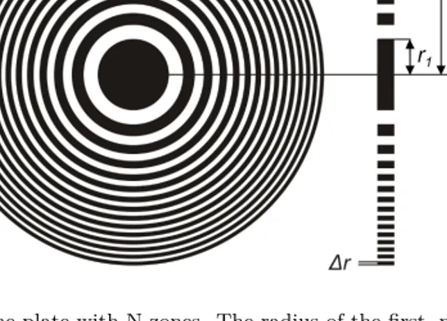
The total number of zones in a zone plate is denoted N, and the Nth zone is the outermost and the thinnest one. The radius of a zone plate with
Figure 3.2. Zone plate with N zones. The radius of the first, nth and outermost
zone N are denoted r1, rn and rN, respectively. The width of the nth zone is
drn and the outermost zone width is Δr. Figure used with permission from K.
Parfeniukas [37].
N zones will therefore be
rN≃ √
Nλf
The total number of zones, N, and the width of the outermost zone, Δr, are two important geometrical parameters involved in the focusing performance of a zone plate optic. In fact, the resolution of the zone plate optic is set by the width of the outermost zone
Δr ≃2rλf
N =
λ 2NA
where NA is the numerical aperture of the zone plate. A combination of these expressions shows that the number of zones in a zone plate is inversely square proportional to its resolution
N = r2N λf =
λf 4Δr2
From a fabrication point of view, this means that a doubling of the resolu-tion, i.e., halving the outermost zone width, will require the quadrupling of the number of zones. In some cases the diameter of the zone plate has to match the size of an incident beam. Then, the number of zones has to be adjusted accordingly. The smaller the outermost zone width, the better the zone plate resolution and hence the more challenging the fabrication.
So far, geometrical factors of the zone plate optic have been described. There are, however, certain restrictions the X-ray light source puts for the zone plate to reach its diffraction-limited performance. In the ideal case, a completely monochromatic light source should be used. Real sources have however an intrinsic spectral band width, Δλ, which has to be taken into account and restricts the maximum number of zones in a zone plate so that
Δλ
λ ≤
1 N
In order to get as good imaging performance as possible, the shift in focus caused by the source bandwidth Δλ should be less than the depth of focus, DOF, of the system
DOF = ± λ
2NA2
To summarize, the following parameters are taken into account when designing zone plate optics: the symmetry and equal area of alternating zone pairs, the intended X-ray wavelength of use (λ), the zone plate radius (rN), the number of zones (N) and the desired resolution, i.e., outermost zone width (Δr).
3.2 Zone plates for the hard X-ray range
Until now, this chapter has introduced zone plate properties mainly with respect to its geometry. When the X-ray wavelength and the design of the zone plate is decided upon it is time to find a zone plate material that gives the best focusing efficiency.
In the EUV and X-ray range, the complex refractive index is described as
n = 1 − δ + iβ
where δ and β are its real and imaginary components affecting the phase shift and absorption in the zone plate material, respectively. A higher first order diffraction efficiency than for zone plates with opaque zones is obtained by instead choosing a phase-shifting, partly transmitting material. This will reduce the absorptive photon losses. A phase shift of π will yield a maximum first order diffraction efficiency and the required thickness, or zone height, for a given wavelength and material is
t = λ 2δ
0 1 2 3 4 5 6 7 8 9 10 11 12 Zone height [µm] 0 5 10 15 20 25
Zone plate efficiency [%]
Figure 3.3. First order diffraction efficiency as function of zone height for
palla-dium, silicon and gold zone plates at 9 keV photon energy. Calculations were done in MATLAB using GD-Calc [38].
The zone plate first order diffraction efficiency takes into account both the real and imaginary parts of the refractive index and can be expressed as [29]
η = 1 π2(1 + e
−4πβt/λ−2e−2πβt/λ)cos(2πδt/λ)
The first order diffraction efficiency will reach its theoretical maximum by choosing a material with a β/δ ratio as small as possible and with a thickness giving a phase shift approaching π.
Figure 3.3 shows the variation of the first order diffraction efficiency with zone height of palladium, silicon and gold zone plates at 9 keV (0.14 nm). Palladium, silicon and gold zone plates reach their maximum theoretical efficiencies at zone heights of 2.5 μm, 11 μm and 1.8 μm, respectively. Even though their maximum theoretical efficiencies are lower than for silicon, palladium or gold would be suitable as zone plate materials for 9 keV use. Especially, their smaller zone heights, together with a small zone width for resolution, would be more feasible from a fabrication perspective. Instead, silicon that requires extreme aspect ratios at hard X-ray wavelengths, would be a good material to use as a mold for other, more opaque materials as palladium or gold.
This scenario is illustrated in Figure 3.4. Using silicon as a mold for these high-Z materials results in slightly lower theoretical first order diffraction efficiencies. A combined palladium/silicon zone plate reaches its maximum
0 1 2 3 4 5 6 7 8 9 10 11 12 Zone height [µm] 0 5 10 15 20 25 30 35 40
Zone plate efficiency [%]
Pd/Si Au/Si
Figure 3.4. First order diffraction efficiency as function of zone height for
com-bined palladium/silicon and gold/silicon zone plates at 9 keV photon energy. Cal-culations were done in MATLAB using GD-Calc [38].
focusing efficiency at 3.3 μm and a gold/silicon zone plate at 2 μm., i.e., at larger zone heights than pure palladium or gold zone plates. Both a lower first order diffraction efficiency and slightly thicker zones for a dual-material zone plate might seem unnecessary. However, using silicon as molds can provide mechanical stability to high-Z nanostructures. To conclude, it is not only the theoretical diffraction efficiency that is taken into account for the choice of zone plate material, but the availability in fabrication methods to manufacture high-aspect ratio, mechanically stable nanostructures.
3.3 Fabrication methods
Zone plate fabrication can be divided into two approaches: direct-write and etching processes. Independent of what approach is chosen for fabrication of the zone plate device, the first step in most modern zone plate fabrication methods is to define the pattern using electron beam lithography (EBL). EBL offers high resolution and good flexibility in the patterning process, and uses an electron sensitive polymer layer, or e-beam resist, in which the pattern is written. The following processing steps are then dependent on the intended X-ray wavelength of use and the desired aspect ratios.
zone plates that do not require as large zone heights as zone plates for hard X-ray wavelengths. There are two main methods that are included in the direct-write approach.
The first method uses a 1:1 line-to-space ratio zone plate design exposed in a positive resist, commonly poly(methyl methacrylate) (PMMA) [39]. In a positive resist the e-beam exposed polymer chains are fragmented into shorter fractions that are removed upon development. Electrodeposition (ED) is used to fill the mold with a high-Z and phase-shifting material, commonly gold or nickel [40]. Typically, silicon nitride membranes coated with a thin conductive plating base layer are used as substrates.
The second method uses a 1:3 line-to-space ratio zone plate design ex-posed in the negative, silicon-based resist hydrogen silsesquioxane (HSQ) [41]. In contrast to positive resists, the e-beam exposed chains in a negative resist are cross-linking and the unexposed resist is removed upon develop-ment. Larger zone heights can be obtained with HSQ than for a positive re-sist thanks to superior mechanical stability. Atomic layer deposition (ALD) is used to conformally coat the free-standing zones with a high-Z and phase-shifting material, e.g., iridium or platinum. Silicon nitride membranes are commonly used as substrates with this method.
The direct-write approach comes with the advantage of few processing steps and the disadvantage of small zone heights. One way to improve the zone thickness is to process both sides of the membrane [42] or stack multiple zone plates together [43, 44]. In both cases the alignment has to be very accurate and done with high precision [45].
3.3.2 Etching processes
Compared to the direct-writing approach, etching processes use thinner resist layers for the zone plate patterning. The EBL patterning becomes easier due to this, which is one of the advantages with the etching approach. Instead, the defined pattern is transferred into a substrate material. Etching processes for zone plate fabrication are categorised as reactive ion etching (RIE) and MACE.
RIE is a dry etching method that uses plasma for the pattern transfer. Here, an etch-resistant mask is used to selectively and anisotropically etch the substrate material that is not covered by the mask. The etched material is either a low-Z material that serves as mold for an electrodeposited high-Z
material, or a high-Z, phase-shifting material that is directly etched. Poly-imides are examples of a polymeric, low-Z materials that have served as zone plate mold for nickel ED [46], and tungsten and germanium are examples of materials that have been processed with RIE and used directly as a zone plate devices [47, 48]. In both cases, the material to be etched is deposited on a supportive substrate, commonly a silicon nitride membrane. Difficul-ties in nanostructure etching with a maintained vertical etching profile has led to limited possibility for improvement of the RIE process for zone plate fabrication. Instead, MACE has been shown to be a good alternative for fabrication of high-aspect ratio zone plate nanostructures with vertical etch profiles [49].
MACE is performed in both liquid-phase and gas-phase for zone plate fabrication [9]. Silicon is typically the substrate material used in MACE. After defining a 1:1 or 1:3 line-to-space ratio zone plate pattern in a posi-tive resist, a noble metal layer is deposited onto the silicon and the resist is removed in a lift-off process. The noble metal patterned silicon substrate is immersed in an etching solution or exposed to a gas-mixture consist-ing of hydrofluoric acid (HF) and an oxidant. The noble metal catalyzes the MACE reaction and anisotropically etches the silicon, transferring the zone plate pattern into the substrate. The 1:1 line-to-space ratio silicon zone plate mold is filled with a high-Z, phase-shifting material using ED or electroless deposition (ELD), typically gold or palladium [50]. The 1:3 line-to-space ratio structures are instead coated conformally using ALD, commonly with platinum [49,51].
MACE comes with the advantage and capability to fabricate high-aspect ratio nanostructures while maintaining etch verticality [52]. This makes this process attractive to various applications. MACE is a relatively new method for zone plate fabrication and the effect of the different process parameters on the resulting zone plate structures is unclear. This lends to the main goal of this thesis: to identify the most important etching parameters and investigate their influence on liquid-phase MACE of zone plate nanostructures.
Chapter 4
Metal-assisted chemical etching:
theoretical background
As introduced in the previous chapters, MACE opens up the possibility to fabricate high-aspect ratio zone plate nanostructures in silicon. The main method of focus in this thesis is liquid-phase MACE. To understand how dif-ferent experimental parameters involved in MACE will affect the zone plate etching, a description of the process theory is needed. In this chapter an overview of the etching process is introduced in 4.1; different mass transfer mechanisms are discussed in 4.2; the etching solution composition and the role of each component are in 4.3; the influence of the etching temperature is in 4.4; metal catalysts and their morphological effect on the etching are described in 4.5; and finally, influence of the silicon substrate properties are brought up in 4.6.
4.1 The etching process
Since its discovery in 2000 by Li and Bohn [13], MACE has been used for the fabrication of silicon-based nanostructures for a variety of applications. Advantages of the method are its relatively low cost, simplicity and ac-cessibility compared to other competing pattern transfer techniques. No sophisticated equipment is needed for the process and it can be performed in a chemistry laboratory. It was first introduced as a zone plate fabrica-tion method in 2014 by Chang and Sakdinawat [49] and has since then been employed not only for hard X-ray zone plates [50, 51, 53–57], but also for other diffractive X-ray optics [58,59].
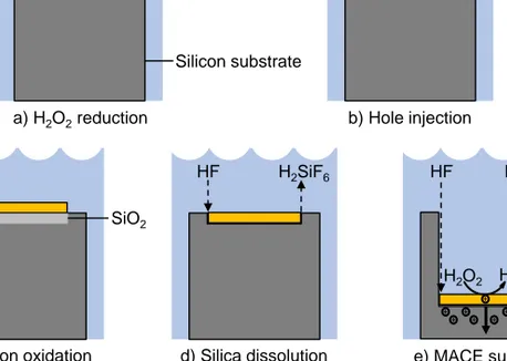
MACE is a mixed chemical and electroless etching process [60]. In a typical MACE experiment, a noble metal patterned silicon substrate is ex-posed to an etching solution consisting of HF and a strong oxidant. The
SiO2 c) Silicon oxidation a) H2O2reduction Silicon substrate Etching solution Noble metal H2O H2O2 HF H2SiF6
d) Silica dissolution e) MACE summary
b) Hole injection
H2O
H2O2
HF H2SiF6
Figure 4.1. Schematic illustration of the MACE process. a) The oxidant H2O2
is reduced at the noble metal surface and holes are formed as a result. b) The formed holes are injected into the silicon at the noble metal/silicon interface. c) The silicon is oxidized. d) The oxide layer is dissolved by HF. e) The steps in a)-d) are repeated and the noble metal catalyst is transferred into the silicon substrate.
silicon beneath the noble metal is typically etched much faster than the silicon without any noble metal coverage thanks to the catalytic activity of the metal. Without a noble metal catalyst, the etch rate of silicon is below 10 nm/h [61]. The morphology of the etched silicon is mainly defined by the morphology of the noble metal catalyst. For simplicity, the MACE process described in this section is based on the assumption that a silicon substrate patterned with an isolated noble metal catalyst layer is etched in an etching solution composed of HF and the oxidant hydrogen peroxide (H2O2).
In the MACE process, there is a cathode site (noble metal surface) and an anode site (silicon surface) with local hole currents flowing between them. The H2O2 is reduced at the noble metal catalyst surface as follows
H2O2+2H+→2H2O + 2h+
This cathode reaction is well accepted as the first step in the MACE process. The generated holes are injected into the silicon substrate at the noble
2 2
The balanced redox reaction at the noble metal/silicon interface is Si + 2H2O2→SiO2+2H2O
Following the hole injection and oxidation of silicon, the formed silica is dissolved by HF
SiO2+6HF → H2SiF6+2H2O
A combination of the redox reaction and the silica dissolution reaction gives the following overall MACE reaction
Si + 2H2O2+6HF → H2SiF6+4H2O
Other proposed anode reaction mechanisms include direct dissolution of silicon. The mechanism proposed for direct dissolution of silicon in tetrava-lent state is [13,64]
Si + 4h++4HF → SiF
4+4H+ SiF4+2HF → H2SiF6 and a proposed general mechanism is [60]
Si + nh++6HF → H
2SiF6+nH++4 − n2 H2
with n ranging from 2 to 4. Taking the cathode reaction into account, the overall MACE reaction can be expressed as
Si + n2H2O2+6HF → H2SiF6+nH2O +4 − n2 H2
To summarize, there is no established MACE reaction mechanism due to difficulties in analyzing the surface state of silicon in-situ. Ex-situ anal-ysis will be uncertain due to the formation of native oxide on silicon in the atmosphere. Today, the generally accepted MACE process is: (1) The ox-idant is predominantly reduced at the surface of the noble metal catalyst and holes are formed. (2) The holes diffuse through the noble metal layer and are injected into the silicon. The hole concentration is largest at the
noble metal/silicon interface. (3) The silicon is oxidized upon injection of holes. (4) The oxidized silicon is dissolved by HF and the byproducts re-sulting from the dissolution are transferred from the reaction site. There are different models proposed on how the mass-transport to and from the reaction site is taking place.
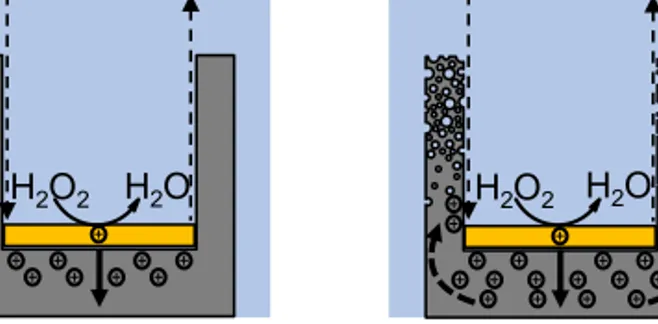
4.2 Mass-transport models
There are three models proposed for the transport of reagents to and byproducts from the MACE reaction site, as illustrated in Figure 4.2. Model I and Model II suggest a mass-transport occurring at the noble metal/silicon interface, while Model III proposes that the etching occurs at the noble metal surface.
In Model I, the catalyst is continuous and the transport of reagents and byproducts occurs along the metal/silicon boundaries [61]. The reagent/byproduct diffusion length is mainly determined by the lateral size of the catalyst layer. The larger the catalyst pattern, the slower the etching due to limited diffusion and vice versa.
In Model II, the catalyst is porous and the transport of the reagents and byproducts occurs through the pores in the metal [65]. In contrast to Model I, the reagent/byproduct diffusion length in Model II is determined by the thickness of the catalyst layer. Hence, the thicker the catalyst layer the slower the etching due to slower diffusion and vice versa.
In Model III, silicon atoms diffuse through the catalyst layer to the catalyst surface [16]. The basis for this proposal is the tendency of silicon to mix into metals by diffusion [66, 67]. While at the surface of the noble metal, the silicon atoms are oxidized and further dissolved. According to this model, the etching rate is determined by the thickness of the catalyst layer.
Studies have been conducted to identify how the mass-transport oc-curs [61, 68]. The difficulties in in-situ and ex-situ analyses limit the clas-sification of the mass-transport model. MACE occurs both with a thick, continuous metal catalyst with no pores and with thin, porous metal cata-lysts. Thus, pores in the metal catalyst is not a perquisite for the MACE reaction (oxidation and dissolution of silicon) to occur, but facilitates the mass-transport especially for catalysts in the microscale [69].
4.3 Etching solution
In section 4.1 the MACE process was introduced based on an etching so-lution with H2O2 as the oxidant. An etching solution consisting of H2O2 and HF is by far the most frequently reported composition used in MACE.
Model I
HF H2SiF6
Model II
Model III
Silicon atoms
Figure 4.2. Schematic illustration of the three proposed models for mass
trans-port during MACE. In Model I, the reagents and byproducts diffuse along the noble metal/silicon interface. In Model II, the reagents and byproducts diffuse through pores in the noble metal catalyst. In Model III, silicon atoms from the substrate diffuse through the noble metal catalyst and gets oxidized and dissolved on the noble metal surface.
Also, it is the etching solution composition used in this thesis. It is however worth mentioning that other oxidants are used as well, e.g., nitric acid and metal salts [70].
The concentrations of H2O2 and HF affect both the etch rate and the morphology of the etched structures. It is suggested that the hole injection rate is controlled by the concentration of H2O2 while the HF concentra-tion regulates the silicon dissoluconcentra-tion rate [16]. A balance between the hole injection and dissolution rates will, based on this, result in the metal cat-alyst pattern being transferred into the silicon without any morphological changes. When the hole injection rate is faster than the dissolution rate, i.e., concentration of H2O2 too high, a surplus of holes are present at the
noble metal/silicon interface. These holes can diffuse away in an uncon-trolled manner, oxidize and subsequently etch other sites on the silicon, as illustrated in Figure 4.3. This introduces a certain degree of porosity to the surrounding silicon structures [54].
Alcohol additives in the etching solution do not take part in the etching reaction but influence the etching outcome. The effect of isopropanol (IPA) has shown to reduce the etch rate, improve the etching uniformity over large catalyst areas and reduce porosity formed as a consequence of off-site etching [59, 71]. Furthermore, large concentrations of alcohol additives influence the curvature of etched silicon nanostructures [72,73].
H2O H2O2 HF H2SiF6 a) H2O H2O2 HF H2SiF6 b)
Figure 4.3. Schematic illustration of the hole injection rate a) in balance with
the silicon dissolution rate resulting in hole consumption at the noble metal/silicon interface, and b) higher than the hole consumption rate at the noble metal/sili-con interface resulting in holes diffusing to other sites of the silimetal/sili-con followed by oxidation and dissolution of those sites.
4.4 Temperature
The etching temperature is believed to have a similar effect on the MACE reaction kinetics as the concentration of the etching solution. The overall etch rate (oxidation and dissolution) will increase with temperature due to the provided energy to the system and result in deeper transfer of the noble metal catalyst pattern into the silicon substrate [16,74,75]. The increase in temperature also comes with the side effect of an off-site etching, similarly to the effect of the oxidation rate described in 4.3 [54,75].
4.5 Metal catalysts
Noble metals are used in MACE for fabrication of structures with defined morphology. The reason for this is their ability to preserve their structures without dissolving in the etching solution. Commonly used noble metals
of the etched structures. For defined patterns in the nanoscale, EBL is combined with electron beam evaporation for deposition of the catalyst. Other methods include nanosphere lithography combined with evaporation to form close-packed dot arrays and ELD of a metal precursor to form nanoparticles, dendrites and continuous or discontinuous films [70].
MACE of lithographically defined catalyst patterns often needs to be controlled and follow a defined etching direction. Vertical etching is for in-stance of high importance for zone plate fabrication. Etching verticality is favored by an interconnected catalyst pattern providing a collective etching into the silicon substrate. Isolated catalysts, especially in the nanoscale, tend to etch in an uncontrolled manner due to their freedom of movement. Substrate surface defects or facets in the catalyst tend to have a bigger im-pact on the course of the etching of catalysts in the nanoscale than catalysts in the microscale.
a)
a) b) c)
200 nm 200 nm
5 μm
Figure 4.4. Scanning electron microscopy (SEM) micrographs of different
cata-lyst morphologies. Light parts are gold and dark parts are silicon. a) KTH Royal Institute of Technology logo defined with EBL. b) Dot array defined by nanosphere lithography. c) Nanoparticles.
4.6 Silicon
Among all conditions involved in MACE, the silicon doping type has shown a minor effect on the etching outcome [70]. The etching process is in other words independent of if the substrate is p- or n-type. On the other hand,
the doping concentration is critical and shows a great influence on the etch morphology. The higher the doping concentration of the starting silicon substrate, the greater the post-etch porosity degree and surface roughness [76–79].
Generally in MACE, at low etch rates the preferential anisotropic etch trend is vertical along the <100> direction irrespective of the substrate crystal orientation [16, 70]. According to the back-bond strength theory, a weakening of the silicon back-bonds in the <100> is stronger than it is for other directions since there is the lowest density of back-bonds to be broken [63]. The effective back-bond number density increases with (100)<(110)<(111) [9]. As a consequence, less energy is required to etch the silicon along the <100> direction. However, etching along non-<100> directions have been reported at extremely high etch rates, suggesting a correlation between the etch rate and direction [73,80]. Breaking of higher density back-bonds can thus be kinetically favored at sufficiently high etch rates.
Summary
In this chapter the fundamentals of MACE have been explored. Different theories on how the etching occurs have been presented and the effects of etching solution composition, temperature, metal catalyst and properties of the silicon substrate have been discussed. These topics will serve as a basis for later discussions on the influence of MACE parameters on zone plate etching in Chapter 6. Before that, the overall fabrication process of zone plate devices will be presented in Chapter 5.
Chapter 5
Nanofabrication of silicon-based
zone plates
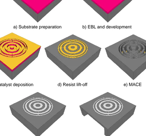
In this chapter, all steps for the fabrication of silicon-based zone plates are presented. The described process starts with a silicon substrate and ends with a zone plate device ready to be used in a hard X-ray nanoprobe setup. The overall zone plate fabrication method involves four main parts: (1) Zone plate design, patterning by e-beam lithography and gold deposition onto silicon, (2) pattern transfer via MACE into substrate to form a zone plate mold, (3) metalization of the mold, and (4) back-thinning of substrate. Each part has its own set of parameters and considerations that are thoroughly analyzed in its respective section. The main points of this chapter formed the basis for the work presented in Paper C.
5.1 Zone plate design, patterning and deposition in gold
The first part of the zone plate device fabrication is illustrated in Figure 5.1 a)-d) and prepares the substrate for MACE. When designing zone plates for fabrication with MACE, etching verticality and mechanical stability has to be taken into account. The etching gets more homogeneous when the zones in the catalyst pattern are interconnected. On the contrary, breaks in the zones of the catalyst pattern instead result in connections in the silicon and contribute with mechanical stability to the zone plate mold. Connects between the metal catalyst zones are called ”positive supports”, whereas breaks in the metal catalyst zones are called ”negative supports” (shown in Figure 5.2). Different investigated designs and their influence on the MACE outcome are discussed in Chapter 6. The zone plates were designed using the Raith_GDSII MATLAB toolbox that generates patterns compatible with Raith EBL systems [81].
c) Catalyst deposition d) Resist lift-off e) MACE a) Substrate preparation b) EBL and development
f) Metallization g) Substrate back-thinning
Figure 5.1. Overview of the zone plate nanofabrication process. a) Silicon
substrate (dark grey) preparation by spin-coating 80 nm CSAR 62 e-beam resist (pink). b) Zone plate patterning by EBL and development for removal of resist residues. c) Deposition of 2 nm titanium and 10 nm gold (yellow) by evaporation. d) Lift-off of resist layer leaving the metal zone plate pattern only. e) Transferring the metal zone plate pattern into the substrate via MACE. f) Metallizing (light grey) the silicon mold via ELD or ED. g) Back-thinning the substrate via RIE. Figure adapted from Paper C.
The methacrylate-based e-beam resist CSAR 62 from Allresist GmbH was mainly used in this thesis. A thickness of 80 nm was typically spin coated on clean 1.5 cm x 1.5 cm silicon substrates. The size of the substrates were chosen to provide a large enough area with an even resist thickness for the zone plates to be exposed, as well as for easy handling throughout the fabrication process. The resist spin-coating was followed by 60 s baking on a 180∘C hot plate. Thanks to the high sensitivity of CSAR 62 [82] and the
1 μm
Figure 5.2. SEM micrographs of innermost parts of zone plates picturing a)
positive and b) negative supports, respectively. Same scale bar applies to both micrographs.
50 μm
Figure 5.3. Zone plate design in gold on silicon. The gold acts as the catalyst
in a later MACE step. The zone plate design diameter is 150 μm and outermost zone width is 30 nm.
high electron current of the used 50 kV Raith Voyager system, each zone plate with a 150 μm diameter, 1:1 line-to-space ratio and 30 nm outermost zone width took in average 3 min to expose. A zone plate pattern with such dimensions is pictured in Figure 5.3. An observation on the CSAR 62 resist is its tendency to leave residues in the pattern after development in amyl
acetate, even with a clearance dose. A short, 13 s oxygen plasma ashing step was therefore found necessary to remove all the remaining resist in the exposed areas for proper metal adhesion to the silicon substrate.
Gold was used as the MACE catalyst throughout this work. The metal deposition was performed using a custom in-house Eurovac/Thermionics electron-beam evaporator. Since gold does not adhere directly to the oxide layer present on the silicon substrate surface, an adhesive 2 nm titanium film was evaporated at 1 Å/s right before the gold deposition. It should be noted that the titanium layer immediately dissolves in HF when exposed to the etching solution and does not take part in the MACE process [83]. A gold thickness of 10 nm was chosen and evaporated at 2 Å/s. The choice on the gold thickness was based on a few considerations. Firstly, the thinner the resist layer the easier the resist lift-off, especially in the outermost parts of the zone plate pattern where the zones are as small as 30 nm. Secondly, a thicker gold film would require a thicker resist layer, too. If the gold film is too thick in relation to the resist thickness, the deposited gold will connect to gold on top of the resist forming bridges and the lift-off will fail. The resist thickness affects the stability of the pattern, especially in the outermost parts of the zone plate pattern. When the resist got thicker than 80 nm, the smallest exposed features tended to collapse after development, as is shown in Figure 5.4. Lastly, a gold thickness of 10 nm is within the range of previously reported catalyst thicknesses for optics fabrication [49,51].
b)
500 nm c)
a)
Figure 5.4. SEM micrographs gold zone plate patterns (outermost parts) after
CSAR 62 lift-off with thicknesses a) 80 nm, b) 130 nm and c) 200 nm. The scale bar applies to all three micrographs.
The resist lift-off was performed in dimethyl succinate and included sev-eral sequences of high power ultrasonication. Before the actual lift-off, some preparatory steps were found to be especially important for a successful pro-cess. Directly after the metal deposition, the substrates were left to soak in dimethyl succinate for at least 12 hours. Right before the
ultrasonica-transferred to isopropanol and thereafter to deionized water (DI H2O) and ultrasonicated for an additional 10 min in each solvent. The total time required for the entire lift-off process was approximately one hour.
5.2 Pattern transfer with metal-assisted chemical etching
This section describes the practicalities of a typical MACE process used in this thesis (Figure 5.1 e)). The investigation of different experimental parameters and their effect on the etching outcome is presented in Chapter 6. Silicon wafers of p-type (100) with boron doping and resistivity of 1–5 Ω·cm were used for the most part throughout this work. The thickness of the wafers was 250 μm. For the study of silicon doping effect on zone plate etching p-type (100), boron doped wafers with a resistivity of 0.001-0.005 Ω·cm were additionally used. The latter silicon-type was further used for the proof of concept of ED metalization.
The MACE reaction is initiated on the surface of the gold catalyst (Chapter 4). Therefore, it is of high significance that the substrate surface, and especially the gold surface, is free from adsorbed organics and other impurities that might prevent the etching from starting. A 3 min oxygen plasma cleaning step was introduced right before the MACE to ensure a reproducible process.
A typical etching solution consisted of HF, H2O2 and DI H2O and was freshly prepared before each experiment. The MACE was performed in a polytetrafluoroethylene container under light protection to exclude any in-fluence from surrounding illumination [84]. All experiments were conducted using an etching solution volume of 15 ml to ensure the abundance of reac-tants. The clean substrates were mounted on the bottom of the container to prevent any movement that might disrupt the etching. When the influ-ence of temperature on the etching was assessed, pre-temperature regulated chemicals were used to prepare the etching solution and the MACE was performed using a Lauda Eco RE620 Silver thermostat and bath for tem-perature control. The etching was initiated after temtem-perature stabilization of both the substrate and the etching solution. Every investigated MACE condition was repeated at least three times.
After MACE, the substrates were rinsed in copious amounts of DI H2O and transferred to ethanol. The samples were critical point dried over 20
5 μm a) 5 μm b) 1 μm c) 4 μm d) 4 μm e)
Figure 5.5. SEM micrographs of gold patterned silicon pre- and post-MACE.
KTH logo a) pre-MACE and b) post-MACE. c) pictures the inset in b) where the difference in the MACE outcome of smaller and larger structures is clear. The smallest circular details in the KTH crown show a broader tendency to collapse compared to the larger circles. An interconnected zone plate pattern with positive supports is shown in d) pre-MACE and e) post-MACE. Adapted from Paper B.
cycles using a Leica EM CPD300. Figure 5.5 pictures examples of MACE processed patterns.
5.3 Metalization methods
Until now, the nanofabrication of silicon zone plate molds has been de-scribed. As explained in Chapter 3, the use of high-Z materials is advan-tageous from a fabrication point of view for the zone plates to function at hard X-ray wavelengths. In this section, two different plating methods to metallize silicon zone plate molds with palladium and gold are presented (Figure 5.1 f)).
and deposited metal now acts as a catalyst in the process and the metal buildup continues on the same site. For the metalization of silicon molds, a selective deposition on the gold at the bottom of the etched zone plate struc-tures is desired. Therefore, as a preparatory step, a 3 min oxygen plasma treatment was performed to passivate the silicon surface by oxidation. This way, any palladium deposition on other sites than the catalytic gold layer was prevented (see Figure 5.6). The plasma treatment also added to the hydrophilic character and thus easier wetting of the gold surface. Contact angle measurements revealed a change from 89∘ to 29∘ due to adsorbed oxygen or presence of an oxide layer on the gold surface [87,88].
The PD-Tech PC electroless Pd system from Atotech was used for the palladium deposition. A fresh 100 ml plating bath was prepared for each sample to ensure process reliability and the plating was performed under magnetic stirring at 120 rpm. Inductively coupled plasma optical emission spectrometry (ICP-OES) measurements revealed a palladium concentration of 5 mM per plating bath. The plating temperature was set to 40∘C and the process was initiated when immersing the substrate into the plating bath. In early plating experiments, the substrates were sitting vertically in
50 μm
Figure 5.6. SEM micrograph of ELD metallized palladium/silicon zone plate.
The palladium is selectively deposited in the zone plate area. Figure adapted from Paper C.
300 μm a)
200 μm b)
Figure 5.7. SEM micrographs of palladium plated zone plates using different
setups. In a) the substrate was sitting in a holder at the bottom of the plating bath. The zone plates are not plated, completely plated and semi-plated in the top, middle and bottom row, respectively. In b) the substrate was immersed into the bath from the top which resulted in homogeneous plating of all zone plates.
a holder at the bottom of the plating bath. This experimental setup resulted in uneven plating over single zone plates and complete or no plating of zone plates on the same substrate. Instead, the setup was changed so that the substrates were immersed into the plating bath from the top which resulted in a more homogeneous plating, as pictured in Figure 5.7.
For a zone plate to reach its maximum theoretical efficiency, the den-sity of the zone plate material should be close to the tabulated denden-sity of the material. The tabulated density value for palladium is 12 g/cm3. The density was assessed from plated films by gravimetric analysis and trans-mission measurements. Samples were prepared similarly to the zone plates, but instead a predefined area of 1.5 cm x 1.5 cm plating base (2 nm tita-nium adhesion layer and 10 nm gold) on silicon substrates were plated. The gravimetric analysis was performed by measuring the weight of the plated
ence points on the same chip. Relating the thickness of the films to the transmitted photons, the density of the palladium films were calculated. The average density calculated from transmission data of three plated films were 10.9 ± 0.2 g/cm3. Both measurements show a lower palladium den-sity than the theoretical value. The incorporation of relatively light-weight elements in the bath formulation, such as brighteners, and the presence of pores or voids in the plated metal would be reasons for this [89]. Figure 5.8 pictures a palladium metallized zone plate. The efficiency characterization of these palladium/silicon zone plates is presented in Chapter 7.
500 nm
Figure 5.8. SEM micrograph showing the innermost part of a partly palladium
plated silicon zone plate.
5.3.2 Gold electrodeposition
Another way to selectively metallize the zone plate mold is through ED [90]. The essential components in the ED process are a cathode, an anode or counter electrode and the plating solution that holds the metal complex to be plated in a stable and reducible form [91]. A current is applied to the cathode, in this case the substrate holding the zone plate molds, which attracts the surrounding metal complexes. Upon polarization of the metal complex in the electric field, the ligand gets stripped off and the metal gets deposited on the charged cathode surface [89]. The silicon surface was passivated through a 3 min oxygen plasma treatment to avoid any deposition off-site the zone plate structures. The ED was performed at 50∘C in a 8 ml plating bath based on gold sulphite from Schütz Dental GmbH. From ICP-OES measurements the gold content in the bath was determined to be
70 mM. In Figure 5.9 we demonstrate the proof of concept of selective gold ED of a MACE processed zone plate.
2 μm a)
500 nm b)
Figure 5.9. SEM micrographs of gold plated zone plate. The plating time was 1
min and the applied current 15 μA. b) shows a magnification of the inset area in a).
5.4 Substrate back-thinning
The zone plate substrate needs to be more or less transparent to the in-coming X-rays. A 250 μm thick silicon substrate, as used in this work, only transmits 7.8 % of 9 keV light. While a thick substrate is robust and easy to handle, it requires thinning down to be used as a device. Furthermore, the thinned-down substrate needs to have a uniform thickness over the zone plate area to ensure the same phase-shift throughout the entire zone plate. The silicon substrate back-thinning makes the final part of the zone plate nanofabrication process (Figure 5.1 g)).
For this, a two-step deep reactive ion etching (DRIE) was used [92]. As a preparation, the positive photoresist Microposit S1813 was spin-coated on both the back of the silicon chip and the zone plate front for protection. Using the Smartprint optical maskless lithography system, circular sites at the back parts of the zone plates were defined and the photoresist was de-veloped for 60 s in Microposit MF-319 developer. Chromium was deposited by thermal evaporation to act as an etch mask during the DRIE and the resist was removed in a lift-off process in acetone under sonication.
The first step was a cryogenic DRIE step at -50∘C followed by a second short DRIE step at 30∘C for polishing purposes. The etching was performed in a gas mixture of sulfur hexafluoride (SF6), oxygen (O2) and fluoroform (CHF3) [93]. An etch rate of 9 μm/min was obtained with this process. Figure 5.10 shows a cross-section of a thinned down and polished substrate.
50 μm
Figure 5.10. SEM micrograph of a thinned down silicon substrate cross-section
prepared with the presented DRIE process. Figure adapted with permission from F. Lundberg [92].
Chapter 6
Optimization of metal-assisted
chemical etching for zone plate
nanostructures
With MACE as the pattern transfer method, hard X-ray zone plate optics fabrication has taken a new turn. Since the first study in 2014 [49], the number of publications has rapidly increased [9]. The reasons for the interest in MACE for hard X-ray optics fabrication is the capability of the method to fabricate ultra-high aspect ratio silicon nanostructures while being relatively simple and low-cost [15,52].
High-aspect ratio silicon structures are desired for both resolution and focusing efficiency purposes. For fabrication of a good quality zone plate, there are important morphological characteristics that need to be main-tained during MACE. In order to diffract the photons into the correct orders with high efficiency, the etched silicon zones must be vertical and mechan-ically stable. This is especially important for a successful metalization of the silicon mold in a later fabrication step. Another important morpholog-ical aspect is the surface of the zone sidewalls. The walls must be dense and smooth to avoid any focusing efficiency loss and to obtain the aimed resolution of the device [94].
Based on the morphological characteristics mentioned above, this chapter describes the experimental investigation about the influence of the MACE parameters presented in Chapter 4 on zone plate etching. The effect of etching solution and temperature on the reaction kinetics is discussed, different zone plate designs are studied in terms of etching verticality and mechanical stability of the silicon nanostructures and the effect of silicon resistivity on silicon wall roughness is shown. Papers A, B and D were mainly based on the work presented in this chapter.
6.1 Etching solution composition
At relatively high HF concentrations, the oxidant in the etching solution is the MACE rate determining reactant [60]. We investigated the kinetic and morphological effects of the oxidant H2O2 by systematically increas-ing its concentration while keepincreas-ing the HF concentration constant. The experimental parameters for this study are listed in Table 6.1.
Table 6.1. Investigated MACE conditions for the study of etching solution
compo-sition influence on zone plate etching. The HF concentration ([HF]), temperature (T), etch time (t), outermost zone width (Δr) and silicon resistivity (ρSi) were kept constant. An etching time series was performed with the etching solution composition containing 0.68 M H2O2. [H2O2] : [HF] (M) T (∘C) t (min) Δr (nm) ρSi (Ω·cm) 0.17 : 4.7 25 4 100 1-5 0.34 : 4.7 25 4 100 1-5 0.68 : 4.7 25 4, 8, 16, 32 100 1-5 1.4 : 4.7 25 4 100 1-5
As pictured in Figure 6.1 a)-c), dense and smooth silicon zones were obtained up to a H2O2 concentration of 0.68 M. The investigated H2O2 concentrations up to this point gave a linear etch trend where 0.17 M, 0.34 M, 0.68 M resulted in ≈0.70 μm, ≈1.3 μm and ≈2.6 μm etch depths, respec-tively. This trend did not continue at the highest studied H2O2 concentra-tion of 1.4 M. At this concentraconcentra-tion, the zones appeared rough, indicating porosity, and the etch depth was only ≈0.87 μm (Figure 6.1 d)). A compar-ative atomic force microscopy (AFM) study using a Bruker FastScan system in tapping mode showed that the surface roughness of the third zone at 0.68 M H2O2 and 1.4 M H2O2 were 0.56 nm rms and 2.3 nm rms, respectively.
a)
2μm 1 μm
b) c) d)
Figure 6.1. Effect of etching solution composition. Zone plates etched at H2O2
concentrations of a) 0.17 M, b) 0.34 M, c) 0.68 M and d) 1.4 M and a constant HF concentration of 4.7 M. Same scale bars apply to main SEM micrographs and the insets. The insets show the outermost zones. Figure adapted from Paper A.
tion rate, all holes are consumed at the gold/silicon interface and the etching behaviour is linear. When, however, the hole injection rate is faster than the silicon dissolution a surplus of unconsumed holes can diffuse into the silicon zones and result in a randomized etching behaviour. This effect might be enhanced by our interconnected zone plate design with positive supports, where every silicon pillar is surrounded by the gold catalyst which to a larger extent might contribute to off-site etching. Since the etching solution with 0.68 M H2O2 gave the most profound etch depth with maintained dense and smooth zone walls, it was used for further investigations of achievable etch depths in a time study.
The optimized etching solution composition together with an intercon-nected zone plate catalyst design were seemingly not limiting in terms of achievable etch depths (see Figure 6.2). The etching trend was linear (≈0.7 μm/min) indicating an abundance of chemicals in the etching solution with an effective replenishment of reactants at the catalytic sites. The pH value
1 μm
5 μm
Figure 6.2. Zone plate etch depth as a function of etch time, based on
cross-section SEM micrograph analysis. The error bars represent the standard deviation of etch depth measurements along the zone plate profile. The MACE processing was performed with an etching solution containing 0.68 M H2O2. The top-left
inset shows zone plate structures etched for 4 min. The cross-section was made by focused ion beam (FIB) milling. The bottom-right inset shows zone plate structures etched for 16 min. The cross-section was prepared by manual cleaving. Figure from Paper A.
was maintained throughout the whole time study showing that the con-sumption of HF in the MACE process was negligible with respect to the large etching solution volume (pH= 0–0.5). A vertical etching direction was maintained with the interconnected zone plate catalyst design, however as the bottom-right inset in Figure 6.2 depicts, collapse of zones became an issue at large etch depths due to free-standing silicon pillars. The silicon zone plate structures were stable up to 8 min etching at an etch depth of ≈6 μm. The effect of different zone plate designs is further explored in 6.3.
6.2 Processing temperature
To understand how the MACE processing temperature affects the reaction kinetics and morphology of silicon structures, the influence of the etching solution temperature was investigated. For this, the etching solution with 0.68 M H2O2was used. The experimental details for the temperature study are listed in Table 6.2.
Table 6.2. Investigated MACE conditions for the study of processing temperature
influence on zone plate etching. The etching solution composition ([H2O2] : [HF]),
etch time (t), outermost zone width (Δr) and silicon resistivity (ρSi) were kept
constant. T (∘C) [H 2O2] : [HF] (M) t (min) Δr (nm) ρSi (Ω·cm) 10 0.68 : 4.7 4 100 1-5 25 0.68 : 4.7 4 100 1-5 40 0.68 : 4.7 4 100 1-5
Figure 6.3 a) shows that etching at 10 ∘C, which was the lowest inves-tigated temperature, resulted in the smallest etch depth (≈0.32 μm). This can be attributed to slower hole injection and silicon dissolution rates at lower temperatures. As presented in the previous section, room temper-ature processing resulted in considerably deeper etching (≈2.6 μm, Figure 6.3 b)). Etching at 40∘C, the highest temperature studied, did not result in a larger etch depth than room temperature processing (≈1.2 μm, Figure 6.3 c)). In addition, the silicon structures had a rough appearance and AFM measurements revealed a surface roughness of 3.8 nm rms (0.56 nm rms at room temperature etching). This suggests that the hole injection and consumption reaction kinetics are out of balance and a diffusion of surplus holes to the surrounding silicon pillars.
![Figure 2.1. Layout of the NanoMAX beamline and its two hard X-ray nanoprobes [34].](https://thumb-eu.123doks.com/thumbv2/5dokorg/5466121.142108/16.892.200.685.773.965/figure-layout-nanomax-beamline-hard-x-ray-nanoprobes.webp)