Technical Report, IDE0747, May 2007
Low Noise Amplifier for Radio Telescope at 1.42 GHz
Master’s Thesis in Electrical
Engineering
Venkat Ramana. Aitha, Mohammad Kawsar Imam
Supervisor: Emil Nilsson
School of Information Science, Computer and Electrical Engineering Halmstad University
Low Noise Amplifier for Radio Telescope at 1.42 GHz
Master’s Thesis in Electrical Engineering
School of Information Science, Computer and Electrical Engineering
Halmstad University
Box 823, S-301 18 Halmstad, Sweden
May, 2007
Preface
This Master’s thesis in Electrical Engineering has been conducted at the School of Information Science, Computer and Electrical Engineering at Halmstad University. This is a part of the research project “Radio telescope system” working at 1.42 GHz. We realized that it would be hard to finish the project in time, but with all the kind help from the persons that are to be mentioned, we managed to carry the project to a conclusion within time. First of all we would like to thank Emil Nilsson and Professor Arne Sikö for providing us an opportunity to work on this project under their supervision and guiding us throughout the project. We would also like to thank Ruben Rydberg for his great help and advice throughout the project.
We are also very grateful to Jörgen Carlsson for his cooperation at every phase of our project. We would also like to give special thanks to Christopher Allen for correction, comments and proofreading of our thesis from an English point of view. Further, we are particularly very grateful to our parents who always supported and encouraged us during our stay and study in Sweden.
Venkat Ramana.Aitha & Mohammad Kawsar Imam Halmstad University, May 2007.
Abstract
This is a part of the project “Radio telescope system” working at 1.42 GHz, which includes designing of patch antenna and LNA. The main objective of this thesis is to design a two stage low noise amplifier for a radio telescope system, working at the frequency 1.42 GHz. Finally our aim is to design a two stage LNA, match, connect and test together with patch antenna to reduce the system complexity and signal loss.
The requirements to design a two stage low noise amplifier (LNA) were well studied, topics including RF basic theory, layout and fabrication of RF circuits. A number of tools are available to design and simulate low noise amplifiers but our simulation work was done using advanced design system (ADS 2004 A).
The design process includes selection of a proper device, stability check of the device, biasing, designing of matching networks and layout of total design and fabrication. A lot of time has been spent on designing of impedance matching network, fabrication and testing of the design circuits and finally a two stage low noise amplifier (LNA) was designed. After the fabrication work, the circuits were tested by the spectrum analyzer in between 9 KHz to 25 GHz frequency range. Finally the resulting noise figure 0.299 dB and gain 24.25 dB are obtained from the simulation. While measuring the values from the fabricated circuit board, we found that bias point is not stable due to self oscillations in the amplifier stages at lower frequencies like 149 MHz for first stage and 355 MHz for second stage.
Tables of Contents
1 Introduction………....1
1.1 Background ………...1
1.2 Purpose and Motivation……….2
1.3 Target Specification……….. 3 1.4 Outline of Thesis………... 3 2 Related work………..5 3 Theoretical Background………...… 7 3.1 Introduction of LNA……….……… 7 3.2 LNA Architectures……….…...7 3.2.1 Resistive Termination………...………7 3.2.2 1/gm Termination………..9
3.2.3 Shunt Series Feedback ……….9
3.2.4 Inductive Degeneration………10
3.3 RF Basic Concepts………10
3.3.1 Noise Figure……… 10
3.3.1.1 Noise Figure of Cascading Stages………11
3.3.2 Scattering Parameters……… 11
3.3.2.1 Definition of Scattering Parameters………12
3.3.3 Stability………14
3.3.3.1 Stability Techniques……….14
3.3.4 Transistor Biasing………14
3.3.4.1 Fixed Biasing ………..15
3.3.4.2 Collector to Base Bias ……….16
3.3.4.3 Voltage Divider Bias ………...17
3.3.5 Smith Chart………..19
3.3.6 Impedance Matching………22
3.3.7 Gain………..26
3.3.7.1 Transducer Power Gain………...26
3.3.7.2 Operating Power Gain………26
3.3.7.3 Available Power Gain……….………....26
3.3.7.4 Maximum Unilateral Transducer Power Gain……… 27
3.3.7.5 Maximum Transducer Power Gain……….……… 27
3.3.7.6 Maximum Stability Gain……….…… 27
4 LNA Design Process………..…… 29
4.1Transistor Selection……… 29
4.2 Checking the Stability……… 29
4.4 Layout of LNA………37
4.4.1 Simulation Result of Final Layout with real components………..38
4.5 Comparing Results………...41
5 Fabrication and Test plan ………...……… 43
5.1 Fabrication ………..…… 43
5.2 Test Plan………43
6 Conclusion and Future Work……… 47
7 Appendix ………. 49
8 Abbreviations………... 59
9 References...……….. 61
List of Figures
Figure 1 Block Diagram of a Typical Radio Receiver 2
Figure 2 Resistive Termination 8
Figure 3 1/gm Terminations 9
Figure 4 Shunt-series Feedback 9
Figure 5 Inductive Degeneration 10
Figure 6 Cascaded Noisy Stages 11
Figure 7 Two Port Networks 12
Figure 8 Fixed Bias 15
Figure 9 Collector to Base Bias 16
Figure 10 Voltage Divider Bias 17
Figure 11 Voltage Divider Circuits 18
Figure 12 The Smith Chart 19
Figure 13 Constant Resistance Circles 20
Figure 14 Constant Reactance Circles 20
Figure 15 Combination of Z and Y Smith Chart 21
Figure 16 Circuit 22
Figure 17 Power Graph 23
Figure 18 Showing the Basic Diagram of Matching 24 Network for one Device
Figure 19 (a to d) Examples of Matching Circuit 24 to 26 Figure 20 Stability Circuit with Ideal Components 30
Figure 21 DC Bias setup for Two Transistors 30
Figure 22 DC Bias Curves for Two Transistors 31
Figure 23 Bias Networks with Ideal Components for Two Stage LNA 32
Figure 24 Input Matching 32
Figure 25 Intermediate Matching 33
Figure 26 Output Matching 33
Figure 27 Total Matching Network for Two Stage LNA 34 Figure 28 LNA Simplified Schematic S-Parameters 34 Figure 29 LNA Simplified Schematic Stability Plot 35 Figure 30 LNA Simplified Schematic Noise Figure Plot 35
Figure 31 LNA Simplified Schematic Gain Plot 36
Figure 32 Final Schematic of LNA with Real Components 37 Figure 33 LNA Final Layout Schematic for Two Stage LNA 37
Figure 34 LNA Final Layouts 38
Figure 35 LNA Final Layout Schematic S-parameters 39 Figure 36 LNA Final Layout Schematic Stability Plot 39 Figure 37 LNA Final Layout Schematic Noise Figure 40
Figure 38 LNA Simplified Schematic Gain Plot 40
Figure 39 Fabricated Circuit 43 Figure 40 Bias Setup for a Single Transistor in First Stage 44
Figure 41 Bias Setup for a Single Transistor in Second Stage 45 Figure 42 Bias Setup for First Stage with Extra Feedback Resistor 45 Figure 43 Bias Setup for Second Stage with Extra Feedback Resistor 46 Figure 44 MSG / MAG and | S21 |² vs Frequency at 2 V, 10 mA 50
Figure 45 MSG / MAG and | S21 |² vs. Frequency at 2 V, 30 mA 52
Figure 46 VDS vs I DS Curve 52
Figure 47 Noise Figure Chart 52
Figure 48 Gain Chart 53
List of Tables
Table 1 LNA Architectures Results 3
Table 2 Compare Different Transistors 5
Table 3 K and ∆ value from 1 GHz to 2 GHz 29
Table 4 DC Bias Point for Two Transistors 32
Table 5 Scattering Parameters of ATF 35143 Transistors 47 (VDS = 2 V, IDS = 10 mA
Table 6 Typical Noise Parameters of ATF 35143 48
Table 7 Scattering Parameters of ATF 35143 Transistors (VDS = 2 V, IDS = 30 mA)
Table 8 Typical Noise Parameters of ATF 35143 Transistors 49
Introduction
1
Introduction
1.1Background
Radio astronomy deals the celestial objects in the universe by collecting and analyzing radio waves which are emitted by those objects [1]. The radio astronomers observe an entire range of celestial bodies consisting galaxies, planets, stars, pulsars and x-ray sources. The first identified astronomical radio source was invented by Karl Guthe Jansky in the early 1930’s who is working as engineer in Bell Laboratories. By receiving and analyzing these radio emissions the scientists can extract the information about celestial bodies like its motion, size, composition, temperature, structure, evaluation and other properties. The radio waves emitting from celestial bodies are detected by specially arranged antennas, called Radio Telescopes.
Most of the material between stars is gas and it consists of individual atoms and molecules. The most abundant element in this gas is hydrogen and this neutral hydrogen will emits radio waves having a frequency 1420 MHz and a wavelength of 21 cm. These radio waves are used in radio astronomy to extract the information about amount and velocity of hydrogen in galaxy.
Neutral hydrogen consists of one proton and one electron and the orbital motion of the proton and electron also have spin. The spin of the electron and proton can be either parallel or anti-parallel because of magnetic interaction between the particles. If electron and proton aligned in same direction (parallel) will produce more energy than opposite direction (anti-parallel). When the hydrogen atoms switch from parallel to anti-parallel direction, they emit radio waves with a wavelength of 21 cm and a corresponding frequency of 1420 MHz. this is called 21 cm line. So a radio telescope tuned to this frequency is used to observe the great clouds of neutral hydrogen in the galaxy.
The first world’s Radio Telescope was invented by Grote Reber in 1937. The majority of the radio telescopes use a parabolic reflecting antenna to receive radio emissions coming from the celestial bodies. The basic principle behind the Radio Telescope is that the incoming radio waves coming from the astronomical objects are reflected by the parabolic surface to produce an image at the focal point of the parabola. Then the signals are filtered, amplified and finally analyzed using computer. The sensitivity of the radio Telescope i.e., the ability to detect the weak signals coming from the radio emissions is depends on the area and efficiency of the antenna. And the sensitivity of the radio receiver is used to detect and amplify weak signals coming from the Radio sources
The function of any Radio System like Radio telescope [2], Radar, Cellular Network, depends on the performance of the receiver, antennas and the propagation of radio waves between the source and destination. So the receiver is a key part in any Radio System and can be able to detect even weak signals among other strong signals. Therefore a high-quality receiver must have a good low
noise amplifier, mixer, IF amplifier and demodulator. The basic block diagram of radio receiver is as shown in below figure1;
Demodulator IF amplifier Mixer LO LNA Antenna Filter Band pass filter
Figure 1 Block diagram of a Typical Radio Receiver [2]
Receivers are generally heterodyne or superhetrodyne in nature [3], meaning that if an intermediate frequency coming from the mixer stage falls in audio frequency range, then it is called as heterodyne receivers. Similarly for IF frequency, if it falls in Radio frequency range it is called as superhetrodyne receiver. In the above block diagram an antenna will receive the signals from the space and feed to the next stage i.e. Low Noise Amplifier, which is an important part in receiver because the overall performance of the receiver depends on the characteristics of the low noise amplifier. So by designing a high-quality low noise amplifier we can design a good receiver.
Next the low noise amplifier (LNA) will amplify the received signals coming from the antenna to the detectable signal level and feed to the next stage i.e. IF amplifier, where it is again amplified and is finally given to demodulator section. At the end the demodulator recovers the original analog signal.
1.2Purpose and Motivation
The Halmstad University, School of information science, Computer and Electrical Engineering, has an ongoing project on Radio astronomy. They require designing a patch antenna and a low noise amplifier working at 1.42 GHz frequency for their Radio Astronomy project.
A radio telescope system is used at this frequency, to measure the great clouds of neutral hydrogen found in the galaxy. To collect such radio waves at that particular frequency it needs one good receiving system, which includes parabolic dish antenna, patch antenna, LNA and mixer.
Introduction The main objective of this thesis is to design a two stage L-band LNA to extract a portion of our galaxy, which is full of hydrogen. Since most of the hydrogen in space emits radio waves at 1.42 GHz this is called as 21 cm line [4]. An advanced designing system (ADS 2004 A) tool is used to design and simulation of a two stage LNA as, first stage is for minimum noise figure and second stage for maximum gain. Finally this LNA is match, connect and test together with patch antenna to reduce the system components and signal loss.
1.3Target Specifications
Parameters Specifications
Operating frequency 1.42 GHz Gain ≥ 20 dB Noise figure ≤ 0.5 dB
Stability factor Should be unconditionally stable Bandwidth More than 20 MHz
1.4Outline of Thesis Chapter 2- Related works
The information about related work in low noise amplifier (LNA) from past few years and compared proposed LNA to other research LNA is described in this chapter.
Chapter 3 Theoretical Background
Short description of RF Fundamental, LNA architecture, Introduction of LNA
Chapter 4 LNA Design Process
Describe a two stage LNA design process which includes transistor selection, checking the stability, design biasing and matching networks, amplifier layout, and total design and simulation results.
Chapter 5 Fabrication and Test plan
Fabrication process, component size, material and what type of components needs for testing the circuits is described in this chapter.
Related work
2
Related work
This chapter discusses the most recent work on the LNA and the comparison between proposed LNA and other LNAs. Since past few years, the development of low noise amplifier (LNA) is increasing day by day in all communication systems. The low noise amplifier is most important block in any receiving system because the receiving system sensitivity is generally determined by its gain and noise figure. Most of the high frequency LNAs, such as L-band, X-band, Ku-band LNAs are designed in GaAs, CMOS, JFET, PHMET and MESFET technologies and are used in wide variety of applications like military aircraft, wireless communications, Radar communication, GPS applications and Radio astronomy. At the same time, low voltage, low power, ability to operate over a wide temperature range and better performances [5] are always the design targets, especially for designing LNA in Radio astronomy application.
There is wide range of options on designing an LNA; it can be either single ended or differential and it can also be single stage or multistage, depending on type of application and specifications. For every design options there are advantages and disadvantages. For instance the single ended architecture has one disadvantage that it is very sensitive to parasitic ground inductance. A differential LNA can solve this problem but with differential LNA, the noise figure is higher than single ended design option. [5]. A multi stage LNA will provide higher gain but the problem is that it is difficult to maintain stability than single stage LNA. The trade-offs are not avoidable. The selection of design option depends on type of application and specific design goals.
In the literature, most of the LNAs are designed using inductive degeneration architecture. For every different frequency of operation and technology the load, stability, biasing and matching networks are slightly different. Also to reach better performance such as low power, low noise, high gain and more stability, there are more techniques available.
It is seen that there has been a change in trend towards designing a low noise amplifiers in last few years using CMOS, Bipolar, GaAs FET technologies. The table1 gives recent developments in low noise amplifier technologies and results during 1992 to 2006;
Author NF (dB) Gain (dB) IP3 /-1 dB Power (mW) ƒo (GHz) Technology year Gramegna,G. [6] 1 13 -1.5 8.6 0.92 0.35 µm CMOS 2001 Gatta.F [7] 2 17.5 -6.5 N/A 0.9 0.35 µm CMOS 2001 Hung-Wei [8] 2.1 N/A 0.8 10 5 CMOS 2005
Guochi Huang [9]
0.47 20.5 18 11.8 2.14 CMOS 2006
Namsookim
[10]
1.2 16.2 8 N/A Low and
High frequency 0.25 µm CMOS 2005 Adiseno [11] 4.6 18-26 1.5 36 0.9, 1.8, 2.4 CMOS LNA 2003 Weigo[12] 1.6 17.5 10.7 9 1.9 0.35 µm CMOS 2002 Benton et al [13] 2.7 28 N/A 208 1.6 GaAs FET 1992
Cioffi [14] 2.2 17.4 N/A 10 1.6 1 µm GaAs
FET 1992 Imai et al. [15] 2.5 11.5 9 / N/A 14 1.6 0.3 µm GaAs FET 1994
Table 1 LNA Architectures Results
Where
N/A = Not applicable
CMOS =Complementary metal–oxide–semiconductor NF= Noise figure
Theoretical Background
3
Theoretical Background
3.1 Introduction to LNA
Low noise amplifiers are the mainstay of radio frequency communication receivers and by knowing the specifications we can estimate the overall noise performance of the RF Receivers. An electrical device which is used to boost the desired signal power received at the front of communication system, while adding as little noise and distortion as possible is called Low Noise Amplifier.
LNA is placed as a first component of the receiving system. The noise figure of all the following stages in the receiving system is reduced by providing a low noise amplifier with high gain and low noise figure, thus it is very important for the low noise amplifier to amplify the received signal power by without introducing internal noise.
Low noise amplifiers are used in a wide variety of applications such as RF communication systems, cellular telephone, two way radio, personal digital assistant (PDA), personal computer (PC), and laptop computer with other communication systems. Low noise amplifiers are used in many systems where low-level signals must be sensed and amplified. Typically low noise amplifier used in communication transceiver for the amplification of weak electrical signals.
3.2 LNA Architecture
In the designing of low noise amplifiers, the important goals are minimizing the noise figure of the amplifier, [16] producing higher gain, low power consumption and producing stable 50 ohm input impedance. To achieve all these goals different LNA architectures are available. In following paragraph some of the LNA architectures are described.
There are four widely used LNA architectures; they are
• Resistive termination
• 1/gm termination, • Shunt series feedback
• Inductive degeneration.
Depending upon the requirements and the input impedance these can be simplified as follows,
[16]
3.2.1 Resistive Termination
In resistive termination architecture, a resistor is added at the input side of the amplifier to get stable 50 ohm impedance, but will introduce some extra noise factor in the amplifier [16]. The effect of the termination resistor is explained as follows
Figure 2 Resistive Termination [16] source the to due Noise Output Total Noise Output Total = F
The noise factor with termination resistor is given by following equation (3.1)
= 1+ kTBGa kTBGa i Pna, + = 2+ kTBGa i Pna, ……… (3.1) Where
Pna,i = Available noise power due to internal noise sources
B = Bandwidth over which the noise is measured Ga = Available power gain
K = Boltzmann’s constant T = Temperature
The noise factor without termination resistor is given by equation (3.2)
F= 1+
4kTBGa i Pna,
Theoretical Background From the resulting equations we can see that by introducing a termination resistor the noise figure is increased by some percentage, The resistor noise which is added to the output, and the input attenuation makes the architecture unattractive resulting high penalty noise figure, for a more general situation wherein a good input termination is desired.
3.2.2 1/gm Termination
In this architecture, a source or emitter of common gate or common base configuration is used as the input termination [16]. This architecture produce lower noise factors compare to resistive
termination.
Figure 3 1/gm Terminations [16]
3.2.3 Shunt Series Feedback
This technique uses resistive shunt-series feedback to provide input and output impedance of low
noise amplifier [16]. The amplifiers which use shunt-series feedback architecture will dissipate
higher powers compare to other architectures along with similar noise performance.
3.2.4 Inductive Degeneration
Inductive degeneration architecture is most commonly used in GaAs MESFET amplifiers. These amplifiers use inductive source or emitter degeneration to provide a real term in the impedance. This architecture provides [16] better noise factor than above mentioned architectures.
For our proposed low noise amplifier (LNA), Inductive Degeneration Architecture is used because of its low noise figure.
Figure 5 Inductive Degeneration [16]
3.3 Radio Frequency (RF) Basic Concepts
RF Theory is most important for designing any Radio Frequency (RF) circuits and there are many topics to discuss but basic Radio Frequency (RF) theory concepts will be discussed in this thesis for necessary understanding to design Radio Frequency (RF) amplifiers.
3.3.1 Noise Figure
Noise figure is commonly used to define extra noise generated by a circuit or system. It can also be said that, the ratio between [17] SNR at input to the SNR at output, and is expressed in
decibels. It is expressed by following Equation
NF = 10 log SNRout SNRin in dB………. (3.3) Where NF= Noise figure
SNRin = Signal to Noise ratio at the input of a circuit or system
Theoretical Background Or simply define by NF = 10 log only Source Input to due Noise Output Power Noise Output Total in dB
3.3.1.1 Noise Figure of Cascading Stages
In most cases the received signal strength [18] is very weak, and it is difficult to amplify the
signal to the detectable signal level by using one amplifier. Therefore multi-stage amplifiers are used to accomplish this task.
Noise figure of the cascaded amplifiers can be calculated by Friis formula which is given in following Equation.
Figure 6 Cascaded Noisy Stages [18]
NF = NF1 + 1 2 G 1 NF − +...+ K 2 1 K G ... G G 1 NF − ……. (3.4) Where NF = Noise figure
NF1, NF2 …NFk = Noise figures of respecting stages in the system
G1, G2...Gk = Gain of respected stages in the system.
3.3.2 Scattering Parameters
Scatter parameters are also called S-parameters [19], and are related to the port parameters used
in two port network theories. These parameters can be described by impedance (Z) and admittance (Y). At microwave frequencies S-parameters are very simple to measure. At high
frequencies, as compared to other kind of port parameters, S-parameters are simpler and provide detailed information about modeling problem.
S-parameters are defined in terms of the traveling waves which are scattered or reflected in the two port network when a circuit or network is connected to a transmission line with characteristic impedance Zo.
3.3.2.1 Definition of S-parameters
Figure 7 Two Port Networks [19]
The LNA is characterized [19] by the scattering matrix in Equation 3.5
= 2 1 22 21 12 11 2 1 a a S S S S b b ……… (3.5)
Where an represents the normalized incident voltage wave traveling towards the two-port network
and bn isthe normalized Reflected voltage wave reflected back from the two-port network given
by 0 1 i 1 Z E a = ……… (3.6) 0 1 i 2 Z E a = ……… (3.7) 1 r 1 Z E b = ………. (3.8)
Theoretical Background 0 2 r 2 Z E b = ……….. (3.9) Where
Ei = Incident voltage wave measured in volts
Er = Reflected voltage wave measured in volts
From the Equation 3.5, the parameters S11, S12, S21 and S22 which represent reflection and
transmission coefficients, are called Scattering-parameters of the two port network and are measured at port 1 and port 2. The matrix for these parameters is;
= 22 21 12 11 S S S S S
From Figure 7, The Scattering-parameters measured at the specific locations are defined as follows 1 1 11 a b S = when a2 = 0 ………. (3.10) 1 2 21 a b S = when a2 = 0 ………..(3.11) 2 2 22 a b S = when a1 = 0 ……… (3.12) 2 1 12 a b S = when a1 = 0 ……….(3.13) Where
S11 = Input reflection coefficient
S22 = Output reflection coefficient
S12 = Reverse transmission gain
S21= Forward transmission gain
a1, a2 = Normalized incident voltage wave traveling towards the two-port network
3.3.3 Stability
Before going to start the design of low noise amplifier first the stability of the devices being used in the designing of LNA is checked. The stability of the Low Noise Amplifier or its tendency to oscillate at a range of frequencies is very important in any LNA design and can be calculated by using stability factor K and ∆[19], which are given below
K = 22 11 2 22 2 11 2 2 1 S S S S − − ∆ + ……….. (3.14) and ∆ = S11* S22 - S12* S21 ……….. (3.15) Where
S11 = Input reflection coefficient
S22 = Output reflection coefficient
S12 = Reverse transmission gain
S21= Forward transmission gain
A device is unconditionally stable when K>1 and ∆<1. This characteristic means that the device does not oscillate over a range of frequencies with any combination of source and load impedance. If any amplifier satisfies any one of the conditions then the amplifier is said to be potentially stable amplifier. Unfortunately all the devices are not unconditionally stable. If any amplifier is not unconditionally stable it results the shifting of bias point or even destroy the transistor. But fortunately the designer can stabilize the amplifier by using some stabilizing techniques which are explained in the following section.
3.3.3.1 Stabilizing Techniques
By introducing some resistive [19] feedback at input side and resistive loading at output side, the
designer can stabilize the amplifiers. Disadvantage to this technique is that it fails for designing low noise amplifier because the resistive terminations introduce some extra noise to the amplifier. In such cases the stabilization is done by providing inductors in emitter or source side, as the inductors are noiseless devices.
3.3.4 Transistor Biasing
Before applying an input signal to the amplifier quiescent point is needed to be set or bias point
[20] at the middle of the load line. The process of setting the bias point at the middle of the DC
Theoretical Background
• Fixed bias
• Collector to base bias
• Voltage divider bias
3.3.4.1 Fixed Bias
This is also called as base biasing method. In this method a base resistor [20] Rb is connected in
between collector supply voltage and base of the transistor. But it is thermally unstable and causes Q-point variations, which results degradation of amplifier gain and noise figure.
input Vcc output C1 C2 RB RC IC IB B C E
Figure 8 Fixed Bias [20]
Applying KVL in figure 8 and we can get BE B B CC I R V V = + Therefore B BE CC B R V V I = − Since IC =βDCIB
(
)
B BE CC DC C R V V I = β − Again applying KVL VCC =ICRC +VCE Therefore VCE =VCC −ICRCWhere IB= Base current RB=Base resistor IC= Collector current RC= Collector resistor VCC= Supply voltage
βDC= Varies from device to device resulting in the variation of IC
VBE= Base to emitter voltage
VCE=Collector to emitter voltage
3.3.4.2 Collector to Base Bias
This method is also referred to as self bias, in this method [20] a base resistor is connected
directly between the collector and base of the transistor which provides forward bias. This arrangement is called self biasing. This self bias circuit overcomes thermal instability which is a problem in fixed biasing network.
input Vcc output C1 C2 RB RC NPN IC IB B C E
Figure 9 Collector to Base Bias [20]
We applying KVL in figure 9 and can write BE RB RC CC V V V V = + + =
(
IC +IB)
RC +IBRB +VBE =βDCIBRC +IBRC +IBRB +VBE =(
βDCIB +1)
IBRC +IBRB +VBETheoretical Background
(
DC)
C B BE CC B R R V V I 1 + + − = β(
)
1 >> − ≈ + − = DC C CQ CC C B CQ CC CQ when R I V R I I V V β 3.3.4.3 Voltage Divider BiasThis is also called as Potential Divider Biasing. Among all of the above mentioned biasing techniques this is most widely used biasing technique because of the [20] greater operating point
stability. But only the disadvantage is that it provides more noise figure due to more number of resistors.
Figure 11 Voltage Divider Circuits [20]
From the figure 11, we apply KVL and can write
CC BB V R R R V 2 1 1 + = 2 1 R R RBB = E E BE BB B BB I R V I R V = + +
(
DC)
B E BE BB BR V I R I + + +1 = β(
DC)
E BB BE BB B R R V V I 1 + + − = β(
)
(
DC)
E BB BE BB DC CQ R R V V I 1 + + − = β β(
+)
>>1 − = CC C E CQ DC CEQ V R R I when V βTheoretical Background
3.3.5 Smith Chart
Most widely used graphical tool for RF designers to solve RF circuit problems is Smith chart. It was invented by Bell Laboratories Engineer Philip Smith in 1930’s [21], to solve any matching
network which are mathematical solutions. It plays an important role in essential part of the process to easily see and estimate the range of possibilities in the line or load impedance application. It is easy to use and faster tool than most computer programs. The general smith chart diagram is given below
Figure12 The smith Chart [21]
By using above smith chart RF circuit problems including noise factor optimization, stability analysis and impedance matching circuits etc can be found. Among all the RF circuit problems above, designing of impedance matching circuits is very hard and important. The center point in Smith chart represents normalized impedance Z = 50 Ω which is the load in case of perfectly matched circuit. At the extreme left side of smith chart there is a point represents short circuit that means Z = 0 Ω and the in extreme right side there is one point which represents open circuit it means Z = ∞ Ω. Points elsewhere on unity circle represents pure resistance values and points on arcs will represents reactance values.
In impedance chart all circles are started from the right side. A large circle means decreasing resistance and it is noted as R. It does not matter where you are on the same circle; always resistance value is same on this circle. There is another reactance curve in the smith chart which starts from the right hand side and stretch out like increasing arcs is the reactance (jx).the bigger the arch is the smaller the reactance value.
Figure 13 Constant Resistance Circles [21]
Theoretical Background Along the horizontal line in the middle, the reactance is always zero because there is only resistive part. (R = 0).At this horizontal line end of the right side is open (R = ∞) and the left side circuit is shorted (R = 0).
Admittance chart (Y) is just like impedance. It is simply inverse of Z (Y = 1/Z) .graphically it is possible by rotating the smith chart 1800 around. An impedance value can also be turned 1800 around to find the admittance value. When both impedance and admittance chart shows in one figure than it is called normalized impedance and admittance coordinates smith chart. It is often referred to as a ZY smith chart. Figure 15 shows the combination of impedance and admittance smith chart.
Figure 15 Combination of Z and Y Smith Chart [21]
Admittance chart contains both real and imaginary part same as impedance has Y = G ±jB .
Where
G = Conductance B = Susceptance
Many sources and loads have values greater than 50-ohm (ZS = 50+j100, ZL = 100+j100).The
smith chart can not represent this value so the smith chart shows normalized impedance values. To transform to a normalized value first we have to know the characteristic impedance value Z0
(50 Ohm, 75 Ohm) then simply divided the actual value of ZS or ZL with characteristic impedance
Z0 i.e. z = ZS/Z0 or z = ZL/Z0.
3.3.6 Impedance Matching
Impedance matching is an important and necessary in the design of RF circuits [20] in order to
transfer the maximum power from source to its load. In front end of any sensitive receiver it is very important that there is such maximum power transfer, even if there is any loss in the circuit, carrying a weak signal levels cannot be tolerated. While designing such front end circuit’s uttermost care has to be taken so that each device in the system is well matched to its load.
There is a well known theorem for DC circuits. Maximum Power Transfer theorem [21] states
that a maximum power will be transferred from source to load when the load resistance RL is
equal to source resistance Rs. From Figure 16 it can be deducted that
DC RS= 1 Ω RL
Vs
V1 Figure 16 Circuit ) V ( R R R V S L S L 1 + = ………. (3.16)Setting VS =1 and RS = 1 we get,
L L 1 R 1 R V + = ……….(3.17)
Theoretical Background Then power into RL is
L 2 1 1 R V P = ………. (3.18) L 2 L L 1 R R 1 R P + = ………..… (3.19)
(
)
2 L L 1 R 1 R P + = ……… (3.20)P1 versus RL plot is shown in Figure 17
Figure 17 Power Graph [21]
For AC circuits the same theorem states that the maximum power will be transfer from source to its load when the load impedance Z L equal to complex conjugate of source impedance Zs.
The complex conjugate refers to complex impedance having the same real part with an opposite reactance. This is easier to show, if the source impedance is Zs = R+jX then its complex
Figure 18 showing the basic block diagram of matching network for single stage amplifier
Figure 18 Showing the Basic Diagram of Matching Network for One Device [21]
There are many ways to implement matching networks sometimes using two element LC network or 7-element filter which depends on the type of application. To illustrate a two element LC network with an example, how an impedance match occurs between source and load, see the
Figures from 19 (a) to 19 (d).
The first step is to determine the load impedance when the –j333 Ω capacitor is connected parallel to the 1000 Ω load resistor. Using Equation 3.21, the equivalent parallel impedance is calculated which is shown in Figure 19 (b). And finally to finish the impedance matching network, add calculated equivalent parallel impedance to the + j300 Ω which is shown in Figure 19 (c).Which causes + j300 Ω inductor and – j300 Ω capacitor to cancel each other resulting a 100 Ω load resistor value which is shown in Figure 19 (d).
Figure 19 (a) Input Matching Network Transistor Output Matching Network ZS ZL Z1= 50Ω Z2=50 Ω
Theoretical Background L C L C X R X R X Z + = = 100-j300 …... (3.21) Figure 19 (b) Figure 19 (c)
Figure 19 (d)
3.3.7 Gain
The ratio between the signal outputs of a system to signal input of a system is called gain. For LNA design there are three power gain definitions appears in the literature.
• Transducer power gain (GT) • Operating power gain (GP) • Available power gain (GA)
3.3.7.1 Transducer Power Gain (GT)
The ratio of the power [22] delivered to the load and the power available from the source is called
Transducer power gain.
2 L out 2 L 2 21 2 s 11 2 s T 1 1 S S 1 1 G Γ Γ Γ Γ Γ − − − − = ………….. (3.22)
3.3.7.2 Operating Power Gain (GP)
The ratio between powers [22] delivered to the load and the power input to the network is called
Operational Power Gain.
2 L 22 2 L 2 21 2 in P S 1 1 S 1 1 G Γ Γ Γ − − − = ………. (3.23)
3.3.7.3 Available Power Gain (GA)
The ratio between the power available [22] from the network and power from the source is called
Theoretical Background 2 out 2 21 2 S 11 2 S A 1 1 S S 1 1 G Γ Γ Γ − − − = ……….. (3.24)
Beside these three gain definitions, there are three additional gain definitions that can be use for LNA design.
• Maximum unilateral transducer power gain (Gumx) • Maximum transducer power gain (Gmax)
• Maximum stability gain (Gmsg)
3.3.7.4 Maximum Unilateral Transducer Power Gain (Gumx)
Gumx is the transducer power gain with assumption [22] of S12 to be zero and the source- load
impedances are conjugate matched to the LNA, i.e. Γs = S*11 and ΓL = S*12.
2 22 2 21 2 11 umx S 1 1 S S 1 1 G − − = ………. (3.25)
3.3.7.5 Maximum Transducer Power Gain (Gmax)
Gmax is the simultaneous conjugate matching power gain [22], when input and output both are
conjugate matched.ΓS = Γ*in and ΓL = Γ*out when S12 is small and Gumx is close to Gmax.
(
K K 1)
S S G 2 12 21 max = − − ……… (3.26) Where K= Stability3.3.7.6 Maximum Stability Gain (Gmsg)
Gmsg is the maximum of Gmax when stability k [22] is greater than one is still satisfied.
12 21 msg S S G = ……….…….(3.27)
LNA Design Process
4
LNA Design Process
Low noise figure and gain are the most critical points in designing an LNA at single frequency. That is the reason there are many different designs proposed in past. Here, below, a design is proposed for two stages LNA at 1.42 GHz frequency. For LNA design there are some steps followed and all the figures and tables in this chapter are taken from simulation results of our designed LNA using Advanced Design System (ADS) Software.
4.1 Transistor Selection
This is one of the most important steps in designing a low noise amplifier (LNA). Different types of transistors are available, for example, MESFET, HEMT and PHEMT which can be used for LNA application. According to our specifications, GaAs PHEMT transistor has been used for two stage low noise amplifier due to its low noise figure and high gain. Table 2 shows three different types of transistors and specifications of these transistors at 2 GHz frequency [24].
Part No Gate width Bias point Noise Figure (dB) Gain (dB) ATF-33143 1600 µ 4 V, 80 mA 0.5 15.0 ATF-34143 800 µ 4 V, 60 mA 0.5 17.5 ATF-35143 400 µ 2 V, 10 mA 0.4 18.0
Table 2: Compare Different Transistors [24]
Out of the three transistors from table 2, Agilent ATF-35143 PHEMT transistor is chosen for two stage low noise amplifier (LNA), and datasheet for this transistor was downloaded from Avagotech website and is included in appendix section. Agilent’s ATF-35143 being small in size gives low noise and support wide range of frequencies (450 MHZ to 10 GHz) and also it is a surface mount plastic package, good for future use [24].
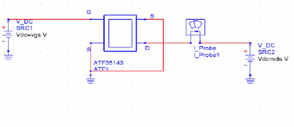
4.2 Checking the Stability
Before designing any low noise amplifier (LNA) every designer has to check the stability of the device chosen for design. Manually, the calculations are very long but it is much quicker to simulate in any circuit simulating tool, for this ADS simulator was used to check the stability of the device and it was found that the selected ATF 35143 is potentially stable to the desired frequency at 1.42 GHz. To stabilize at frequency range between 1 GHz to 1.98 GHz. one inductor value 1.8 nH was added to the source side of the first transistor. The Figure 20 and Table 3 show the stability of the device over a range from 1 GHz to 2 GHz frequencies.
Figure 20 Stability Circuit with Ideal Components Frequency (GHz) K ∆ 1.000 2.746 0.106 1.140 2.820 0.080 1.280 2.881 0.061 1.420 2.928 0.048 1.560 2.980 0.039 1.700 3.044 0.036 1.840 3.088 0.036 1.980 3.112 0.038
Table 3 K and ∆ value from 1 GHz to 2 GHz
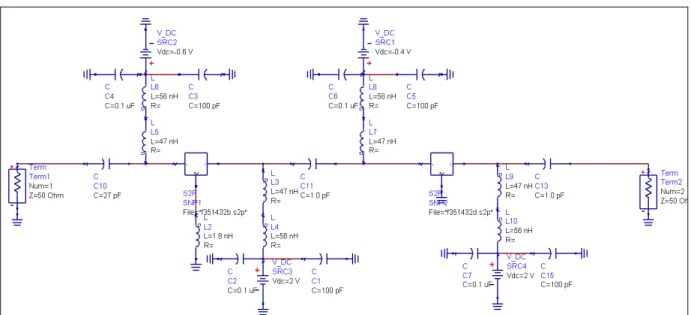
4.3 Design a Biasing and Matching Networks
The next step is to check the DC bias point of two transistors and to design corresponding biasing networks. For the desired application bias points (Vds = 2 V, Ids=10 mA) are chosen for first transistor and (Vds =2 V, Ids = 30 mA) for second transistor .The Figure 21, Figure 22, Figure 23 and Table 4 below show the dc bias set up for two transistors and the corresponding results.
LNA Design Process
Figure 22 DC Bias Curves for Two Transistors
First stage Second stage
Vds = 2 V Vds =2 V
Vgs = -0.65 V Vgs = -0.39 V
Ids =10 mA Ids =30 mA
Figure 23 Bias Networks with Ideal Components for Two Stage LNA
Next step after designing biasing networks for two transistors was to build matching circuits for two stages low noise amplifier (LNA). To design such matching networks smith chart was used from ADS software. The following Figure 24 to Figure 27 show the input, intermediate, output and total matching circuit for two stage LNA.
LNA Design Process
Figure 25 Intermediate Matching
Figure 27 Total Matching Network for Two Stage LNA
Utilizing the ideal components provided by the use of an ADS software component pallet, a two stage low noise amplifier design was proposed. Ideal components cannot be used for layout and fabrication of LNA with respect to real components. The process of amplifier layout and fabrication will be explained in layout and fabrication sections.
4.3.1 Simulation Results of Two Stage Low Noise Amplifier with Ideal Components
In this section simulated results of noise figure, scattering parameters, gain, and stability chart of proposed LNA design are showing
LNA Design Process
Figure 29 LNA Simplified Schematic Stability Plot
Figure 31 LNA Simplified Schematic Gain Plot
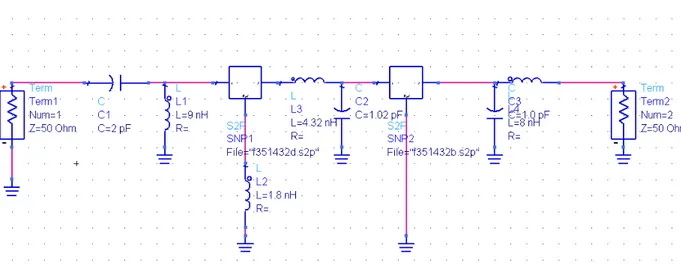
4.4 Layout of LNA
To make a layout for any RF circuits the designer needs a real component foot prints. For this task, design kit from Murata manufacturers was downloaded which includes all the real components. Finally ideal components of two stages LNA were replaced with real components and a layout using ADS software. Figure 32 to Figure 34 below shows the final layout of LNA schematic with ideal and real components and layout. The Figure 33 is divided into several parts and it is showing in the appendix section.
LNA Design Process
Figure 32 Final Schematic of LNA with Real Components
Figure 34 LNA Final Layout
Where
RFin = Input signal RFout = Output signal V1 = Gate voltage (-0.64 V)
V2 = Drain voltage (2 V)
V3 = Gate voltage (-0.40 V)
V4 = Drain voltage (2 V)
4.4.1 Simulation Results of Final Layout
The following Figure 35 to Figure 38 shows the simulated results of final layout of LNA with real components and all the graphs have taken from advanced design systems (ADS) software.
LNA Design Process
Figure 35 LNA Final Layout Schematic S-parameters
Figure 37 LNA Final Layout Schematic Noise Figure
LNA Design Process
4.5 Comparing Results
In our designed L-band two stage LNA, we used GaAs technology for the Radio Astronomy application to provide low power, low cost, operational ability over a wide range of temperature, lower noise figure and higher gain. The sub circuits in this design are similarly related to traditional LNA but still there are few slight differences. We have selected Rogers R03003 material for fabrication because of its low dielectric loss at higher frequencies and in biasing we use bipolar power sources due to their low noise figure, high gain and high efficiency. From architecture point of view, inductive degeneration architecture is used in our LNA design and finally the most important difference from other researches on LNA is that, our two stage LNA at 1.42 GHz is designed to connect, match and test together with the patch antenna used in Radio telescope systems.
In all radio telescopes, the sensitivity is the main important parameter to consider because the sensitivity of the radio telescope is used to effectively detect the weak natural radio emissions coming from the galaxies. So a noise figure is the most important parameter in radio telescope as the sensitivity is depending on its value, the smaller it is, the higher is the sensitivity of the telescope. From our simulation of two stage LNA, we achieved noise figure 0.299 dB and gain 24.25 dB. By comparing our results with LNA’s explained in references [13], [14], [15], the
difference is that RC elements have been used in the others biasing networks and matching networks, while LC elements have been used in our biasing and matching networks. Using RC networks they achieve more stability with a relatively higher noise figure but the use of LC networks gives us a lesser noise figure and less stability. Comparing our achieved results from the other previously research works on LNA (Ref [13], [14], [15]) shows that our project is much
Fabrication and Test Plan
5
Fabrication and Test plan
5.1 Fabrication of LNA
To fabricate whole two stage low noise amplifier R03003 material was used because R03003 has low dielectric loss at high frequencies. For this particular fabrication of total design R03003 material with dielectric constant εr = 3, standard thickness (T) = 0.50 mm and standard copper
cladding (U) = 17 µm was used. The data sheet of R03003 material is shown in appendix section. In order to connect the RF input signal port and output port of Fabricated LNA board to the Network Analyzer, two SMA connectors at both input and output ports were used.
Initially the fabrication work was started by selecting a material R03003 with the components case size 0603 (1.52 X 0.76) mm. But after making a layout file which is used to fabricate all the
components on the material, it was realized that it is very difficult to solder such small component case sizes. Therefore the component case sizes were changed to 1206 (3.2 X 1.6) mm in order to solder easily on the fabrication material. Now fabricated circuit is showing in Figure 39
Figure 39 Fabricated Circuit
5.2 Test Plan
The final step of this project is to test the result of the circuit board of LNA. In the process of etching board bigger die size of all the components was used for soldering purpose and for measurement. For both RF input and RF output 50 ohms transmission line was used.
Before starting the measurement of LNA, first consideration was a dc level measurement. If there is any problem in dc levels it will affect the performance of the circuit board of LNA design. In order to Test and Measure this fabricated two stage Low Noise Amplifier board, the following equipments are required.
• Power supply unit +7 V (dual power)
• Digital Multimeters
• Breadboard
• Connection wires
• Spectrum analyzer
• Network analyzer
Before going to Test the total two stages LNA, initially test was initiated by checking the bias point of an individual transistors separately on bread board.
Important precautions are to be considered before starting the measurement of LNA circuit board
• Before applying supply voltages to the transistor check all the connections carefully.
• Turn on the power supply unit
• Always start to apply the supply voltages from the gate side of the transistor slowly in steps of 0.1 V to required gate voltage.
• Slowly apply supply voltage to drain side of the transistor.
According to the DC simulations the Required Gate voltage is -0.64 V for (2 V, 10 mA) bias point in first stage and -0.39 V for (2 V, 30 mA) bias point in second stage respectively. To apply such bias voltages to the transistors precautions were to be made by providing a drain and gate resistors to the transistors. For this reason calculation of the resistor values according to two bias points of the two transistors were made, for first stage transistor the drain resistor is 200 Ω and gate resistor is 1.5 kΩ and for second stage the drain resistor is 66 Ω
Fabrication and Test Plan
Figure 41 Bias Setup for a Single Transistor in Second Stage
Then initially the bias point test was started by applying gate voltage to the Gate side of transistor and then applied the required drain voltage to the drain of the Transistor from the dual power supply unit. But whenever two supply voltages to the transistor with above arrangement were applied, no stable bias point was achieved meaning that the required bias point voltages are fluctuating. It was further tested by a spectrum analyzer, which showed that the test circuit is oscillating.
Then it was decided to change the bias set up to get a stable bias point. For this an extra feedback resistor was used (from drain to gate side of transistor) in addition to the drain resistor and gate resistor. This arrangement is show in following figures
Figure 43 Bias Setup for Second stage with Extra Feedback Resistor
Once again the test was conducted but the outcome was the same. Again test was made with spectrum analyzer to check whether the circuit is oscillating or not and it showed that the circuit is still oscillating at lower frequencies like 149 MHz and 355 MHz for two stages respectively. There are some general reasons for unstable bias point they are listed below
• Due to long connecting wires in bread board arrangement for bias point selection which will acts as like oscillator at lower frequencies.
• Any improper soldering in test board.
• Inherent design problem
Then the circuit was trouble-shoot according to above mentioned points and was tested by spectrum analyzer, which showed that again it is oscillating the required bias point. Finally it was decided to check the other reason for oscillating, which included improper soldering. After re-soldering some components, the circuit was tested again by spectrum analyzer and it shows that the circuit was still oscillating. It was decided that this problem is due to the inherent design problem and the only solution is that redesign the circuit will rectify the problem. This task was not achieved because of time restraints.
Conclusions and Future Work
6
Conclusions and Future Work
The main goal of this thesis was to design a two stage low noise amplifier for radio telescope system working at 1.42 GHz frequency to extract and amplify the received signals coming from galaxies. The thesis can be used for educational purpose in Halmstad University. Finally the designed LNA is to connect, match and test together with patch antenna to reduce the system components and signal loss.
The simulation results of the two stage low noise amplifier design and layout were successful and reached all the target specifications. In the proposal, the first stage was designed for low noise figure and second stage for high gain. From the simulation we got the noise figure 0.299 dB and gain 24.25 dB. While measuring the values from the fabricated circuit board, we found that bias point is not stable due to self oscillations in amplifier at lower frequencies like 149 MHz for first stage and 355 MHz for second stage. This problem was tackled in several ways but it did not work because of its inherent design problem.
For future work it is strongly recommended that special care is to be taken while connecting wires between components on the board and the voltage supply. Also effort to reduce the complexity of the circuit with fewer components would help. Another important point is tried to redesign the stability circuits at lower frequencies to make the circuits stable at lower frequencies. After that the designed two stage LNA can connect, match and test together with patch antenna. During this time, we feel that we have gathered and studied enormous information on how radio telescopes and low noise amplifiers (LNA) works. For simulation, advanced design systems software was used but it was new for us. We learnt a lot of new tools from this software and used them in our design process. The best thing about this work has been our experience in doing a lot of practical work
Appendix
Appendix
In this section, showing the datasheet of ATF 35143 transistor and the datasheet of material (Rogers RO3003) which is used for our fabrication process
Datasheets of ATF 35143
Table 6 Typical Noise Parameters of ATF 35143 [24]
Figure 44 MSG/MAG and | S21 |² vs Frequency
at 2 V, 10 mA [24]
Appendix
Table 7 Scattering Parameters of ATF 35143 Transistors (VDS = 2 V, IDS = 30 mA) [24]
Figure 45 MSG/MAG and | S21 |² vs. Frequency at 2 V, 30 mA [24]
Figure 46 VDS vs I DS Curve [24]
Appendix
Figure 48 Gain Charts [24]
Datasheet of Rogers’s (RO3003) Material
Here final schematic of low noise figure are divided into several parts
Figure 49 Parts 1 of Final Schematic
Appendix
Appendix
Figure 53 Parts 5 of Final Schematic
Abbreviations
Abbreviations
FET Field effect transistor
PHEMT Pseudomorphic high electron-mobility-transistor
HEMT High Electron Mobility Transistor
LNA Low Noise Amplifier
S11 Input reflection coefficient
S12 Reverse transmission gain
S22 Output reflection coefficient
S21 = Forward gain
GaAs Gallium arsenide
MESFET Metal-Semiconductor Field Effect Transistor
MMIC Monolithic Microwave Integrated Circuit
PC Personal computer
PDA Personal digital assistant ADS Advanced design systems
References
References
[1] Fraknoi, Morrison, Wolf, “Voyages Through The Universe,” 2000, Saunders college publishing, Philadelphia, ISBN: 0-03-025983-5.
[2] Raisanen, Antti, “Radio Engineering for Wireless communication and Sensor Applications,” 2003, Artech house, London, ISBN: 1-58053-669-7.
[3] Gibilisco, Sten, “Hand book of radio and wireless technology,” 1998, McGraw-Hill Professional Publishing, USA, ISBN: 0-07-023024-2
[4] Rau, A.R.P “Astronomy Inspired Atomic and Molecular Physics,” 2002, Kluwer Academic Publisher, New York, ISBN 1-40-200467-2.
[5] Xuezhen Wang, Robert Weber, “Low Voltage Low Power SiGe, BiCMOS X-band LNA Design and its Comparison Study with IEEE 802.11a LNA Design,” Conference, IEEE International, Iowa State University, Ames, 2005.
[6] Gramegna, G, “A sub-1-dB NF±2.3-kV ESD-protected 900-MHz CMOS LNA,”
IEEE Journal of Solid State Circuits, Vol. 36. P.1010 – 1017, July 2001.
[7] Gatta, F, “A 2-dB noise figure 900-MHz differential CMOS LNA,” IEEE Journal of Solid-State Circuits, Vol. 36. P.1444 – 1452, Oct. 2001.
[8] Hung-Wei Chiu, “A 2.17-dB NF 5-GHz-band monolithic CMOS LNA with 10-mW DC power consumption,” IEEE Transactions on Microwave Theory and Techniques, Vol. 53, P.813 – 824, March 2005.
[9] Guochi Huang, “Post linearization of CMOS LNA using double cascade FETs”, Circuits and Systems, 2006. ISCAS 2006. Proceedings 2006 IEEE International Symposium on 21-24, May 2006.
[10] Namsoo Kim, “A cellular-band CDMA 0.25/spl mu/m CMOS LNA linearized using active post-distortion,” IEEE Journal of Solid-State Circuits, Vol. 41, No. 7,
July. 2006.
[11] Adiseno, “A 1.8-V wide-band CMOS LNA for multiband multistandard front-end receiver,” Solid-State Circuits Conference, 2003. ESSCIRC '03, P.141 - 144, Sept. 2003.
[12] Wei Guo “Noise and linearity analysis for a 1.9 GHz CMOS LNA,” Circuits and Systems, 2002. APCCAS 2002 Asia Pacific conference on Vol. 2, P.409 – 414, Oct. 2002.
[13] R. Benton et al., “GaAs MMICs for an integrated GPS front-end,” GaAs-IC Symp, Technical Digest 1992, 14th annual IEEE 4-7 Oct. 1992 page(s) 123–126.
[14] K. R. Cioffi, “Monolithic L-band amplifiers operating at milliwatt and sub-milliwatt DC power consumptions,” IEEE Microwave and Millimeter-Wave Monolithic Circuits Symp. Dig., June 1991, pp.9-12.
[15] Y. Imai, M. Tokumitsu, and A. Minakawa, “Design and performance of low-current GaAs MMIC’s for L-band front-end applications,” IEEE Trans. Microwave Theory Tech., vol. 39, pp. 209–215, Feb. 1991.
[16] Derek K. Shaeffer, “1.5-V, 1.5-GHz CMOS Low Noise Amplifier,” IEEE Journal of solid-state circuits, Vol. 32, No. 5, May 1997.
Academic Publisher, New York, ISBN: 0-7923-7551-3, 2001
[18] Rohde, Ulrich L, “Communication Receivers: Dps, Software Radios and Design”, 2000, McGraw-Hill Professional Publishing, USA, ISBN: 0-07-136121-9.
[19] Guillermo Gonzalez, “Microwave Transistor Amplifiers Analysis and Design,” 1997, Prentice Hall, N.J., ISBN: 0-13-254335-4.
[20] Karris, Steven T, “Electronic Devices and Amplifier Circuits with MATLAB Applications,” 2005, Orchard Publications, USA, ISBN: 0-9744239-4-7.
[21] Chris Bo wick, “RF Circuit Design,” 1982, Library of congress cataloging in publication data, UK, ISBN: 0-7506-9946-9.
[22] LNA Design Using Spectre RF Application Note, Product version 5 (2003-2004). [Online]Available:
http://www.ek.isy.liu.se/~jdab/SpectreRF_LNA533AN.pdf
[23] R.H:Witvers, J.G.Bij de Vaate, “MMIC GaAs and InP Very Low Noise Amplifier Designs for the Next Generation Radio Telescope”, Netherland.
[24] Avago Technologies Stuff, “ATF-35143 Low Noise Pseudomorphic HEMT in a Surface Mount Plastic Package,” Avago Technologies, USA, Tech. 5989-3748EN
January 9, 2006.
[25] Advanced Circuit Materials Stuff, “RO3000 Series High Frequency Circuit Materials,” Rogers’s Corporation, USA, Publication #92-130.
References
Permission
Figure 44 - 48 and Table 5 - 8 “The ATF 35143 data sheet is the copyrighted material of Avago Technologies and is used with their permission”
![Figure 7 Two Port Networks [19]](https://thumb-eu.123doks.com/thumbv2/5dokorg/5461345.141854/26.892.107.759.197.1125/figure-two-port-networks.webp)
![Figure 8 Fixed Bias [20]](https://thumb-eu.123doks.com/thumbv2/5dokorg/5461345.141854/29.892.206.698.359.666/figure-fixed-bias.webp)
![Figure 9 Collector to Base Bias [20]](https://thumb-eu.123doks.com/thumbv2/5dokorg/5461345.141854/30.892.207.698.515.825/figure-collector-to-base-bias.webp)
![Figure 14 Constant Reactance Circles [21]](https://thumb-eu.123doks.com/thumbv2/5dokorg/5461345.141854/34.892.261.585.310.693/figure-constant-reactance-circles.webp)
![Figure 15 Combination of Z and Y Smith Chart [21]](https://thumb-eu.123doks.com/thumbv2/5dokorg/5461345.141854/35.892.108.595.392.865/figure-combination-z-y-smith-chart.webp)
![Figure 18 Showing the Basic Diagram of Matching Network for One Device [21]](https://thumb-eu.123doks.com/thumbv2/5dokorg/5461345.141854/38.892.117.727.205.511/figure-showing-basic-diagram-matching-network-device.webp)