Linköping University Post Print
Photoluminescence study of
nanocrystalline-Si(Ge) embedded in mesoporous silica
Bouchaib Adnane, Yi-Fan Lai, Jia-Min Shieh, Per-Olof Holtz and Wei-Xin Ni
N.B.: When citing this work, cite the original article.
Original Publication:
Bouchaib Adnane, Yi-Fan Lai, Jia-Min Shieh, Per-Olof Holtz and Wei-Xin Ni, Photoluminescence study of nanocrystalline-Si(Ge) embedded in mesoporous silica, 2009, SOLID-STATE ELECTRONICS, (53), 8, 862-864.
http://dx.doi.org/10.1016/j.sse.2009.04.014
Copyright: Elsevier Science B.V., Amsterdam.
http://www.elsevier.com/
Postprint available at: Linköping University Electronic Press
Photoluminescence Study of Nanocrystalline-Si(Ge) Embedded in
Mesoporous Silica
Bouchaib Adnane1*, Yi-Fan Lai2, Jia-Min Shieh2, Per-Olof Holtz1, and Wei-Xin Ni1, 2
1
Dept. of Physics, Chemistry and Biology, Linköping University, S-581 83 Linköping, Sweden
2
National Nano Device Laboratories,
26 Prosperity Road I, Hsinchu, Taiwan 30078, R.O.C
Abstract
Photoluminescence (PL) properties of mesoporous silica (MS) samples incorporated with Si or Ge nanocrystals (nc) have been investigated with various excitation powers and post RTA processes. The analysis of experimental results revealed a superlinear intensity dependence (m = 1.7) in the MS reference sample without nanocrystals, while a sublinear behavior (m = 0.8) is observed for the nc-Si in MS. It thus suggests the same recombination responsible for the luminescence at ~2.75 eV for both samples, but different kinetic limitations for the carrier transfer processes. Si nanocrystals play in this case an important role in generating more photoexcited carriers, enhancing the PL intensity.
Keywords: Mesoporous silica; Nanocrystals, Photoluminescence, Power dependence, Thermal annealing.
*
Corresponding author. Address: Department of Physics, Chemistry & Biology (IFM), Linköping University, S- 581 83 Linköping, Sweden.
Tel.: +46 13 281182; fax: +46 13 137568. E-mail address: bouad@ifm.liu.se.
1. Introduction
Due to observation of luminescence at room-temperature (RT) over a wide spectral range from blue to red [1] and also the possible gain mechanisms [2,3], self-assembled Si or Ge nanocrystals (nc) in silica-based materials have attracted a lot of interests during recent years for potential applications in photonics and other nano-structured devices [2]. Si(or Ge) nanocrystals in a silica material can be prepared using different techniques. The most frequently used technique is the precipitating process through thermal annealing of the Si-rich SiO2 layer obtained by either ion implantation or plasma enhanced chemical vapour deposition (PECVD). The latter is an easier process to perform but somewhat more difficult in controlling the size and density of synthesized semiconductor nanocrystals. Furthermore, it is known that the optical properties of such nanostructured Si(Ge)/SiO2 materials varied depending on the details of the synthesis technique and the materials system [3-6].
Mesoporous silica (MS) with extremely large internal surface area has served as a useful template material to accommodate high density and uniform Si(Ge) nanocrystals, owning to its adjustable and uniform pore sizes in the range of 1.5 to 10.0 nm. Such a material system is called nanocrystalline-Si embedded in mesoporous silica (nc-Si in MS). Its open and highly interconnected sponge-like porous structure can also be used to fill with other photosensitive materials, or conveniently used as a host or template for polymers, catalysts, or nanoparticles.
Recently, Shieh et al successfully prepared MS templates using the Sol-Gel technique, and subsequently embedded the template with nc-Si(Ge) using various atomic deposition processes [7] for observation of the enhanced photoluminescence (PL) at RT. Some interesting applications based on devices involving nc-Si(Ge) in MS in the active region [8] were subsequently explored. However, there is still limited characterization and a lack of detailed understanding of the optical properties, in
particular the light emission mechanisms and their dependence on the sample preparation process of these Si-based photonic materials
In this communication, we present the results of a PL study on MS samples embedded with nc-Si(Ge). The PL measurements were mainly performed at low temperature, in order to reduce any thermally activated processes, while the experiments with various excitation powers and annealing processes were carried out with an aim to investigate the origin of the light emission and for providing more understanding and insight of the optical properties.
2. Experimental
The MS templates were prepared by spin-coating on p-type Si substrates with a 5-nm-thick SiO2 buffer layer on top using the Sol-Gel technique, which could produce MS films with a pore-size of 4-5 nm and a pore-wall of ~1.5 nm [7]. The thickness of all used MS films was ~220 nm. Si or Ge nanocrystals were then synthesized in the MS templates using a pulse-modulated high-density inductively coupled plasma (ICP) deposition process [9], but in the present study most of the samples were only embedded with nc-Si. During the deposition, a negative voltage of 40 V at 300 kHz was applied on the substrate. This creates preferential growth of nc-Si on the bottom of the pore-channels. Depending on the detailed deposition conditions and the number of cycles used for the whole process, the nano-pores in MS could be fully or partially filled by Si nanocrystals. For the samples used in this work, only two deposition cycles were used and accordingly, the MS are partially filled with Si nanocrystals. Finally, a 10-nm-thick SiO2 layer was deposited on the MS film.
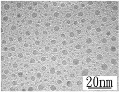
The average size of the nc-Si was about 4 nm in diameter, as revealed by a cross-sectional image of the transmission electron microscopy (XTEM) in Fig. 1. The areal density of nanocrystals was estimated to be at a level of ~5x1014 cm-2, which is among
the highest compared to what is achieved by other synthesis techniques [3]. Due to the foil thickness, however, it is difficult to draw conclusions on the filling effect of Si in the pores.
Fig. 1. Cross-sectional TEM image of a mesoporous silica film embedded with high density nc-Si.
The PL experiments were performed mainly at 2 K in a He-flow cryostat using an optically pumped deep UV Monolithic Block Doubler (MBD) laser ( =266 nm) as the excitation source with the optical power density varied from 0.1 to 10 Wcm-2. The laser beam was focused by a (10 cm) UV lens into a 1 mm2 spot diameter. The samples were oriented to the laser beam by 45º. The emitted luminescence was collected in a conventional 90º geometry and dispersed by a one meter SPEX 1404 double-grating monochromator with two 1200 lines/mm gratings. The spectra were finally recorded by a Gallium Arsenide (GaAs) photomultiplier detector (peak wavelength 300-800 nm) using a standard lock-in technique and gated electronics (SR-510, Stanford Research Systems). A set of optical filters were used in order to cut stray radiation from the laser beam and scattered light from the samples.
3. Results and discussion
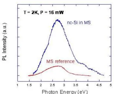
The PL spectra of nc-Si embedded in MS, together with a reference MS template with no incorporation of any nc-Si are presented in Fig. 2. The spectral shapes are rather similar for the two samples with a broad-band emission peaking at ~2.75 eV. The luminescence is however much more intense for those embedded with Si or Ge nanocrystals which exhibits a similar spectrum (not shown here). This implies that the emission mechanism for MS samples with or without nc-Si(Ge) could be the same, but the incorporation of nc-Si(Ge) enhances considerably the luminescence intensity. According to the literature [10-13], the PL at ~2.75 eV is characteristic for both bulk amorphous and crystalline SiO2, in which the laser heated electron-hole plasma could be condensed on self-trapping exciton states, e.g. neutral defects of oxygen vacancy (≡Si-Si≡) [14,15] on surface, for emission. Since the present MS samples are
only partially incorporated with filled nc-Si, it is reasonable to assume that the light emission was still governed by the surface properties of silica. The semiconductor nanocrystals hence play a role by sensitizing the luminescence emission through generating more photo-excited carriers. These carriers are then trapped in the defect state e.g. the interfacial oxygen defect sites and subsequently recombine to increase the PL intensity.
Some samples were post-treated by rapid thermal annealing (RTA) at 950 °C for 15 - 75 seconds in an N2 ambient. PL spectra of nc-Si samples before and after RTA are depicted in Fig. 3. Although there was no evident energy shift of the PL peak, the RTA process in this study quenched the luminescence severely. There was an inverted relation between the RTA processing time and the PL intensity, as shown by the data points summarized in the insert of Fig. 3. This behavior is different from reported results in the literature, for which nc-Si samples prepared by other techniques, the post RTA process usually resulted in an enhancement of the PL intensity, probably due to the removal of point defects. Therefore, we again attribute the PL quenching effect to the nature of partially filled nc-Si structures. The thermal annealing would in this case alter the morphology and interface properties of nanocrystals, which thus affect the carrier transfer efficiency and eventually the PL intensity. For the extreme case, after annealing in a conventional furnace at 1000 ºC for 2 hours, the PL at 2.75 eV completely vanished. Instead a weaker but narrower PL peak at ~1.77 eV was observed [8], which was regarded as the evidence that the originally partially filled nc-Si became the fully isolated nc-Si after a long annealing. The observed PL was then due to the band-to-band recombination of carriers and the PL energy position corresponds well to the quantum-confinement effect in relation to the size of nanocrystals [13].
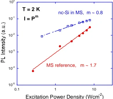
Although the shape of the PL spectra with and without incorporation of Si nanocrystals was similar, the excitation power dependence of the PL intensity revealed a significant difference, as shown in Fig. 4 in double logarithmic scale. The dependence of the steady-state PL intensity (I) on the excitation power (P) is usually approximated by a power law function, i.e. I = Pm. For the MS reference sample, a superlinear behavior was observed with the coefficient m = 1.7, i.e. close to quadratic. However, for the MS samples embedded with nc-Si the dependence became sublinear (m = 0.8). Note
that the superlinear behavior occurred in the MS sample when the PL intensity was rather low. In this case, the PL emission could be governed by the generation of non-equilibrium carriers that were first captured by the acceptor- or donor-like states, respectively, on the SiO2 surface for the radiative recombination.
Fig. 3. PL spectra of nc-Si in MS with or without the 950 ºC RTA process. The integrated PL intensity vs. the RTA time is plotted in the insert.
10-5 10-4 10-3 10-2 10-1 100 0.1 1 10 T = 2 K I = Pm
Excitation Power Density (Wcm-2) nc-Si in MS, m ~ 0.8
MS reference, m ~ 1.7
Fig. 4. Excitation power dependence of the integrated PL intensity for nc-Si in MS and reference samples.
With embedding of partially filled nc-Si in the MS, there still remains a large surface area of silica, such that PL would be dominated by the same recombination namely between localized electrons and holes at the nc-Si/SiO2 interface. But in this case the enhanced luminescence intensity is expected, because more carriers could be generated by photo-excitation of semiconductor nanocrystals. However, firstly the density of the interface states is limited and secondly the carrier transfer from the Si nanocrystals to the interface emission sites could also be a kinetically limited process, the PL intensity could quickly saturate. It thus explains why the m-coefficient decreased to 0.8.
4. Conclusions
PL of MS samples without and with nc-Si(Ge) incorporation have been studied. The results of the RTA and excitation power dependence experiments suggest the significance of interface defect sites and the same mechanism for both samples for the luminescence at ~2.75 eV, i.e. due to the radiative recombination of localized electrons and holes at the interface. We particularly point out to the role of nanocrystals in generating more photoexcited carriers, thus enhancing the PL intensity.
These experimental findings combined with further characterizations of these MS materials with nc-Si(Ge) notably at different temperatures can help us to understand the origin and nature of light emission in nc-Si in materials.
References:
[1] J.-Y. Zhang. X.-M. Bao, Y.-H. Ye, and X.-L. Tan, Appl. Phys. Lett. 73, 1790 (1998).
[3] L. Pavesi, L. Dal Negro, C. Mazzoleni, G. Franzo, and F. Priolo, Nature 408, 440 (2000).
[4] P. Mutti, G. Ghislotti, S. Bertoni, L. Bonoldi, G. F. Cerofolini, L. Meda, E. Grilli, and M. Guzzi, Appl. Phys. Lett. 66, 851 (1995).
[5] L. S. Liao, X. M. Bao, X. Q. Zheng, N. S. Li, and N. B. Min, Appl. Phys. Lett. 68, 850 (1996).
[6] K. S. Zhuraviev, A. M. Gillinsky, and A, Yu Kobitsky, Appl. Phys. Lett. 73, 1046 (1998)
[7] J. M. Shieh, A. T. Cho, Y. F. Lai, B. T. Dai, F. M. Pan, and K. J. Chao, Electrochem. Solid-State Lett. 7, G319 (2004).
[8] J.-M. Shieh, Y.-F. Lai, and W.-X. Ni, Appl. Phys. Lett. 90, Art. No. 051105 (2007). [9] A.-T. Cho, J.-M. Shieh, J. Shieh, Y.-F. Lai, B.-T. Dai, F.-M. Pan, H.-C. Kuo, Y.-C.
Lin, K.-J. Chao, P.-H. Liu, Electrochem. Solid-State Lett. 8, G143 (2005).
[10] N. Chiodini, F. Meinardi, F. Morazzoni, A. Paleari, R. Scotti, D. Di Martino, Appl. Phys. Lett. 76, 3209 (2000).
[11] B. Yao, H. Shi, X. Zhang, L. Zhang, Appl. Phys. Lett. 78, 174 (2001).
[12] Y. D. Glinka, A. S. Zyubin, A. M. Mebel, S. H. Lin, L. P. Hwang, and Y. T. Chen, Eur. Phys. J. D16, 279 (2001).
[13] A. Anedda, C.M. Carbonaro, F. Clemenete, R. Corpino, and P. C. Ricci, Materials Science & Engineering C25, 631 (2005).
[14] Y. D. Glinka, S. H. Lin, and Y. T. Chen, Phys Rev. B66, Art. No. 035404 (2002). [15] M. V. Wolkin, J. Jorne, P. M. Fauchet, G. Allan, and C. Delerue, Phys. Rev. Lett. 82,