Master of Science Thesis
M D S A B B I R A H S A N
Experimental Setup of High Harmonic
Generation Based Angle Resolved
Photoemission Spectroscopy
(HHG-ARPES) and Test Measurement on
Tungsten (W) [110] Surface
K T H I n f o r m a t i o n a n d C o m m u n i c a t i o n T e c h n o l o g y
Experimental Setup of High Harmonic
Generation Based Angle Resolved
Photoemission Spectroscopy
(HHG-ARPES) And Test Measurement
on Tungsten (W) [110] Surface
M D S A B B I R A H S A N
Master of Science Thesis
Stockholm, Sweden 2013
A Thesis submitted for the degree of Master of Science
Experimental Setup of High Harmonic
Generation Based Angle Resolved Photoemission
Spectroscopy and test measurement on Tungsten
W(110) surface
Md Sabbir Ahsan December 20, 2013
Performed
Ultrafast X-ray Physics group Faculty of Physics
Ludwig Maximilians University(LMU) Munich,Germany
Supervisor Prof.Dr.Ulf Kleineberg
LMU,Germany Examiner
Docent. Jonas Weissenrieder KTH,Sweden
School of Information and communication Technology Royal Institute of Technology (KTH)
Contents
Acknowledgement vii
abstract viii
1. Introduction 1
1.1. Significance of studying the surface state: . . . 2
1.2. Goal of the Thesis . . . 2
1.2.1. Familiar with Ulrashort pulse Generation and application to gen-erate attosecond pulse: . . . 3
1.2.2. Experimental setup . . . 3
1.2.3. Experimental Study . . . 3
1.3. Thesis structure: . . . 4
I. Theoretical Background: 5 2. Bandstructure and Fermi surface of solid 6 2.1. Free electrons in solid: . . . 6
2.2. Energy Bands in a solid: . . . 8
2.2.1. Electron in a weak periodic potential: . . . 9
3. Spectroscopic Methods to study surface state 15 3.1. Photoelectron Spectroscopy: . . . 15
3.1.1. Kinematic of photoemission . . . 16
3.1.2. Linear response in external field: . . . 18
3.1.3. Dipole approximation and selection rule: . . . 19
3.1.4. Model for Photoemission process . . . 21
3.1.5. Surface and bulk sensitive photoemission . . . 23
3.2. ARPES tools: . . . 24
3.2.1. Hemispherical electron analyzer: . . . 24
3.2.2. Time of flight analyser (TOF) . . . 24
3.3. Auger Spectroscopy: . . . 25
3.3.1. Principle: . . . 25
4. Generation of Ultra-short pulses: From femtosecond laser to attosecond XUV pulse 27 4.1. Mathematical Idea of an ultra-short pulse: . . . 27
Contents
4.2. Basic element for generating ultrashort pulse . . . 29
4.2.1. Gain Medium . . . 29
4.2.2. Mode locking technique . . . 29
4.2.3. Dispersion control and pulse compression . . . 30
4.2.4. Principle of Dispersion compensation . . . 32
4.2.5. Mirror and output Coupler . . . 34
4.3. Ionization process in strong laser field . . . 34
4.4. Generation of attosecond pulse: High Harmonic Generation . . . 36
4.5. Measuring the pulse duration: . . . 38
4.5.1. Autocorrelation Technique . . . 38
4.5.2. Stereo ATI: . . . 39
4.5.3. Attosecond streaking experiment . . . 40
II. Experimental setup,results and discussion 42 5. Experimental setup of HHG Based ARPES 43 5.1. Generation of attosecond XUV pulse . . . 43
5.1.1. Generation of few cycle pulse . . . 43
5.1.2. HHG setup . . . 46
5.2. Sample preparation chamber . . . 47
5.2.1. evaporation chamber . . . 47
5.2.2. cleaning chamber . . . 48
5.2.3. Conditioning filament . . . 49
5.3. ARPES Chamber . . . 49
5.3.1. sample heater and sputter gun . . . 50
5.3.2. Double Mirrors . . . 50
5.3.3. Magnetic field compensation . . . 51
5.3.4. Ultra high vacuum in ARPES . . . 53
5.3.5. Connection: Beamline, ARPES and Sample preparation . . . 56
5.4. Characterization of experimental setup . . . 56
5.4.1. Determining laser spot size after HCF . . . 56
5.4.2. Finding the focus point . . . 57
5.4.3. Energy and time resolution . . . 58
5.4.4. Determining the time offset . . . 59
6. Experimental study on Tungsten W(110) surface 60 6.1. Auger spectroscopy on Tungsten(110) . . . 60
6.1.1. Detection of surface contamination . . . 60
6.1.2. Sample cleaning: Method and verification . . . 62
6.2. Crystal property of Tungsten(W) . . . 64
6.3. Photoemission Spectroscopy on Tungsten (W) . . . 65
6.3.1. Observation of Conduction band Spectrum . . . 66
Contents
6.3.3. Bandstructure observation . . . 70
III. Future work: Improvement, conclusion 72
7. future work 73
7.1. Area of improvements: . . . 73 7.2. Prospect for time resolved (TR) study:(TR-ARPES) . . . 75
8. Conclusion 77
A. Calibration of evaporation chamber: 78 B. Helmholtz compensation 79
List of Figures
2.1. Electron in an uniform potential . . . 6
2.2. Fermi surface in free electron model . . . 7
2.3. Formation of energy bands in a solid . . . 9
2.4. Bandstructure representation of a solid . . . 11
2.5. Magnitude of energy gap at zone boundary . . . 13
2.6. Variation in potential energy . . . 13
2.7. Band gap of a solid . . . 14
2.8. Effect of weak periodic potential on Fermi surface . . . 14
3.1. Photoelectron spectrum . . . 16
3.2. Photoemission Geometry . . . 17
3.3. Photoemission process . . . 18
3.4. Photoemission model . . . 22
3.5. Energy dependent mean free path . . . 23
3.6. ARPES electron analyzers . . . 25
3.7. Auger process . . . 26
4.1. Diagram of an ultrashort pulse . . . 27
4.2. Mode locking mechanism . . . 29
4.3. Kerr-lens mode-locking . . . 31
4.4. self-phase modulation . . . 33
4.5. Ionization field in strong Laser field . . . 34
4.6. Regimes of Nonlinear optics . . . 35
4.7. higher order harmonic generation process. . . 37
4.8. HHG Spectrum . . . 37
4.9. Autocorrelation technique to measure pulse duration . . . 38
4.10. Measuring few fs pulse duration . . . 40
4.11. Attosecond streaking experiment . . . 41
5.1. Chirped pulse amplification to generate femtosecond pulse . . . 44
5.2. Generation of ultrashort pulse . . . 45
5.3. Generation of few cycle laser pulse . . . 45
5.4. Higher order harmonic spectrum . . . 46
5.5. Sample preparation setup . . . 48
5.6. tr-ARPES experimental setup . . . 49
List of Figures
5.8. Reflectivity of double mirror . . . 51
5.9. Effect of magnetic field in PES . . . 52
5.10. Helmholtz like compensated ARPES chamber . . . 52
5.11. Ultra High Vacuum system . . . 55
5.12. 3D view of HHG based ARPES experimental setup . . . 56
5.13. Determing spot size after HCF . . . 57
5.14. Harmonic recorded in CCD camera . . . 58
5.15. Determing Energy and time resolution . . . 58
5.16. Determing time offset . . . 59
6.1. Diagram for Auger and Photoemission process . . . 60
6.2. focusing electron beam on the sample surface . . . 61
6.3. Auger Process in Tungsten surface . . . 61
6.4. Auger Spectroscopy to verify surface cleanliness . . . 63
6.5. Auger peaks from clean W surface . . . 64
6.6. direction and detector position . . . 65
6.7. Exciting sample surface with XUV photons . . . 65
6.8. photoelectron Energy spectrum . . . 66
6.9. W Photoelectron cross section . . . 67
6.10. photoelectron energy spectrum . . . 68
6.11. Fermi Surface of Tungsten(110) . . . 69
6.12. Fraction of Brillouin zone using current experimental setup . . . 69
6.13. Tungsten Bandstructure . . . 70
6.14. Theoretical Bandstructure of Tungsten . . . 71
7.1. Separation of harmonics through grating . . . 73
7.2. Time-resolved ARPES study . . . 76
A.1. Calibration of dual electron beam evaporator . . . 78
List of Tables
5.1. Magnetic Field compensation . . . 53 5.2. mean free path . . . 54
Acknowledgement
First of all, I am extremely grateful to my GOD ALLAH for giving me the mental, physical strength as well as my enthusiasm to acquire knowledge far from my country in Sweden and Germany.
I would like give special thanks and express my gratefulness to Prof. Dr.Ulf Kleineberg acting as my supervisor at Ludwig Maximilians University (LMU), Munich and Docent. Jonas Weissenrieder as my Examiner in Royal Institute of technology (KTH), Sweden. Prof. Kleineberg give me the opportunity to do my master thesis in his Ultrafast X-ray Physics Research group as an exchange student at LMU, Munich that enables me to be familiar with state-of-the-art attosecond science and technology. Based on my career goal and personal interest doing my master thesis in his research lab was the best decision for me. Also, I am very happy to get Dr. Jonas as my examiner. His nice supervision from KTH through Phone conversation and frequent emails also helped me to find my goals and direction during my thesis work in abroad. Now, I understand very nicely, I would not get better supervisor, examiner, colleagues, office mates and better environment to carry on my master thesis.
I am also grateful to Juergen Schmidt to whom I worked most of the time during my thesis work. To be honest, I never had experience to work with such complex instru-mental setup. Initially, Juergen helped me a lot to be familiar with every Instrument and how to operate. Although, it took several times for him to describe me the same things, but he always seems to be enthusiastic to explain me every setup. Moreover, I got better understanding to handle such high power laser from him. Juergen helped me a lot to finish my thesis work at the right time. His hard working effort make it possible to generate HHG based XUV attosecond pulse after severe laser breakdown for several months. I greatly admire his friendly attitude towards me during my thesis work.
My Special thanks also goes to Soo Hoon Chew to whom I contacted first and express my interest to work in their Ultrafast X-ray research lab. She helped me a lot to come in Munich for doing my thesis work. I learned many things from her advice. I also wanted to express my thanks to Alexander Guggenmos, for giving me access and to use DEKTEK tool in his well equipped clean room lab at MPQ (Max-Plank Institute of Quantum Optics). Finally, I want to give thanks every group members Kellie, Christian, Jeryl, Huaihai, Clemens,Sebastian in our research group.
abstract
Experimental set up of High harmonic Generation based angle resolved photoemission spectroscopy (HHG based ARPES) has been developed and characterized. The setup is intended for ultrafast time resolved measurement of bandstructure dynamics on the attosecond time scale. As a first proof of principle experiment HHG based ARPES measurement on a tungsten W (110) sample was done in a static mode.
Initially 27 femtosecond (fs) laser pulse was generated by chirped pulse amplification (CPA) technique from a femtosecond laser source and a hollow core fiber was used to produce few cycle (∼ 4f s) laser pulse. This Few cycle pulse ionize neon atoms and generates ultrafast attosecond (as) extreme ultra violet (XUV) pulses via HHG pro-cess that propagates towards the ARPES chamber in a ultrahigh vacuum condition (< 10−8mbar). Helmholtz like magnetic field compensated HHG based ARPES cham-ber was designed in combination with a multilayer broadband (5 eV) XUV mirror at photon energy 65 eV with a 10 kHz repetition rate. A time-of-flight (TOF) electron analyzer was installed in the UHV ARPES chamber that can collect and analyze the photoemitted electrons within an acceptance angle of ±13 degrees. Besides the HHG based ARPES chamber, a sample preparation chamber was developed and calibrated that can be used either to grow thin-film or clean the sample. Performing photoemission using highly surface sensitive 65 eV XUV photon source demands an extremely clean sample surface. As a result sample surface cleaning was performed by high temperature heating in a cleaning section of the preparation chamber before photo-exciting with the XUV pulse. Auger spectroscopy was employed by a 50 kHz pulsed electron source to verify the surface cleanliness. Finally, the attosecond XUV pulse has been focused onto the tungsten sample using the multilayer XUV mirror to investigate the conduction band photoemission spectra, Fermi edge and Fermi surface as well as energy bands of the W sample surface. Pronounced conduction band features in the photoelectron energy dis-tribution spectra were observed. The W energy bands are characterized by high density of states near the Fermi level where Fermi surface is characterized by symmetrical lobes in vertical and horizontal direction. Moreover, the available setup will be prepared for time-resolved (pump-probe) experiments using an appropriate double mirror delay unit. Following the excitation of the sample surface with a few cycle laser (pump) pulse, the time resolved electron dynamics can be monitored using XUV attosecond (probe) pulses in attosecond timescale.
Keywords: Attosecond XUV pulse, Magnetic compensation, E-beam evaporation, An-gle resolved Photoemission Spectroscopy, Auger Spectroscopy, Tungsten(110).
Chapter 1.
Introduction
Our science and technology is getting smarter day by day. Such smartness is marked by considering how fast the devices can work and how small they may be build. Our computers are getting smaller and faster but we are not satisfied. Our demand is quan-tum computer. With the remarkable advancement in the field of nanotechnology we are about at the limit in spatial dimension but still many things to be understood in shorter timescale limit. In that respect, ultrashort light sources can be used to study the nanostructure or few nanometer surface layer for better understanding about those sys-tem that can respond to the lower time scale i.e near attosecond region. High Harmonic Generation (HHG) based Angle resolved photoemission Spectroscopy (ARPES) can be such a tool where one can study the physics on the attosecond scale.
ARPES has already been proven to be a standard Spectroscopic technique to study solid state system. In a solid systems, ARPES can provide many information about the surface state, electronic bands, density of states etc. The observation of the electron dynamics in a solid state system requires proper integration of a pulsed light sources with ARPES. The shorter the pulse the shorter the event that can be observed.
With the development of ultrashort few cycle pulses and novel attosecond light sources through HHG process, an approach was taken to combine the novel light sources with the state-of-the-art ARPES tool. At present, ARPES is well established using either any Synchroton or HHG sources driven by solid state laser sources that deliver pulses in picosecond (10−12s) or > 100 fs (10−15 s) range. but the tool is not developed using a light source that deliver pulses of few fs or as(10−18 s) range. When the pulse gets shorter, the spectral shape of the pulse gets broader and vice versa1. That means a physical phenomena can be sampled on a timescale with better time resolution than any other sources. But On the other hand, one has to compromise with poor energy resolution.
Following the development of HHG based ARPES, first test measurement was per-formed in static mode to study the Tungsten (W) surface. Having novel light sources in hand, one can study the static as well as the dynamic process on the surface state.
1
Space charge effect can dominate during photoemission when using high repetition rate laser pulse but the current setup has no such effect due to low repetition rate of 10 kHz.
Chapter 1. Introduction
1.1. Significance of studying the surface state:
Surface state has drawn lot of interest to the scientific community since last decade [1–4]. There are many interesting phenomena going on in the surface state i.e solid-vacuum, solid-liquid, solid-gas etc. One can explore light matter interaction, quasi particle in-teraction, motion of electrons in the surface electronic bands [5]. The fundamental properties of a solid is encoded in the energy bands or bandstructure. As a result new state of matter can be discovered by studying the surface states or surface bands as well as the bulk bands. Recently discovered Topological Insulators [6] (TI) is the result of such study. TI surface states can offer persistent current flow [7] that can be used for quantum computation.
New device application can also be found by examining a modified surface layer by growing a thin layer on top of the substrate. Such work has been published [8] to understand about ultrafast magnetisation. An anti-ferromagnetic few nanometer thick layer has been grown between two ferromagnetic layers. Exciting the top layer with a ultashort laser pulse the magnetization has been transferred to the third layer within a timescale of few femtosecond.
Moreover, to understand the current flow one needs to understand the change of occupancy of the states near the topmost filled energy level called ”Fermi surface” and the shape of the Fermi surface determines the response due to electric, magnetic or thermal gradient. One can also find the superconductivity and magnetism simultaneously at the interface of two band insulator [9]. In general, studying surface phenomena has great impact on understanding the behavior of fundamental properties i.e. magnetization, superconductivity, electronic motion and correleation in complex system etc.
W (110) was chosen for surface study for two reasons. It is relatively easy to prepare and has high density of states near the Fermi edge which is perfect for the first time doing experiments on the newly build HHG based ARPES setup. Fermi level in W lies on the conduction band. Following the excitation on W surface using HHG beamline one can examine bandstructure, conduction band photoelectron spectrum as well as Fermi surface to understand the fundamental properties of W.
1.2. Goal of the Thesis
My initial plan was to study the ultrafast electron dynamics in solid surface, but due to instrumental breakdown as well as time constraint it has not been possible at this point. The aim of the thesis work was to get access into the emergent state-of-the-art Attosecond science and technology and apply such technological advancement in ARPES experiment. The goals can be divided into few steps.
Chapter 1. Introduction
1.2.1. Familiar with Ulrashort pulse Generation and application to generate attosecond pulse:
The Preliminary stage of my thesis work was to familiar with the theoretical concept of attosecond science and technology through literature study. Moreover, I develop some intuitive knowledge to study ultrafast phenomena such as studying cooper-pairs, band-structure dynamics etc. As a result, Special effort and concentration was to be familiar with the generation of ultrashort broad bandwidth few cycle laser pulses, experimental optics, HHG process and apply such coherent pulses to study physical phenomena. Dur-ing thesis work a summer school visit to DESY(Deutsches Electron Synchroton) also enrich my knowledge to become familiar with other coherent light sources such as Synchroton radiation and FEL (Free Electron Laser).
1.2.2. Experimental setup
HHG-ARPES chamber: Attosecond extreme ultra-violet (XUV) pulses were gener-ated from HHG process by ionizing Ne atoms from a few cycle Infrared (IR) laser pulse and both of the pulses propagate collinearly to the experimental chamber. The connec-tion between beam line and ARPES chamber has been established. Two ultra thin metal filters have been used to separate the XUV beam from IR beam for our experiment.
A complete setup of HHG based ARPES chamber has been developed that includes double mirror2, magnetic field compensation system, sample heater3, installing electron gun and sputter gun, maintaining ultra-high vacuum (UHV) condition etc. A time-of-flight (TOF) spectrometer has been installed to analyze the electrons from the sample surface (E(kx, ky)). After development subsequent calibration of the TOF spectrome-ter was done to find energy and time resolution, time zero offset for both Auger and photoemission spectroscopy.
Sample preparation chamber: A sample preparation chamber was developed during thesis work that contains sample cleaning chamber and electron beam evaporation for thin film fabrication. This chamber has been attached with the ARPES chamber. The evaporation chamber was also calibrated using four different materials.
1.2.3. Experimental Study
Study of Tungsten(110) surface: Final part of my thesis was to perform experimental study using newly developed ARPES chamber using 65 eV XUV pulse through HHG process. The goal behind the experimental study was to clean the W sample surface and
2
For pump and probe beam in time resolved experiment
Chapter 1. Introduction
investigate photoemission spectra, bandstructure as well as Fermi surface of the clean W sample surface.
1.3. Thesis structure:
The Thesis work has been divided into several chapters that describes the theoretical as well as the experimental observation on W(110) surface. Following Introduction in Chapter.1 the report has been divided into three parts. Part.I contains a theoretical description regarding bandstructure and Fermi surface chapter.2, spectroscopic tech-niques chapter.3 and ultrashort pulse generation chapter.4. Part.II of the report describes the experimental setup for HHG based ARPES chapter.5 and experimental study on W(110) surface chapter.6 respectively. Finally, Part.III is based on future work chapter.7 and conclusion chapter.8.
Part I.
Chapter 2.
Bandstructure and Fermi surface of solid
2.1.
Free electrons in solid:
The behavior of the free electron was described classically by P. Drude [10] that treated the valence electrons in a metal as classical particles like molecules or an ideal gas. Crystal lattice and electron-electron interaction was completely neglected. Later the quantum mechanical version of the free electron model was extended by Arnold Som-merfeld incorporating the Fermi-Dirac distribution and uniform crystal potential. The motion of the electron can be described by the quantum mechanical Schrodinger equa-tion. According to the model, electrons in three dimensional potential can be described by infinite square-well potential.
V (x, y, z) = (
0, if 0 ≤ x, y, z ≤ L ∝, otherwise
Figure 2.1.: Electron in an uniform potential [11]
In 3D one can think the N electrons are confined in a cube box of edge L and solve the Schrodinger equation in 3D with a boundary condition Ψk(x + L, y + L, z + L) = Ψk(x, y, z) − ¯h 2m( ∂2Ψ k ∂x2 + ∂2Ψ k ∂y2 + ∂2Ψ k ∂z2 ) = EkΨk (2.1)
Chapter 2. Bandstructure and Fermi surface of solid
Figure 2.2.: Free electron like Fermi surface in 3D space [12] (left) and 2D space [11] (right)
The solution is a plain wave same
Ψk(r) = Ak( 1 L)
3/2eikr (2.2)
where ki = 0, ±2πL, ... ±niL2π and nx, ny, nz ∈ Z Finally the energy eigenvalue is given by
Ek= ¯ h2k2 2m = ¯ h2 2m(kx 2+ k y2+ kz2) (2.3) EF = ¯ h2kF2 2m (2.4)
This equation 2.3 represent the occupied states with wavevector k ≤ kF, kF is the Fermi wave-vector and a constant energy sphere can be defined for each k vector with radius k =
√ 2mE
¯
h . System with N electrons, the orbitals can be represented by 3D k-space. The energy of the occupied orbitals are included in a sphere and energy at the surface sphere is defined as the Fermi energy. The topmost filled energy level defines the Fermi level with a constant energy surface of sphere called ”Fermi Surface”.
Fermi wave-vector can be given by
kF = ( 3π2N
V )
Chapter 2. Bandstructure and Fermi surface of solid
2.2. Energy Bands in a solid:
A solid can be considered as the symmetric collection of the atoms. In one dimensional space one can put N hydrogen atoms in a linear chain and examine how the molecular 1s orbital look like in that chain. The total wavefunction can be written according to the LCAO1. |Ψ >= N X j=1 cj|j > (2.6)
|j > defines the s band electron wavefunction in j’th atom. Schrodinger equation ( ˆHΨ = EΨ) can be applied to find the corresponding molecular coefficient |j > and energy. The previous equation becomes
N X j=1 cjH|j >= Eˆ N X j=1 cj|j > (2.7)
solving the Hamiltonian matrix elements
N X j=1 cj < p|H|j >= E N X j=1 cj < p|j > (2.8)
p is defined as the wavefunction in one site. The overlap matrix element can be constructed such as < p|j >= δp,j δp,j = α, if j = p β, ifj = p ± 1 0 otherwise
using the above condition one can get a system of N equation αc1+ βc2= Ec1 βc1+ αc2+ βc3 = Ec2 .. .. .. βcN −2+ αcN −1+ βcN = EcN −1 βcN −1+ αcN = EcN
Chapter 2. Bandstructure and Fermi surface of solid
Figure 2.3.: Formation of bands by broadening the energy levels in a solid [13] (a) Nonde-generate energy levels in atomic potential (b) Broadening the energy levels when atoms are closely spaced with each others
After solving the linear equations the allowed energy levels can be found as
Em = α + 2βcos mπ
N + 1 (2.9)
where m= 0,1,2,3....N. Plotting the energy levels as a function of the length of the linear chain of hydrogen atom, one can see the variation in energy levels. For smaller value of N the energy levels are discreet, but the levels become continuous as N become larger and larger. In a practical solid, N is taken as infinite and the energy level spectrum is continuous. This continuum levels are called the energy band.
2.2.1. Electron in a weak periodic potential:
In a crystal lattice, atoms are arranged in a periodic manner. The electrons interact with the massive neuclei and the other electrons. A effective periodic potential V(r) is treated that takes into account all the interactions for an electron in a periodic lattice site [13]. Electrons in an energy band can be treated to be perturbed by the periodic effective potential of the ion cores.
A crystal lattice with periodic potential obeys translational symmetry,
Chapter 2. Bandstructure and Fermi surface of solid
Taking the Fourier expansion
V (r) =X G
VGeiG.r, G = hg1+ kg2+ lg3 (2.11)
Writing Schrodinger equation using the wavefunction
Ψ(r) =X k Ck.eik.r (2.12) HΨ(r) = [−¯h 2 2m∇ 2+ V (r)]Ψ = EΨ (2.13)
Putting the value Ψ(r) and V(r)
(2.14) X k ¯ h2k2 2m Cke ik.r+X k’G Ck’VGeik’+G.r= E X k Ckeik.r
where k’→k-G, after rearranging the equation one can get for any r
(¯h 2k2 2m − E)Ck+ X G VGCk-G = 0 (2.15)
The potential couple each coefficient Ck with its reciprocal space translation Ck+G. Moreover, for each k in the first Brillouin Zone2 (BZ) one can get N independent prob-lem. Each of them will give a solution which is a sum over plane waves and wavevectors will differ only by G. After summing over the lattice sites k,k+G,.... the wavefinction at wavevector k is given by Ψk(r) = X G Ck-Geik-G.r= ( X G Ck-Gei-G.r)eik.r (2.16)
The above equation can be written as
Ψk(r) = Uk(r)eik.r (2.17)
where Uk(r) = Uk(r + rn). Uk(r) is a periodic function and this periodic function is modulated by the free-electron like plain wave. The wave function in a periodic potential is defined as the periodic function times the plane wave. The above equation is known as the Bloch equation. The wave function in a Bloch equation is called the Bloch states.
Chapter 2. Bandstructure and Fermi surface of solid
Figure 2.4.: Bandstructure a of solid (a)reduced (b)periodic(c)extended zone [11]
Due to the Bloch theorem one can expressed crystal potential, eigenfunction and energy eigenvalue as follows uk(r + a) = uk(r) = X G Ck+GeiGr (2.18) Ψn,k+G(r) = Ψn,k(r) (2.19) εn,k+G = εn,k (2.20) As both eigenstate and eigernvalue are periodic in reciprocal space, instead of finding the wavefunction of the entire space in an infinite crystal Bloch wavefunction allows us to confine only in first Brillouin zone. Outside the first BZ, the value of the wavefunction is simply identical due to translational invariance.
Taking into account the periodic (energy) eigenvalue and periodic weak potential, the electronic states will not be the same like a single parabola in free electron picture, but equally spaced parabolas shifted by any G vector. This is called periodic zone structure. On the other hand, one can simply add or subtract the crystal potential G to reach outside the single cell or return inside first BZ. This called the reduced zone representation.
Figure 2.4 shows different Bandstructure representation of a solid. In reduced zone scheme all the bands are shown in the first Brillouin zone, every Band is shown in every Brillouin zone in periodic zone scheme and different bands are shown in different zones in extended zone scheme.
Now rearranging the equation 2.15 after shifting the eigenvalue by G and take the summation over G’
Chapter 2. Bandstructure and Fermi surface of solid Ck-G(E − ¯ h2(k-G)2 2m ) = X G’ VG’Ck-G-G’ (2.21) again writing G’ = G’ − G Ck-G(E − ¯ h2(k-G)2 2m ) = X G’ VG’-GCk-G’ (2.22) Ck-G= P G’ VG’-GCk-G’ (E − ¯h2(k-G)2m 2) (2.23)
Setting E = ¯h2m2k2 using first approximation and considering the highest coefficient for Ck-G denominator of the above equation will vanish at
k2 = |k-G|2 (2.24)
which will give
k = ±π
a (2.25)
Which gives the Laue condition that is also equivalent to Bragg condition. One can also examine how is the electronic band structure at the zone boundary.
Writing G’=G1 in the equation 2.21 for the first two coefficients Ck for G=0 and Ck−G1 for G= G1 Ck(E − ¯ h2k2 2m ) = VG1Ck-G1 (2.26) Ck-G1(E − ¯ h2k-G12 2m ) = V−G1Ck (2.27)
solving the above equations one can get
E±= 1 2(E 0 (k−G1)+ E 0 k) ± [ 1 4(E 0 (k−G1)+ E 0 k)2+ |VG|2] 1 2 (2.28)
where Ek0= ¯h2m2k2. At the zone boundary one can take Ek−G0 1 = Ek0 which will give
Chapter 2. Bandstructure and Fermi surface of solid
Figure 2.5.: Magnitude of energy gap at zone boundary [13]
That means at the zone boundary there is a gap in the electronic energy levels and bands are look like figure 2.5.
We have seen that at the zone boundary Bragg condition is satisfied and there is no electronic state. In other words, one get the Bragg reflection of electron waves in a crystal due to the energy gaps [14]. A question may arise how the gap occurs at the zone boundary?. The wavelike solution of Schrodinger equation does not exists, rather forms a standing wave when the Bragg condition is satisfied (k = ±πa). At that point the wave traveling towards right is Bragg-reflected towards left and vice versa.
Figure 2.6.: Variation in potential energy [14]
The Eigenstates corresponding the eigenvalues E+ and E− can be represented as (
Ψ(+) = eiπx/a+ e−iπx/a= 2 cos(πx/a) Ψ(−) = eiπx/a− e−iπx/a= i2 sin(πx/a)
Chapter 2. Bandstructure and Fermi surface of solid
Figure 2.7.: Band gap at zone boundary [14]
Now, calculating the probability density of the two states and plotting along with the ion core potential, one can also understand the difference in potential energies between Ψ(+) and Ψ(−) that is responsible for band gap.
Potential energy of an electron near a positive ion core is attractive. As a result potential energy due to Ψ(+) state gets lower where potential energy due to Ψ(−) states gets higher and band gap arises. The wavefunction Ψ(+) situated just bellow the gap at A and Ψ(−) is located just above the gap at B.
Figure 2.8.: Effect of weak periodic potential on Fermi surface (a)free electron model (b)Weak periodic potential [15]
In the same way due to weak perturbation periodic potential Fermi Surface is also get distorted as the edge of Brillouin zone approaches. The surface is no more as a spherical as the free electron model suggest. Figure 2.8 shows the variation.
Chapter 3.
Spectroscopic Methods to study surface
state
3.1. Photoelectron Spectroscopy:
When a solid, liquid or gas is illuminated with a energetic radiation having photon energy higher than their work function, electrons are emitted from them. The emitted electrons are known as the photoelectrons and the process is known as the photoelectric effect. The effect was first discovered in 1987 by Heinrich Hertz [16] and later explained1based on the quantization of light by Albert Einstein in 1905 [17]. Photoelectron Spectroscopy (PES) is the technique that is based on the photoelectric effect and is a method to observe the band structure of a material. The PES can give useful information to study the electronic structure of metal, semiconductors, insulator and adsorbate molecules by measuring the energy and momentum distribution of the emitted photoelectrons from the non-insulating solid sample. Now-a-days it become a standard tool for solid state and material science research2.
Figure 3.1 shows a schematic photoelectron spectrum. A beam having photon energy hν exceeding the work function of the sample Φ is used to excite the electrons. The kinetic energy of the photoemitted electrons are given by
Ekin= hν − Φ − EB (3.1)
Where EB = EF − Ei, Ei is the initial state of the electron and EB is the binding energy of the electrons with respect to the Fermi level EF. If the energy of the photon is larger than (EB+ Φ) then the photoemitted electron can leave the sample surface after overcoming the surface barrier. So, binding energy of the photoelectrons can be determined by recording the energy spectrum I(Ekin) of the outgoing photoelectrons.
1
Nobel Prize in Physics 1921 was awarded to Albert Einstein ”for his services to Theoretical Physics, and especially for his discovery of the law of the photoelectric effect”.
2
The Nobel prize 1981 was awarded to Kai M. Siegbahn ”for his contributions to the development of high-resolution electron spectroscopy”
Chapter 3. Spectroscopic Methods to study surface state
Figure 3.1.: Photoelectron spectrum as a function of the kinetic energy N (Ekin) of the photoelectron [18]
PES measures the energy and momentum3 of the photoelectrons emitted from the non-insulating solid due to the photoelectric effect.
3.1.1. Kinematic of photoemission
A beam of radiation in Figure 3.2 either from laser or synchrotron radiation or gas dis-charge lamp is incident on the sample surface. Electrons are emitted due to photoelectric effect, escape in vacuum and an electron analyzer is collecting the photoelectrons within a finite angle. One can measure the kinetic energy Ekin for a given emission direction and calculate the wavevector or momentum K in vacuum is given by
K = √
2meEkin ¯
h (3.2)
The momentum has two component one is parallel Kk= Kx+ Ky and another is perpendicular component K⊥= Kz.
Chapter 3. Spectroscopic Methods to study surface state
Figure 3.2.: Photoemission Geometry [18]. Photoelectrons are emitted from the solid due to photoexcitation. A analyzer records the energy by measuring time of flight and angle distribution of the incoming electrons.
Kx = 1 ¯ h
p
2meEkinsin ν cos φ (3.3)
Ky = 1 ¯ h
p
2meEkinsin ν sin φ (3.4)
Kz = 1 ¯ h p 2meEkincos ν (3.5)
To map the electronic dispersion relation E(k) inside the solid, one has to find out the wavevectors inside the soild by matching the free electron plane wave in vacuum (outside the solid) and Bloch wave inside the solid [18]. Parallel component of the wavevector is conserved under periodic boundary condition of the crystal lattice and given by
kk= Kk = 1 ¯ h p 2meEkinsinν (3.6)
kk is the surface parallel momentum component of the electron crystal in extended-zone scheme4.
The perpendicular component K⊥alters during the photoemission process and is not conserved across the sample surface due to abrupt change of potential in z axis. It is necessary to determine K⊥ to map the electronic dispersion E(k) with repect to total crystal momentum k. Assuming the final state momentum component using the band
4
One can probe the higher order Brillouin zone by accessing the large angle ν and upon subtracting the reciprocal-lattice vector Gk can return to the reduced-zone scheme or in the first Brillouin zone
Chapter 3. Spectroscopic Methods to study surface state
structure component or nearly free electron final block state description may enable us to calculate K⊥. Ef(k) = ¯ h2 2m(kk 2+ k ⊥2)− | E0 | (3.7) Where in equation 3.7 |E0|= V0 − Φ is defined as the bottom of the valence band from the Fermi level that is connected with the inner potential V0 and work function Φ (Figure3.8). Using Equation 3.6 and 3.5 one can modify the equation 3.7 as follows.
k⊥= 1 ¯ h p 2me(Ekincos2ν + V0) (3.8)
Figure 3.3.: Three step Photoemission process [18]. Direct optical excitation (a), excited electrons in a free electron like final state (b), photoelectron spectrum (c). After determining V0 the perpendicular momentum component k⊥ can be easily de-termined5. Several methods are mentioned in [18] to determine the inner potential. Inner potential V0 can be determined either by optimizing the theoretical and experi-mental band mapping for the occupied states or observing the periodicity by collecting the photoelectrons along the surface normal while varying the photon energy and in turn Ekin.
3.1.2. Linear response in external field:
Let us consider one electron system is subjected to a potential V(r). An external electro-magnetic field is applied to the system. The resultant Hamiltonian can be described [19] as
5
A negligible dispersion along z is assumed for low dimensional anisotropic electronic structure and hence uncertainty in k⊥is less relevant
Chapter 3. Spectroscopic Methods to study surface state (3.9) H = 1 2m(p − e cA(r)) 2+ V (r) = p 2 2m+ V (r) − e 2mc[A(r).p + p.A(r)] + e2 2mc2[A(r)] 2 = H0+ Hint
One can use the first order perturbation theory to find the interaction of the electro-magnetic field to the system as long as the external field intensity is low enough. The photo-current due to such external perturbation electromagnetic field can be find using the Fermi-Golden rule
I(f ) = |Mif|2= |< Ψf|Hint|Ψi > |2 (3.10)
where Ψi and Ψf 6is defined as the eigenfunction of the Hamiltonian H0. The matrix element can be be approximate by the common choice of Coulomb Gauge
∇.A(r) = 0 (3.11)
using the following commutation relation7 and equation 3.11 the interaction Hamil-tonian Hint can be written as
Hint(r) = − e mc[A(r).p] + e2 2mc2[A(r)] 2 (3.12)
The quadratic term of A can be neglected in linear optical regime or low intensity external field. using p = −i¯h∇ The resultant matrix element can be expressed as using equations 3.10 and 3.12
Mif =< Ψf|Hint|Ψi>= ie¯h
mc < Ψf|A(r).∇|Ψi > (3.13)
3.1.3. Dipole approximation and selection rule:
A periodic external electromagnetic field can be expressed [19] as
(3.14) A(r) = A0e.ei.k.r
= A0e(1 + ik.r + ....)
6Ψ
f is considered outgoing wave that extends to infinity 7
[p, A] = −i¯h∇.A
Chapter 3. Spectroscopic Methods to study surface state
Where A0 is the complex Amplitude of the external field in scalar form, the direction of light polarization is defined by a unitary vector e and k vector represent the propagation direction of the external electromagnetic field. In the dipole approximation it is assumed |k.r << 1|. Now the matrix element can be written as
Mif = ie¯h
mcA0< Ψf|e∇|Ψi> (3.15) using the commutation between position and Hamiltonian operator the momentum operator can be expressed as
(3.16) [ˆr, ˆH0] = −( ¯ h i) ˆ p m ˆ p = −im ¯ h [ˆr, ˆH0] = −i¯h∇ (3.17) This relation gives the matrix element
Mif = − ie ¯
hcA0(Ef − Ei) < Ψf|e.r|Ψi > (3.18) The above dipole approximation easily provide certain selection rules in the symmetry of the photoemitted electron wavefunction. This selection rule is valid for considering a single atom. The wavefunction can be expanded in the basis set of Spherical harmonics Ylm(Ωr). Now consider the photoemitted electron located initially in the core level with quantum numbers (li, mi) and electron initial wavefunction Ψi(r) can be written as
Ψi(r) = Rili,mi(r)Yli,mi(Ωr) (3.19)
Final electron wavefunction Ψf(r)
Ψi(r) = X lf,mf
Rfl
f,mf(r)Ylf,mf(Ωr) (3.20)
Consider the light is linearly polarized and e is parallel to the z axis. The dipole operator of the incoming linearly polarized light can be expressed as
e.r = (4π 3 )
1/2rY
10(Ωr) (3.21) Using Equations 3.19,3.20,3.21 the matrix element is
Chapter 3. Spectroscopic Methods to study surface state (3.22) Mif = − ie ¯ hcA0(Ef − Ei)( 4π 3 ) 1/2 X lf,mf Z drr3[Rfl f,mf] ∗ Rili,mi × Z dΩr[Yl∗f,mf(Ωr)]rY10(Ωr)Yli,mi(Ωr)
Using the general properties of the spherical harmonics, the integral is zero except for two case lf = li± 1 and mf = mi
For the case of circularly polarized incoming light, the plane of polarization of the incoming light will be perpendicular to the z axis and the dipole operator can be written as
e.r = (8π 3 )
1/2rY
1m(Ωr) (3.23) where m=1 or m=-1 for right and left circularly polarized light respectively. Using equations 3.22 and 3.23 the selection rule for angular quantum number l will be the same (lf = li± 1), but magnetic quantum number m will change as mf = mi± 1.
3.1.4. Model for Photoemission process
The photoemission process can be described either Classically or Quantum mechanically using 3-step and 1- step model [18] respectively.
Optical transition to the bulk (transition probability): Electrons are excited into the unoccupied bands above the vacuum level from the localized occupied bands . In the reduced zone scheme this transition is vertical as long as the photon momentum is negligible and contains all the information about intrinsic electronic structure.
The optical transition probability from initial state |Ψi> to final state |Ψf > is given by the Fermi’s Golden rule
Wf i= 2Π ¯ h |hΨf N|H int|ΨiNi| 2 δ(EfN− EiN − hv) (3.24)
Under Coulomb Gauge and linear approximation, interaction between the electron and incoming photon is described by the interaction Hamiltonian as follows,
Hint= e
Chapter 3. Spectroscopic Methods to study surface state
Where EiN = EiN −1− EkB and EfN = EfN −1+ Ekin are the initial state and final state energy respectively. EBk is the binding energy of the photoelectron and , Ekin is the kinetic energy with momentum k. Furthermore, to describe the complete photo-electron process in one step model it is required to conserve the energy and momentum conservation for the impinging photon and N electron system.
EfN − EiN = hv (3.26)
(3.27) kfN − kiN = khv
Travel of the excited electron to the surface (Scattering probability): various scatter-ing events (such as e-e, defect induced) can modify the electron energy and momentum so that it contributes to the background photoemission spectrum in the form of secondary electrons. This is usually described by the effective mean free path proportional to the probability that the excited electron will reach the surface without scattering [20].
Escape of the electron into vacuum (transmission probability): Depends on the elec-tron kinetic energy and material work function Φ. During transmission to the vacuum, Parallel component (Kk) of the momentum is conserved, but perpendicular component (K⊥) is altered due to work function as described in 3.1.1.
Figure 3.4.: Photoemission model [18], Three step model in (left) is characterized by transition, scattering and transmission where in one step model is described by the optical coupling between waves inside (Bloch) and outside (plane) the solid.
Chapter 3. Spectroscopic Methods to study surface state
On the other hand, 1-step model of photoemission process (quantum mechanical view) is described by the optical coupling between the Bloch waves inside the crystal to the plane wave of the vacuum. Figure 3.4 shows the optical coupling decays exponentially inside the bulk crystal. In the one step model, many body wavefunction (both initial and final state) should overlap as shown in equation 3.24 and obey the boundary condition at the solid interface.
3.1.5. Surface and bulk sensitive photoemission
Figure 3.5.: Energy dependent mean free path [20, 21]. Inelastic mean free paths of photoemitted electrons are plotted as a function of kinetic energy.
The photoelectrons detected in the PES experiment are from the uppermost layers of the solid. Photoemission can be used to probe just the first few monolayers at the surface of the solid by the proper choice of experimental parameters. There is strong interaction between the electron and matter. This interaction is responsible for the sur-face sensitivity. An electron travelling through the solid will have certain characteristic length (known as mean free path) that it can travel without suffering the energy loss. So there are two kinds of electrons that are ejected due to photoelectric effect. One, inelas-tically scattered electron (suffered energy loss) and the other one is elasinelas-tically scattered electrons (never lost their energy). An electron in the energy range (5-2000 eV) passing the solid surface may lose their energy by a number of process such as electron-electron scattering, interband transition, Auger electron process etc. The net effect of this pro-cess is the mean free path of the electron in a solid is strongly dependent on the kinetic energy. The universal curve in figure shows that the mean free path is fairly independent of material and strongly dependent on the kinetic energy of the photoelectrons.
At low kinetic energy the electrons do not have enough energy to excite. On the other hand, at high kinetic energy the electrons are less likely to suffer energy loss as they spend less time to pass through a given thickness of solid. Again the mean free path is quite long. But between the two region, mean free path become minimum
Chapter 3. Spectroscopic Methods to study surface state
in the energy range (∼ 20-150 eV) that lies in the XUV and soft X-ray zones in the electromagnetic spectrum. The minimum mean free path is about∼ 0.4nm. This result means that the incident photon source may have penetration depth on the order of few microns, but electrons will escape from the solid surface due to their mean free path only from the top few layers. This makes crucial for surface sensitive tool using photoelectron spectroscopy. Outside the range (∼ 20-150 eV) the bulk sensitivity will increase.
3.2. ARPES tools:
As explained before initial state of an electron can be determined by measuring the kinetic energy and emission angle of the photoelectrons. Moreover, one can calculate the binding energy as well as the band structure of a the material by determining the Fermi level EF. Angle resolved photoemission spectroscopy uses this principle to map the band structure. Electrons are emitted due to photoemission from the sample surface in all direction. There are two major ways to work with ARPES depending on how the kinetic energy of the electrons are determined.
3.2.1. Hemispherical electron analyzer:
This electron analyzer consists of a half-sphere extending into the vacuum away from the surface [22]. In this method, the photoemitted electron are collected within a given solid angle by using an electron-static lens and passed between two capacitor plates with a applied voltage V. These capacitor plates are separated by a distance d and serve as the energy filter. The electrons passing through the energy filter follow a circular path. The radius of curvature is determined by the applied voltage and kinetic energy of the electrons. Only electrons with kinetic energy that are selected by the slit of the electro-static lens are able to pass through the hemisphere without hitting the capacitor plates. At the end of the hemisphere a detector is placed to measure their distribution along perpendicular and radial directions. Along the radial direction electrons are distributed according their energies and along the perpendicular direction electrons are distributed according to their emission angle or the position along the entrance slit. By tilt and rotation of the sample one can read the energy and angle distribution from the detector. Combining the whole emission angle will give the image of the band structure.
3.2.2. Time of flight analyser (TOF)
For non-relativistic particles, the kinetic energy is given by EK = 12mv2. As a result instead of using the energy filter to determine the kinetic energy one can determine the kinetic energy from the velocity of the electron. One can determine the velocity (v = l/t) of the electrons using the distance (flight path,l) of the detector from the sample and flight time (t) to cover the distance. An electro-static lens same as the hemispherical
Chapter 3. Spectroscopic Methods to study surface state
(a) (b)
Figure 3.6.: ARPES electron analyzers [22] (a)Hemispherical Analyzer (b)Time of Flight analyzer
analyzer is used to focus the beam in a certain angle and image the beam in the detector. Due to different emission angle (θ 6= 0), flight path are not simply straight ( shown in 3.6b) for different electrons. But the photoelectrons flight path will not differ so much if one collects them in a very narrow acceptance angle.
In this method, a pulsed source that is synchronized with the detector and delivers short pulse is used to measure the flight time. At the same time sufficient time between the light pulses is needed to ensure the electrons with one pulse are not associated with the next pulse. One can record the entire emitted electrons by simply tilting and rotating the sample same as the Hemispherical analyzer. Using TOF analyzer one can record the energy and momentum data for a complete area E(kx, ky) of the BZ rather collecting the data along the line E(kx) or E(ky) using hemispherical analyzer.
3.3. Auger Spectroscopy:
Auger Electron Spectroscopy (AES) was developed in the late 1960’s. Although, The effect was first observed by by Pierre Auger, a French Physicist (mid-1920). It’s a method that utilize the emission of low energetic electrons from a surface in the Auger Process and used to determine the surface contamination or surface composition.
3.3.1. Principle:
Auger Process can be divided into two basic steps,
Atomic ionization: A beam of high energetic electrons (typical energy 1-10keV) is used to initiate the Auger process by creating the core holes in a particular atom. The beam
Chapter 3. Spectroscopic Methods to study surface state
is energetic enough to ionize all the levels for lighter element and higher core levels for heavier elements. In figure the ionization is shown by removal of the k-shell electrons.
Relaxation and emission: The ionized atoms remains in the very excited state due to ionization of core hole electrons. Then the atom relax back using any of the process. one, X-ray fluorescence two, Auger emission. As shown in figure, after the removal of the k-shell electrons one electron from the higher state (L1) fall down to fill the vacant state. Energy liberated in this process transferred to other electrons (L23). Part of the liberated energy is used to overcome the binding energy the electron and rest of the energy is gained as a kinetic energy of the emitted Auger electron. One can calculate the kinetic energy of the Auger electrons using the binding energy information of the levels associated with the Auger process.
Figure 3.7.: Auger transition, (a) the atom become ionized by exciting with a beam of energetic electron, (b) create vacancy in the core level (c) a electron from relaxed by filling the vacancy and transferred energy to the other electron to emit as a Auger electron
K.E = (EK− EL1) − EL23 (3.28)
Where EKis the binding energy of the K-shell electron that removed by the excitation source, EL1 is the binding energy of the electron that fall from upper state to fill the
vacancy and EL23 is the binding energy Auger electron. The transition is named as
Chapter 4.
Generation of Ultra-short pulses: From
femtosecond laser to attosecond XUV pulse
4.1. Mathematical Idea of an ultra-short pulse:
Consider an ultrashort pulse traveling in the z direction, which can be described as
E(z, t) = A(z, t)ei(ωt−kz+φ0) (4.1)
Figure 4.1.: Diagram of an ultrashort pulse(8 fs at 800nm) indicating carrier, CEP and envelope [23]
Where, A(z,t) is the pulse envelope is assumed to be Gaussian, ω is the carrier frequency, k is the wavenumber and is the carrier-envelope phase (CEP) defined as the time difference between maxima of carrier and its envelope (figure 4.1). This equation 4.1 can be written
Chapter 4. Generation of Ultra-short pulses: From femtosecond laser to attosecond XUV pulse
E(z, t) = A(z, t)ei(φ(z,t)) (4.2)
Where the temporal phase is
φ(z, t) = ωt − kz + φ0 (4.3)
Differentiating the temporal phase will give the instantaneous frequency
ω(z, t) = dφ(z, t)
dx (4.4)
For better understanding the behavior and manipulation of ultrashort pulse, it is useful to describe it in the spectral domain. The temporal domain and spectral do-main description is related by the mathematical technique Fourier and inverse Fourier transformation. E(t) = 1 2π ∞ Z −∞ E(ω)e−iωtdω (4.5) E(ω) = ∞ Z −∞ E(t)eiωtdt (4.6)
From this relationship, the spectral width of the pulse ∆ω and pulse duration ∆t is related by an inequality
∆ωpulse∆tpulse ≥ 1
2 (4.7)
The product ∆ω∆t is known as the time bandwidth product TBP and its value depends on the pulse shape (Gaussian= 0.441, sec2h = 0.315,square=0.886). If the inequality is satisfied i.e. the pulse duration is as short as spectral profile will allow, than the pulse is said to be transform limited. Equation 4.1 describe the pulse in temporal domain, similarly it can be written in spectral domain as
E(z, ω) = A(z, ω)eiφ(z,ω) (4.8)
where the spectral amplitude A(z, ω) ∝ e− ln 16ω2
Chapter 4. Generation of Ultra-short pulses: From femtosecond laser to attosecond XUV pulse
4.2. Basic element for generating ultrashort pulse
4.2.1. Gain Medium
The gain medium should be as broad as possible to generate a ultrashort pulse, which is governed by the relationship in equation 4.7. We can easily get output of ∼ 27f s from the commercial lasers. Now-a-days Titanium Sapphire Ti:Al2O3 having a large gain bandwidth [24] is used as a gain medium, where a Sapphire (Al2O3) crystal doped with titanium so that T i3+ ions replace some of the Al3+ions. For the experimental work of this thesis, Titanium Sapphire lasers are also used to generate ultrashort pulses. It has several features. Firstly, broad absorption bandwidth ranging from 450 nm-600 nm with peak at around 500 nm when irradiate with visible light. Secondly, broad emission band of the medium with a width of 200 nm and peak at 750 nm. These two criteria are necessary to generate ultrashort pulses. Thirdly, Sapphire has good thermal conductivity in Titanium Sapphire gain medium, so thermal effects are not present at the high peak power of the pump laser used [25].
4.2.2. Mode locking technique
Mode-locking is a technique to generate extremely short pulses of light in the range of femtosecond (10−15s). Laser produces light over a natural bandwidth or over a range of frequencies. The bandwidth of the laser depends on the gain medium that the laser is constructed from. When different frequency component in a laser spectrum have random relative phase then the net intensity is constant in time, but when the modes are locked in phase a series of short pulses can be obtained whenever the peaks are match up (Figure 4.2). Mode locking has two different kinds.
Figure 4.2.: (a) Random phase with constant intensity. (b) Modes are locked to give a short pulse [23]
Chapter 4. Generation of Ultra-short pulses: From femtosecond laser to attosecond XUV pulse
Active Mode Locking: One is active mode locking means putting a shutter in the cavity and opening it briefly once every cavity round trip time which determines the pulse duration. In this method the fastest shutters either acousto-optical or electro-optical shutters are transparent to light as short as several nanosecond. Other one is passive mode locking one can generate pulses in sub-nanosecond, where pulse itself act as a gate.
Passive Mode Locking: One passive method of mode-locking named as Kerr Lens Mode-locking (KLM) (nonlinear response of the laser crystal). Now-a-days a crystalline material Ti:Sa having large value of χ3is used as a gain medium which change the linear reflective index of the medium. The effective reflective index results
nef f = n + n2I (4.9)
Due to the effective reflective index of the gain medium, central most intense part of the Gaussian beam profile experience a different refractive index to the outer part of the beam creating a lensing effect. The lensing effect is known as gradient index (GRIN) lens for itself and focusses in the material. The effect is called self-focusing. This effect allows the passive mode-locking. In hard aperture approach, a simple aperture blocks the less focused beam paths corresponding to lower laser intensity. On the other hand in soft aperture approach, the overlap of the laser pulse and the pump pulse within the gain medium is greatest for the highest intensity, more focused pulses thereby leading to the increased gain until eventually over many complete trips around the laser cavity for only one peak, the shortest and the intense, will remain. Figure 4.3 shows the cavity beam self-focuses to the center of the spatial beam profile as a result the gain is greatest at the peak of the temporal profile of the pulse whereas gain is less at the wings. Mode-locking occurs due to the highest gain at the center of the pulse, generate a pulse. Finally narrowness of the pulse depends on the gain medium bandwidth and dispersion of the cavity.
4.2.3. Dispersion control and pulse compression
As we see from the time and bandwidth product equation 4.7, an ultrashort pulse has a broad spectral bandwidth and different frequency components. We know the velocity of light in a medium depends on the frequency. The phase velocity of a monochromatic wave is defined as
v(ω) = c
n(ω) (4.10)
Different frequency component encounter different phase delays in passing through a length L of a material. As a result great care should be taken when choosing a suitable
Chapter 4. Generation of Ultra-short pulses: From femtosecond laser to attosecond XUV pulse
Figure 4.3.: Kerr-lens mode-locking(KLM)(a)KLM causes the beam to see greater gain when light intensity is very high, (b) gain and loss dynamics at the center of the beam [26]
.
optics for the propagation of the short pulse in a medium. Otherwise, dispersion can lead to change the pulse profile and duration.
∆φ(ω, L) = kω = L
cn(ω) (4.11) Let us consider the central frequency of the pulse spectrum is at ω0. We can apply the Taylor expansion around its central frequency to find the phase delay at x=L
∆φ(ω, L) = ∆φ(ω0, L) + d∆φ(ω, L) dx (ω=ω0) (ω − ω0) + d2∆φ(ω, L) dx2 (ω=ω 0) (ω − ω0)2+ ... (4.12) First term in the expansion is the carrier envelope phase (CEP), which is important for few cycle pulses and it does not make any change to the pulse shape. Second term in the expansion is the group delay indicates the time for the pulse to propagate through the material. Final term in the expansion is called the group delay dispersion (GDD) means the rate at which the pulse is stretched during propagation through the medium due to different spectral components propagate with different velocities.
As defined bellow, Phase delay ∆φ(ω0, L) (4.13) Phase velocity v(ω0) = L ∆φ(ω0, L) (4.14)
Chapter 4. Generation of Ultra-short pulses: From femtosecond laser to attosecond XUV pulse Now define, Group delay ∆φg(ω0, L) = d∆φ(ω, L) dx (ω=ω0) (4.15) Group Velocity vg(ω0) = L d∆φ(ω,L) dx (ω=ω0) (4.16)
As we see from the equations group delay is defined as the first derivative of phase delay. So if the phase delay is not linear in frequency, then group delay is not constant and we cannot ignore the higher order term of Taylor expansion. These terms are responsible to change the shape of the pulse as it propagates. In particular they describe the variation of group velocity with frequency or group velocity dispersion (GVD).
For most optical materials, refractive index determines how fast the light can travel through the medium and gradually increases with the frequency. As a result group delay and phase delay increases with increasing frequency. Higher frequency (Blue component) in the pulse lags the lower frequency (Red) component. This is called normal GVD or positive GVD. Otherwise it is anomalous or negative GVD.
4.2.4. Principle of Dispersion compensation
For IR pulses travelling through an optical medium such as silica GDD is a positive value. If the instantaneous frequency of a pulse (derivative of phase with respect to time) varies as a linear function of time then the pulse is described as being chirped where the positive GDD will introduce an up-chirp meaning that the instantaneous frequency increases with time [23]. Now, one has to apply negative GDD technique to the pulse using optical component such as prism pairs, grating pairs and chirped mirrors. This will compress it in time. GDD control is the underlying mechanism to produce the ultrashort laser pulse using chirped pulse amplification. Figure 4.4 shows the schematic representation of pulse compression of the transform limited pulse by exploiting the effect of dispersion. One can compensate the dispersion or variation of group delay of a pulse by creating different paths for different frequencies through special optical arrangement. Now-a-days Prism/grating compressor, chirpped mirrors are used to compensate the dispersion. Consider the Taylor expansion (with higher order terms) of phase delay around the central frequency ω0 written in equation 4.17.
Chapter 4. Generation of Ultra-short pulses: From femtosecond laser to attosecond XUV pulse
Figure 4.4.: Initially transform limited pulse is broadened by Self Phase modulation (SPM) and then introduction of negative GDD makes the pulse compressed in time domain [25] (4.17) ∆φ(ω, L) = ∆φ(ω0, L) + d∆φ(ω, L) dx (ω=ω0) (ω − ω0) +d 2∆φ(ω, L) dx2 (ω=ω 0) (ω − ω0)2+ d3∆φ(ω, L) dx3 (ω=ω 0) (ω − ω0)3 +d 4∆φ(ω, L) dx4 (ω=ω 0) (ω − ω0)4+ d5∆φ(ω, L) dx5 (ω=ω 0) (ω − ω0)5... ∆φ(ω, L) = 0 + 0(ω − ω0) + d2∆φ(ω, L) dx2 (ω=ω 0) (ω − ω0)2+ d3∆φ(ω, L) dx3 (ω=ω 0) (ω − ω0)3 +d 4∆φ(ω, L) dx4 (ω=ω 0) (ω − ω0)4+ d5∆φ(ω, L) dx5 (ω=ω 0) (ω − ω0)5... (4.18)
The first two terms in the Taylor expansion is zero as they have no effect on the pulse duration. Each term in the expansion has smaller effect than the previous terms. Normally we do not need to compensate all the terms of the expansion. The quality of dispersion depends on how many terms in the expansion should vanish through dispersion compensation-called the orders of dispersion. One prerequisite to achieve shorter pulses with greater bandwidth, Phase has to be flatter over a broader frequency range. The higher the orders of dispersion compensation imply the phase will remain flat over the greater the range of frequencies (bandwidth).
Chapter 4. Generation of Ultra-short pulses: From femtosecond laser to attosecond XUV pulse
4.2.5. Mirror and output Coupler
Mirrors should be highly reflecting at the laser frequency. The percentage of light trans-mitted by the output coupler determines the ratio of output power to the input power within the cavity.
4.3. Ionization process in strong laser field
Depending on the intensity of the laser the ionization process will different in an atomic system. Multiphoton process will dominate at intensities around 1013 W/cm2 to 1013 W/cm2. In this process a bound atom is ionize with more than the required number of photon and the atomic potential remains the same. In the case of ATI, the peaks should appear at
Es= (n + s)¯hω − W (4.19) Where n and s represent the minimum and excess number of photons absorb in the process. W is the ionization energy and Esis the kinetic energy of the peak corresponding to s (excess photon) being absorbed. So, a system having same initial state is excited with different multiples of the number of photons then the photoelectron spectrum of the system contains repeated feature which is separated by the energy of the photon known as Above Threshold Ionization (ATI) peaks.
Figure 4.5.: Ionization field in strong Laser field [25]
At higher laser intensities of around ∼ 1014W/cm2to1015W/cm2in an atomic system, the tunnel ionization will dominate. These electric field will cause distortion of the atomic potential (shown in figure) until a potential barrier is formed and some of the wave packet to tunnel out into the continuum. At even higher intensities the atomic potential will distort severely. As that moment, there is no longer a barrier present and electrons may escape, also known as ATI. In contrast to the spectrum from multiphoton ionization the spectrum from tunnel ionization is expected to be smoother [27].
Chapter 4. Generation of Ultra-short pulses: From femtosecond laser to attosecond XUV pulse
To distinguish the two regions Keldysh parameter γ [28] is used which is derived from the ratio of the binding potential1 and quiver energy 2. This is given by the following equation, γ = ω E r 2meIp e (4.20)
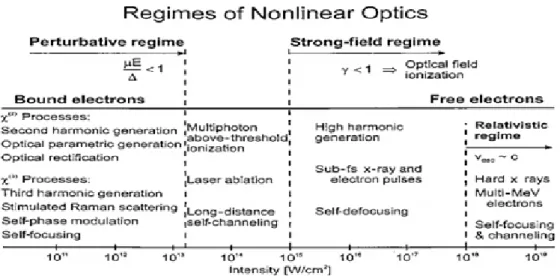
Where Ip the ionization is potential, me is the electron mass and ω is the laser frequency. A perturbative approach [29] is valid if quiver energy is much less than the binding potential, a value of γ << 1 or γ >> 1 indicate the transition lies in the tunneling or multiphoton respectively. Recently, it has been shown two regimes may overlap and are not mutually exclusive [25]. Equation shows γ is dependent on the pulse duration it is likely that tunneling regime can be reached with ultrashort pulse even the below the damage threshold. Figure 4.6 shows different regimes according to the laser intensities used.
Figure 4.6.: Regimes of Nonlinear optics: The defined cut-off boundaries are not sharp and illustrate different nonlinear effect according to laser intensities. In strong field regime, intensities correspond to visible and near-infrared light [25]
.
1
work function of a solid and ionization potential
2
Chapter 4. Generation of Ultra-short pulses: From femtosecond laser to attosecond XUV pulse
4.4. Generation of attosecond pulse: High Harmonic
Generation
There are two methods to break the femtosecond barrier. One is stimulated Raman scattering and the other is to generate attosecond pulse via higher order harmonic gen-eration (HHG). The process which involves the gengen-eration of higher order harmonics their wavefunction lies in the XUV region by focusing of a few cycle laser pulse onto a target. The process was suggested by Paul Corkum in 1933 [30] using semiclassical three step model.
HHG is a process where light of a particular wavelength taken from a solid state laser is converted into a shorter wavelength through non-linear interaction medium. Normally an atomic gas can act as a medium. One can create polarization by displacing the positive and negative charges by oscillating the electric field of the laser pulse. As a result polarization of the medium also oscillates in time and can be expressed as
P (t) = ε0(χ1E1+ χ2E2+ χ3E3+ ...) (4.21)
Here χ1, χ2, χ3 are the linear, quadratic and cubic terms of susceptibilities. In a weal electric field the linear terms dominate but in strong electric field one cannot neglect the higher order terms. Consequently, polarization will contain higher order terms and can be viewed as oscillating dipole that oscillates at integer values n of fundamental frequency ω0. One can achieve extremely short pulse in attosecond regime using such nonlinear process when the pulse laser is tightly focused through the atomic gas. However, for such HHG process one needs to have high power densities on the order of 1013− 1015 W att/cm2 that only can provided by a short pulse laser source (femtosecond regime). On the other hand system that provides such short pulses usually have repetition rate 10 KHz or lower.
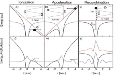
Figure 4.7 shows the classical view of the high harmonic generation process with their quantum mechanical wavefunction at different steps. in In the first step, strong laser field add a potential (marked red) to the unperturbed electron state of coulomb potential. The superposition of the two potential bends down shown . As a result coulomb potential of the valence band become distorted under the influence of the strong laser field (a, d) and electrons can tunnel out of the potential barrier. The free electron become accelerated under the influence of the oscillating laser field (b , e). Finally the electron recombine when the laser field (linearly polarized) changes the direction (c ,f). At the time of recombination an XUV photon pulse is released due to energy gain during the acceleration. Electrons kinetic energy is transferred to the photon as the recollision happens.
Figure 4.8 shows the typical HHG spectrum. Since the pulse is symmetric and electron can release around each peak amplitude, the HHG process will repeat itself at every half cycle. This gives rise to a spectrum of attosecond pulse separated by 2ω. Initially the
Chapter 4. Generation of Ultra-short pulses: From femtosecond laser to attosecond XUV pulse
Figure 4.7.: Classical view is shown in the upper (a,b,c) part, where lower part (d,e,f ) shows the quantum mechanical wavefunction. Electrons tunneling through the barrier (a+d). Accelerated to the laser field (b+e) and very broadband light spectrum due electron recollision with the parent atom (c+f ). [31]
Figure 4.8.: HHG Spectrum. Only odd harmonic has been produced that is separated by twice the frequency [32]
intensity of the harmonic falls, later it stays constant with increasing the harmonic order until a cut-off is reached.
Ecut−of f = IPtarget+ 3.17Up (4.22)
The electron can attain a maximum kinetic energy equal to 3.2 times the pondero-motive potential [33] given by,
Up =
e2E2 4meω2laser
![Figure 2.3.: Formation of bands by broadening the energy levels in a solid [13] (a) Nonde- Nonde-generate energy levels in atomic potential (b) Broadening the energy levels when atoms are closely spaced with each others](https://thumb-eu.123doks.com/thumbv2/5dokorg/5452416.141332/20.892.206.696.130.443/figure-formation-broadening-energy-generate-potential-broadening-closely.webp)
![Figure 2.4.: Bandstructure a of solid (a)reduced (b)periodic(c)extended zone [11]](https://thumb-eu.123doks.com/thumbv2/5dokorg/5452416.141332/22.892.176.722.123.371/figure-bandstructure-solid-reduced-b-periodic-extended-zone.webp)
![Figure 2.6.: Variation in potential energy [14]](https://thumb-eu.123doks.com/thumbv2/5dokorg/5452416.141332/24.892.217.675.575.870/figure-variation-in-potential-energy.webp)
![Figure 3.1.: Photoelectron spectrum as a function of the kinetic energy N (E kin ) of the photoelectron [18]](https://thumb-eu.123doks.com/thumbv2/5dokorg/5452416.141332/27.892.282.627.122.532/figure-photoelectron-spectrum-function-kinetic-energy-kin-photoelectron.webp)
![Figure 3.4.: Photoemission model [18], Three step model in (left) is characterized by transition, scattering and transmission where in one step model is described by the optical coupling between waves inside (Bloch) and outside (plane) the solid.](https://thumb-eu.123doks.com/thumbv2/5dokorg/5452416.141332/33.892.222.674.600.889/figure-photoemission-characterized-transition-scattering-transmission-described-coupling.webp)
![Figure 3.5.: Energy dependent mean free path [20, 21]. Inelastic mean free paths of photoemitted electrons are plotted as a function of kinetic energy.](https://thumb-eu.123doks.com/thumbv2/5dokorg/5452416.141332/34.892.299.590.325.572/figure-energy-dependent-inelastic-photoemitted-electrons-plotted-function.webp)
![Figure 4.1.: Diagram of an ultrashort pulse(8 fs at 800nm) indicating carrier, CEP and envelope [23]](https://thumb-eu.123doks.com/thumbv2/5dokorg/5452416.141332/38.892.251.651.547.850/figure-diagram-ultrashort-pulse-indicating-carrier-cep-envelope.webp)
![Figure 4.3.: Kerr-lens mode-locking(KLM)(a)KLM causes the beam to see greater gain when light intensity is very high, (b) gain and loss dynamics at the center of the beam [26]](https://thumb-eu.123doks.com/thumbv2/5dokorg/5452416.141332/42.892.184.743.154.372/figure-kerr-locking-causes-greater-intensity-dynamics-center.webp)