i THESIS
ADDRESSING ABSORBER QUALITY IN CD1-xMGxTE WIDE BANDGAP SOLAR
CELLS FOR TANDEM APPLICATIONS
Submitted by Carey L. Reich
Department of Mechanical Engineering
In partial fulfillment of the requirements For the Degree of Master of Science
Colorado State University Fort Collins, Colorado
Fall 2018
Master’s Committee:
Advisor: Walajabad S. Sampath James Sites
ii
Copyright by Carey Lucas Reich 2018 All Rights Reserved
ii ABSTRACT
Tandem photovoltaic (PV) solar cells, which use multiple absorbing layers to convert light into electricity, have the potential to surpass the conversion efficiency limits of PV which uses a single absorber. This has been proven using epitaxially grown III-V semiconductors, but these are expensive and are only commonly used for
extra-terrestrial applications. To realize extra-terrestrial, cost effective tandem PV, low cost
production of these highly efficient cells is required. Using absorbers which are similar to cost effective, mass produced PV such as CdTe, Si, or CIGS, this is possible. Si and CIGS have appropriate properties for the IR absorbing layer in a tandem cell, but there is no common PV material with the ideal properties for the UV/Visible light absorbing layer, although CdTe is quite close. Even better, CdTe’s properties can be altered to those of ideal with the addition of ternary elements such as Mg, Zn, and Mn. Issues still remain however as the quality of solar cells produced using ternary alloys of CdTe is much lower than that of the base material. These quality issues seem to stem from the CdTe bulk passivation process, which involves a thermal treatment in the presence of Cl (commonly CdCl2 is used as a source) to passivate the grain boundaries and
catalyze the recrystallization and grain growth process which annihilates detrimental planar crystalline defects in the absorbing material. The work presented in this thesis addresses issues with the absorber quality of solar cells using Cd1-xMgxTe by using
concurrent Cl sources with CdCl2, diffusion barriers during CdCl2, and tweaking the
absorber material with the addition of quaternary elements or novel layers in the device stack. This work culminated in the production of a 10.6% efficient device, a record for
iii
devices using CdMgTe as an absorber, and concludes with paths for future improvements in device performance.
iv
ACKNOWLEDGEMENTS
I would like to thank my advisor, Dr. Sampath for the various opportunities he has made available for me and the incredibly valuable guidance through this research. Without his wealth of knowledge, openness to discussion, and dedication to the improvement of PV technology, the research presented in this thesis would not have been possible. Additionally, I would like to thank Dr. Drew Swanson. He was an inspiration and mentor throughout this work. I owe much of what success I have attained to his willingness to sit down and spend hours discussing the work. Furthermore, Dr. Sites and Dr. Popat for being on my committee and making themselves available for this work. In particular, Dr. Sites allowed me to use his Laboratory for much of the electrical characterization of solar cells presented in this work. I also appreciate the various discussions and help from all lab members in both the PV manufacturing laboratory and the PV characterization laboratory. Dr. Jennifer Drayton in particular has been forthcoming with her wealth of experience and
knowledge. Next, I would like to thank Dr. Holman and his group at Arizona State University for their allowing me to work with their group so closely as I wrapped up the research, which gave me a view of PV from a different technological standpoint. On top of that, I would like to thank Kevan Cameron for his hours of work keeping our
laboratory operating and his mentorship with vacuum equipment. Finally, I would like to thank my friends and family for their support as I moved into graduate studies. I would have been overwhelmed and lost without you. This work was made possible by
v
funding from the NSF I/UCRC under award number: 1540007and DOE PVRD under award number: DOE PVRD DE-EE0007552
vi
TABLE OF CONTENTS
ABSTRACT ... ii
ACKNOWLEDGEMENTS ... iv
TABLE OF FIGURES ... viii
1) Introduction ... 1
1.1) Climate Change ... 1
1.2 )Renewable Alternatives ... 3
1.3) Solar Energy ... 4
1.3.1) Characterization of a Solar Cell ... 12
1.3.2) Thin Film Solar PV ... 14
1.3.3) Tandem/Multi-junction Solar Cells ... 15
1.3.4) CdTe-Based Wide Bandgap Materials for Multi- Junction Solar Cells ... 17
2) Necessary Change of Device Electron Contact ... 20
2.1) Materials and Methods ... 20
2.2) Results and Discussion ... 21
3) Use of Magnesium Chloride for Passivation of CdMgTe ... 27
3.1) Materials and Methods ... 27
3.2) Results and Discussion ... 28
4) Chloride Mixture for Passivation of CdMgTe ... 32
4.1) Materials and Methods ... 32
vii
5) Cadmium Sulfide Capping Layer... 40
5.1) Materials and Methods ... 40
5.2) Results and Discussion ... 41
6) Conclusions and Future Work ... 49
viii
TABLE OF FIGURES
1.1.1) Atmospheric CO2 Measured at Mauna Loa ... 2
1.2.1) Available Energy Resources ... 4
1.3.1.1) Energetic differences between insulators, semiconductors, and conductors ... 6
1.3.1.2) Schematic of intrinsic and doped Si ... 8
1.3.1.3) JV and power curves for a CdTe device from CSU ... 10
1.3.1.4) Limiting efficiency and JV parameters for single junction solar cells ... 12
1.3.4.1) Energy usage in the AM1.5 spectrum of 1 junction vs multijunction PV ... 16
2.1.1) CdMgTe device structures used... 21
2.2.1) XRD of CdMgTe films deposited on CdS vs MgZnO ... 23
2.2.2) JV of CdMgTe devices deposited on CdS vs MgZnO ... 24
2.2.3) EQE of CdMgTe devices deposited on CdS vs MgZnO ... 25
2.2.4) TEM and EDXS of and as deposited CdMgTe film on MgZnO ... 26
3.2.1) JV of a CdMgTe device passivated using the University of Liverpool MgCl2 recipe ... 29
3.2.2) JV of the best performance MgCl2 passivated CdMgTe device ... 30
3.2.3) EQE of a CdMgTe device passivated with MgCl2 ... 31
3.2.4) PL of a CdMgTe device passivated with MgCl2 ... 31
4.1.1) Schematic of the MgCl2 and CdCl2 mixture passivation tool ... 33
4.2.1) JV of the best performing device passivated with CdCl2 and MgCl2 ... 34
4.2.2) PL of CdMgTe films passivated with CdCl2 and the mixture with MgCl2 ... 35
ix
4.2.4) Transmittance of an as deposited CdMgTe film and a CdMgTe film passivated with the mixture of CdCl2 and MgCl2 ... 38
4.2.5) EQE of a CdMgTe device passivated with the mixture of CdCl2 and MgCl2 ... 39
5.2.1) JV of CdMgTe devices of varying CdCl2 anneal duration with a CdS diffusion
barrier ... 42 5.2.2) EQE of CdMgTe devices of varying CdCl2 anneal duration with a CdS diffusion
barrier ... 43 5.2.3) Device structure with the addition of CdSeTe between MgZnO and CdMgTe .... 44 5.2.4) JV of CdSeTe/CdMgTe devices ... 45 5.2.5) EQE of CdSeTe/CdMgTe devices ... 46 5.2.6) TRPL of CdSeTe/CdMgTe devices ... 48
1
1) INTRODUCTION
1.1) Climate Change
The planet earth is experiencing dramatic changes to its climate, with the main driving force being the emission of greenhouse gasses from human activities [1]. Many sources of these emissions exist, such as the emissions of methane and CO2 from
cattle grazing and breakdown of organic waste in landfills, but the major source is from the burning of fossilized organic compounds (fossil fuels) to convert the energy stored within into a form useful to humans, often in the form of kinetic energy in the
transportation sector or electricity in the power sector [2].
The reason that these emissions are causing climate issues is because the rate at which CO2 and other greenhouse gasses are being emitted is greater than the rate
they can be naturally removed from the atmosphere. This has increased the
concentration of them in the atmosphere, and continues to push the concentration ever higher[3]. This record has been tracked by the Mauna Loa observatory in Hawaii and the CO2 concentration since 1950 can be found in figure 1.1.1 [3]. Unfortunately, this is
due to human emission primarily, as natural fluctuations since we have been able to extract measurements of them from polar ice have always remained relatively low, below 300 PPM in the atmosphere. Since the industrial revolution and the widespread human burning of fossil fuels this number has risen significantly, recently passing 400 PPM at the annual low [4].
This is problematic because the earth relies on radiation to emit excess thermal energy, with the primary emission being in the IR [5]. Greenhouse gasses absorb
2
strongly in the IR, and thus do not allow the necessary emission of thermal energy to maintain a stable environment (conversely, if the concentration of greenhouse gasses becomes too low the earth would emit too much thermal energy in the form of IR light, but this is not the current issue)[5].
Figure 1.1.1: Mauna Loa observed atmospheric CO2since the lab’s creation. [3]
It has been predicted by climate scientists that the average global temperature must be maintained at less than 2°C above the historical average to avoid the worst effects of climate change, and potentially to avoid run-away warming [6]. Recently, the average global temperature reached ~1 °C above the historical average, and the rate at which the temperature is increasing is also increasing [7]. In order to avoid reaching 2
3
°C, it is imperative that emission of greenhouse gasses is dramatically reduced in the near future [6]. While multiple sources of these emissions exist, movement toward a renewable energy economy will be a step toward this goal.
While some progress has been made toward use of alternative energy
conversion techniques, human reliance on conventional sources of energy is deep and far reaching. In the US, the electric generation industry has the deepest penetration of non-fossil fuel energy sources, at nearly 17% in 2017 [8]. The remaining 83% was then responsible for greater than 99% of the industry’s CO2 emissions which totaled to 1744
metric tons, which was only a third of the US CO2 emissions that year [8]. This obviously
implies that there are other issues which much be addressed, namely transportation, but increased penetration of electric vehicles has the potential to move the bulk of greenhouse gas emissions into the electricity industry [8].
1.2) Renewable Alternatives
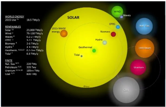
A variety of alternatives to replace traditional (fossil fuel burning) production are known. In nearly any situation where the targets in reduction of emissions are to be met, energy production must be met with a variety of these, using the optimal source for the region [8]. However, of all renewable sources, only solar and wind energy have the potential to entirely power the world’s energy needs[9]. Additionally, as seen in Figure 1.2.1, solar power has the potential to produce well more than the world energy needs, and in a year could produce more useful energy for humans than the total availability of known fossil fuel reserves remaining [9].
4
Figure 1.2.1: 2015 estimates of energy resources, non-renewable sources show recoverable reserves and renewable sources show annual resource. The total energy use worldwide during 2015 is shown as a reference for magnitude of resource
availability [9] 1.3) Solar Energy
As Solar energy shows the greatest potential, understanding the production techniques is essential, and there are two main energy conversion techniques for converting the sunlight to usable energy: Solar PV and Solar Thermal. Solar Thermal uses concentrators to heat a substance, then use that heat to produce electricity [10]. This is generally achieved by using a molten salt to absorb the heat energy and then using the hot salts to boil water and produce electricity by expanding the water vapor through a turbine similar to coal or nuclear power production [10]. However, this thesis
5
will focus on production using solar PV production, wherein sunlight is directly converted to electrical power.
1.3.1) Basics
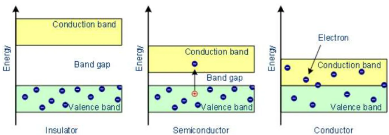
Solar PV uses unique properties of semiconducting materials to produce electricity. A semi-conductor is a material with electrical properties between that of a conductor and that of an insulator. The difference between these materials can be understood from an energetic perspective: how much energy does it take to move a charge carrier in a material? In conductive materials, the energy requirements are low, as often electrons in the valence shell of an atom are fairly free to move between atoms. In an insulator however, some relatively large amount of energy is required to move an electron away from the valence of an atom[11].
Due to the nature of atoms, each shell of electrons may exist at a specific energy level. When bonded however, electrons in the valence shell sit at a variety of energy states, which is called the valence band [11]. The energy required to move an electron throughout a material is seen as the amount of energy needed to excite an electron to an energy state where it can no longer sit in the valence band of energy states [11]. Due to the quantum nature of electrons, an electron cannot exist at an energy state greater than the maximum allowed state in the valence band and less than the minimum energy state allowed for a free electron in a material [11]. This creates a new energy “band” of states at or greater than the minimum energy state required for an electron to be free, called the conduction band [11].
When seen this way, conductors often have close to- or overlapping valence and conduction bands, and the energy difference between the valence band and conduction
6
band is quite large in an insulator[11]. A semi-conductor then has a bandgap (the difference in energy between the valence band maximum and the conduction band minimum) which is greater than a conductor, but less than an insulator. A visualization of this can be seen in Figure 1.3.1.1.
Figure 1.3.1.1: Visualization of bandgap differences between insulators, semiconductors, and conductors. [11]
The reason semiconductors are ideal for the solar PV application is that electrons in the valence band can be excited to the conduction band where they are mobile by absorbing light [12]. Specifically, their middle ground bandgaps allow for absorption in the solar spectrum, as an insulator would likely behave in much the same way but the energy requirements to do so are too great for excitation from the solar spectrum [12]. This effect is possible because incident photons of an energy at or greater than the bandgap of the material will donate their energy to an electron to excite it [12]. The remaining photons with too little energy to do so are transmitted then through the material as they did not carry enough energy to excite any electrons all the way to the conduction band [12].
7
This alone however is not enough to make a solar cell. It will however make a great photo-sensor, as the current through a semiconductor with a given applied bias would increase with incident light greater than the bandgap energy due to the increased number of electrons in the conduction band [12]. In order to generate electricity, a driving force for the free electrons to move has to be internally available. This is
generated using doping of the semi-conductor to make a junction between a p-type and n-type semiconducting material [12].
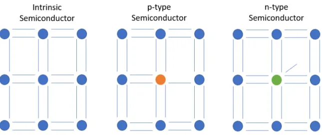
A p-type semiconductor has an excess of positive charge carriers known as holes, in essence a missing electron from the valence of an atom [12,13]. On the other hand, n-type semiconductors have an excess of negative charge carriers, electrons [12,13]. This is achieved by the addition of atoms with a different valence than the semiconductor [12,13]. An easy example can be made using Si, the most commonly used semiconductor. A single silicon atom has 4 electrons in its valence shell, but when bonded in pure Si, electrons are shared with 4 other silicon atoms, filling the valence shells to full with 8 electrons. In a Si material that is doped p-type, nearly all of the Si will be in the same configuration as the un-doped case. However, some of the Si atoms will be bonded to 3 other Si atoms and one atom with a valence containing 3 electrons. This will then leave the bonds of these atoms missing a single electron (a hole). In Si this is usually achieved through the addition of boron [12,13]. An n-type Si material is much the same except the added atom has a valence of 5 rather than 3 or 4, therefore donating an extra electron, and this is often achieved through the addition of phosphorous or arsenic [12,13]. This can be visualized in Figure 1.3.1.2.
8
Figure 1.3.1.2: a) intrinsic Si b) a p-type dopant in a Si matrix (orange, unsatisfied bond seen in the missing line) b) an n-type dopant in a Si matrix (green, extra electron seen in the extra line). Note that this visualization assumes the unseen bonds of the exterior atoms are fully satisfied.
When taking a p-type and an n-type material and putting them in intimate contact, a p-n junction is formed [12,13]. In this formation, a region directly at and adjacent to the contact will have the excess electrons and holes inter-diffuse to
annihilate each other (the excess electrons fill the holes) [12,13]. This however leaves an unbalance in charge, as the number of protons in the nucleus of the dopant atom remains unchanged. As such, the p-type material, which is gaining electrons, will gain a negative charge from the extra electron than protons per dopant atom, and the n-type material which is losing the electrons will gain a positive charge from one less electron than protons per dopant atom [13]. As more holes and electrons diffuse and annihilate, the charged region will grow stronger until the electrons and holes are repelled and can no longer diffuse across the charged region, called the space charge region or depletion region [12,13]. At this point one has a diode, where no current will flow unless an
9
applied bias provides enough energy for electrons and holes to cross the charged region [13].
In this configuration, the last step is then to shine light which will be absorbed onto the material [12]. If an excited electron or hole from the incident light is in the space charge region either from local excitation or drifting in, the field will force the charge carrier to one side or the other, producing current through the diode [12]. This current opposes the current which would be produced by applying a bias as one would across a standard diode, allowing the production of power rather than the consumption [12]. As a bias is applied under illumination, the current produced by photonic excitation of
electron hole pairs will flow, but will start to be opposed by the current produced by the applied bias once this provides enough energy to move electrons across the space charge region [12]. The photo generated current eventually be overcome as great enough current is supplied by the bias [12].
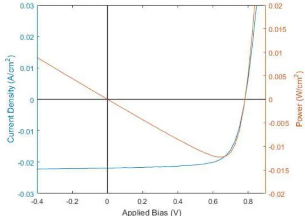
When plotted as current density vs applied voltage, this behavior stemming from the illumination of a p-n junction with appropriate properties appears as a diode curve with an offset by the amount of current produced by the illumination, as seen in Figure 1.3.1.3. From this curve one can extract the necessary parameters to calculate the solar cell efficiency (given a known power of the illumination). First is the short circuit current which is roughly equivalent to the photo generated current occurs when a bias of 0V is applied to the cell [12]. Next is the open circuit voltage, which is the applied bias
required for the production of a diode current of the same magnitude of the
photocurrent, resulting in a net current of 0 Amperes [12]. This is clearly seen at the location where the JV curve crosses the X axis. Finally, as voltage is applied, a
10
maximum power point is achieved as visualized by the power curve in Figure 1.3.1.3. at this point a fill factor is extracted, which is a ratio representing the squareness of the diode curve [12]. This is defined as the power at the maximum power point to that of the power which would be produced if the solar cell could operate at short circuit current and open circuit voltage simultaneously [12]. These numbers are calculated simply using the relationship that electrical power is equal to the product of the current and the voltage. Efficiency of the solar cell is then the ratio of the product of the open circuit voltage, the short circuit current, and the fill factor to the illumination power [12].
Figure 1.3.1.3: JV and power curves of a CdTe solar cell produced in CSU’s PV manufacturing laboratory.
If one recalls the bandgap discussion, one can infer that solar cells from different materials with different bandgaps will behave differently. This is true, and there is
11
actually a great difference in achievable efficiency with semiconductors of different bandgaps[14]. A narrower bandgap will allow for absorption of more photons, and thus a solar cell of this material will produce more current[14]. However, a solar cell with a wider bandgap will achieve higher voltages due to the greater energy difference carried by the electrons in the conduction band and holes in the valence band, leading to a trade off with a maximum bandgap for conversion efficiency of a solar cell [12]. Due to spectral variation in the AM1.5G solar spectrum, which is the standard spectrum for testing solar cells, two roughly equivalent peaks occur with bandgaps of ~1.1 eV and ~1.4 eV with the efficiency around 33% maximum [14]. This analysis is represented as efficiency as well as JV parameters in Figure 1.3.1.4, which is from Russell Giesthardt. Solar cells of this type are fast approaching their practical limits which are some number slightly below the theoretical maximum[14].
12
Figure 1.3.1.4: Theoretical maxima of single junction solar cell JV parameters under AM1.5 illumination [14]
1.3.2) Characterization of a Solar Cell
In order to diagnose losses in efficiency, solar cell characterization is quite
important. Previously, extraction of efficiency from Jsc, Voc, and FF have from a JV curve
has been covered. Additionally, various other parameters can be extracted. First, the linear portions of the derivative of the curve can be used to determine the series and shunt resistances in the cell [12]. Additionally, non-exponential behaviors such as bends in the curve can be indicative of poor contacts [12].
Another important measurement is the external quantum efficiency [12]. This is the ratio of carriers collected to incident photons, resolved by wavelength or energy of incident photon [12]. In this measurement, one can determine the bandgap of the
13
material by what wavelength at which the solar cell stops collecting carriers [12]. Additionally, it can be paired with transmission, reflection, and other optical
measurements to determine what the losses in current collection are [12]. Additional losses from those optically determined are generally attributed to recombination of minority carriers prior to collection [12]. A solar cell with a low density of defects which act as recombination centers will approach the limits determined by the optical losses, but a defect-dense solar cell will show external quantum efficiencies below the optical limits [12]. This is because the minority carriers will recombine before they are collected in such a solar cell.
Another measurement essential to characterization of solar cells, particularly thin film solar cells, is photoluminescence (PL) and the closely coupled time resolved
photoluminescence (TRPL) [15]. These measurements give valuable information about charge carrier behaviors in the absorber. For example, the intensity should correlate to the fraction of radiative recombination in the absorber, giving an idea of how
recombination prone the material is. Meanwhile, TRPL measures the radiative
recombination decay after a brief excitation, giving an idea of carrier dynamics in the absorber [15]. The decay can be used to extract the minority carrier lifetime and often is in thin film PV [15]. Silicon PV has other, simpler measurement techniques to determine lifetime, but these will not be covered in this thesis.
On the material side of the characterization spectrum, X-ray diffraction (XRD) is used to assess crystallinity. In this measurement, the sample is irradiated with
columnated X-rays, and then the angle of incidence and the angle of the detector are swept [16]. At certain angles, the incident X-rays will be diffracted and collected by the
14
detector [16]. Which angles this occurs at indicates the crystal structure of the film as defined by Bragg’s law, and each angle with a diffraction peak is indicative of a family of crystallographic planes in the material [16]. From XRD data, a simple calculation based on the Bragg relationship can be used to determine the planar spacing and therefore the lattice constants of the material’s crystal structure [16]. A lack of peaks observed can be indicative of an amorphous material, which has no regular crystal structure.
Finally, Transmission Electron Microscopy (TEM) and energy dispersive X-ray spectroscopy (EDXS) are used for material characterization. In TEM measurements, an electron beam is focused on a thin sample and transmitted electrons are then collected and form an image [17]. Due to the short wavelength of electrons, the images created by these transmitted electrons can show down to nanoscale features of the materials being measured [17]. In EDXS, these same electrons from the TEM are used for material analysis. Incident electrons of high energy can excite core shell electrons of atoms [18]. Some portion of these electrons decay to their original shell and during this process emit photons in the X-ray spectrum [18]. Specific wavelengths of X-ray
correspond to certain transitions in specific materials as the emitted photon is at the energy level of the energy transition made in the decay, and thus elemental analysis is possible through measurement of emitted X-ray spectra during electron microscopy [18].
1.3.3) Thin Film Solar PV
Si PV, the most common on the market, is complex to manufacture, and uses 100x the semiconducting material as thin film technologies [19]. As this thesis focuses on the use of CdTe-based thin film PV, CdTe will be used as a comparison.
15
Like most thin film technologies, CdTe is manufacturable at the large scale quite simply using established thin film deposition techniques which are used heavily in industry today. For example, First Solar, the largest PV manufacturer in the US, uses a vapor transport deposition methodology [20]. These techniques allow for fast, low-cost production of high efficiency, stable solar modules.
Additionally, the bandgap of CdTe is direct, with strongly absorbing behavior in the wavelengths with energy greater than the bandgap [21]. This allows as little as 1 micron thick devices to absorb 99% of the usable photons, although most devices are 2-8 microns thick [22]. This is still ~100X less material used than a Si PV cell of the same area, as silicon’s poor absorption behavior due to its indirect bandgap requires a greater thickness to absorb the same amount of useful light [19]. Between the use of 100X less semi-conductor and simple manufacturing techniques, thin film PV can be a lost-cost alternative to the traditional silicon solar [19].
1.3.4) Tandem/Multi-Junction Solar Cells
Previously some analysis from Russell Giesthardt was shown with theoretical limiting efficiencies for solar cells of different bandgaps [17]. It is possible to surpass these theoretical maximum efficiencies if a solar cell is produced with more than one absorber [23]. This is possible due to the absorption nature of semiconductors and the trade off with bandgap. Because photons with less energy than the bandgap of the material are transmitted in a semiconductor, a wider bandgap solar cell with transparent electrical contacts can be placed over a solar cell with a narrower bandgap, and both will be producing power [23]. While the two can operate on separate circuits, it is expected to be favorable for installation to wire the two in series to reduce hardware
16
costs [23]. This is called “two terminal” and has additional limitations. Primarily the current will be limited by whichever of the two or more sub-cells is producing less current [23]. This leads to bandgap optimization of the two sub-cells being essential to attaining the greatest possible efficiencies by matching the current produced by the sub-cells [23].
While the current will be lower than the lower bandgap sub-cell’s stand alone current would be, the efficiency will be greater from these cells for a few reasons. First, at the device measurement level, the voltages will sum in the series configuration producing higher voltages than possible with the same current for the widest bandgap sub-cell (recall that a wider bandgap will allow for the production of a device with greater voltage, at the expense of current collection). A solar cell is also sensitive to
temperature, as the thermal energy will reduce the energy requirements for the diode current to flow, reducing the open circuit voltage [12]. This effect is found in the term J0,
or the reverse saturation current, in the diode equation as temperature increases, which will increase the forward current and thereby reduce the bias needed to produce an equal current to the photocurrent, reducing Voc [12]. When photons of energy far greater
than the bandgap are absorbed, the excited electron hole pair quickly decays to the CBM and VBM, with the excess energy released during that decay being in the form of heat energy [12]. In the tandem configuration, thermalization losses will be greatly reduced due to absorption of high energy photons in a wider bandgap material. This will allow for greater voltages to be obtained by both the sum of voltages in series and the reduction of voltage losses due to thermalization. The difference between a single junction’s potential energy usage of the solar spectrum and a 3 junction solar cell’s
17
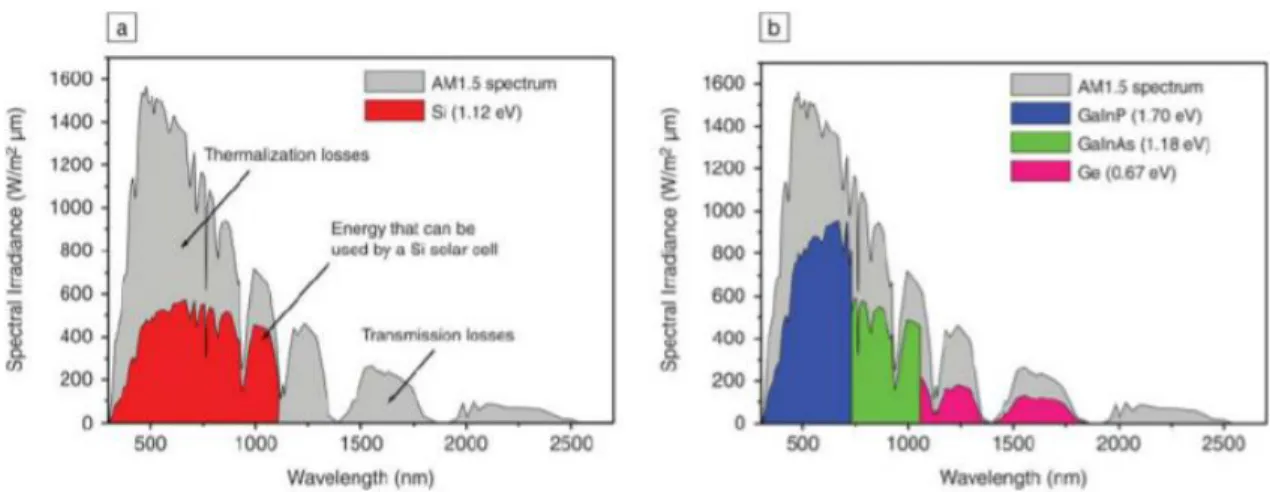
usage can be seen in Figure 1.3.4.1. with losses identified, which is taken from [24]. Note that the region attributed to thermalization losses is reduced from the Si plot to the multijunction plot, as well as a greater portion of the spectrum can be converted.
Figure 1.3.4.1: Energy conversion possible by a) a silicon solar cell and b) and 3 junction solar cell relative to the energy resource (AM1.5 spectrum in gray) with cell losses identified. [24]
CdTe-Based Wide Bandgap Materials for Multi-Junction Solar Cells
As previously noted, in order to produce high efficiency tandem solar cells, a wide bandgap absorber layer needs to be used in one junction and a narrow bandgap layer needs to be used in another physically behind the wide bandgap layer with
reference to the incident photons. Modelling shows that for a series constrained device, the bottom cell bandgap can be optimal at around 1.1 eV [23]. Absorbers with mature manufacturing and technology bases exist for this narrow bandgap layer, such as Si and the thin film solar cell material Copper Indium Gallium di-Selenide (CIGS) [23].
However, no absorber is currently mature or high performing enough for the top cell at the optimal bandgap. This leaves space for technological development of a
low-18
cost, high efficiency solar cell at this bandgap. As previously mentioned, production of CdTe is low-cost and produces high-efficiency cells. It should then be possible to leverage the existing CdTe production to produce wide bandgap top cells in the same manner if they are CdTe-based, and luckily, multiple options for tuning the bandgap of CdTe based semi-conductors to that of ideal for tandem PV top cells exist.
Addition of Mg, Zn, or Mn in to the CdTe lattice will increase the bandgap from 1.5 eV. This is done by forming a matrix of CdTe and MgTe, ZnTe, or MnTe in the form of Cd1-xYxTe wherein Y is Mg, Zn, or Mn [22-24]. For all of these a bandgap of 1.7 eV,
modelled to be ideal for two terminal tandem devices with the 1.1 eV bottom cell, can be achieved with x<1 [25-27].
These materials have yet to produce high performance solar cells at 1.7 eV bandgaps. This is believed to primarily be due to the instability of the alloy during the CdCl2 passivation step used to increase the absorber quality for poly-crystalline CdTe
devices. During this process, an anneal in the presence of CdCl2, CdTe devices can go
from <1% efficient to 20%+ assuming that an appropriate device structure is used [28-30]. This is achieved by a few effects. First, the grain boundaries (GBs) are decorated with Cl, which then sits in Te vacancies, eliminating this dangling bond and reducing the GB defect density [28-30]. In addition to the Cl at the GBs, the process acts to promote recrystallization and grain growth [28-30]. During this process planar defects such as stacking faults are removed, and twin boundaries remain, but appear benign to solar cell performance [28-30].
However, when the alloys are subjected to this process, the primary effect is the reduction of the ternary elements, reducing the material to CdTe [31-33]. Favorable
19
reactions with CdCl2 have been identified previously as likely culprits for the loss [34].
Specifically the favorable reaction in equation 1 is expected to be the culprit so long as excess O2 and H2O are removed from the environment during processing [34].
Overcoming these issues during the passivation process for CdMgTe is the focus of this thesis, with some additional considerations to device structure.
20
2) NECESSARY CHANGE OF DEVICE ELECTRON CONTACT
Traditionally, CdTe solar cells have been manufactured with a CdS hetero-junction partner, and thus the initial configuration used for CdMgTe was to simply
replace the CdTe layer in the traditional structure. This lead to a poor interface between the CdS layer and the CdMgTe layer which was prone to delamination during CdCl2
processing. This section will address the issues with the CdS layer and the alternative which was transitioned to.
2.1) Materials and Methods
The final device structure using CdS is found in Figure 2.1.1. This involves a 3.3 mm thick soda-lime glass (SLG) superstrate, commercially available with a transparent conducting oxide (TCO) pre-deposited. The specific glass used was Pilkington TEC12D. On the TCO, 125 nm of CdS was deposited using a Close space sublimation (CSS) technique. After this layer, the absorber was deposited directly. For this deposition, the technique used was a modified CSS deposition called co-sublimation. This previously developed methodology in the Photovoltaic Manufacturing Laboratory at Colorado State University, takes advantage of favorable formation energies for the alloys deposited [34]. For example, the reaction with Mg and CdTe is favorable at 400 °C Celsius to form MgTe [34]. In sublimating Mg and CdTe at the same time, the reaction is allowed to progress, and the alloying content is controlled by the relative fluxes of CdTe and Mg. The target bandgap was 1.7 eV and the layer thickness was 1.5 microns. A MgCl2 and
CdCl2 simultaneous passivation process to be discussed in depth in the Chloride
21
previously described Cu doping process was used [35]. Finally, a bilayer of carbon and nickel in a polymer binder is applied through a spray application as an electrode.
Figure 2.1.1: a) device structure using CdS b) device structure using MZO
For the alternative to CdS, recent developments in the CSU PV Manufacturing Laboratory had shown a layer of Zn1-xMgxO (MZO) was a viable replacement for the
traditional CdS, with the benefit of increased transparency producing more current [36]. This layer is optimized for CdTe, but viable to use with a wider bandgap material. At CSU it is deposited using planar magnetron sputtering with an RF power of 180 W in an environment of 5 mTorr, composed of 97% Ar and 3% O2.
XRD measurements were taken on a Bruker AXS D8 thin film XRD measurement system in the Bragg Brentano configuration (θ/2θ). 2θ was swept from 10 to 80° with a step size of 0.02°. TEM and EDXS samples were prepared using Focus Ion Beam (FIB) milling using a dual beam FEI Nova 600 Nanolab. A standard in situ lift out method was used to prepare the cross section. A platinum overlay was deposited on the free surface of the film to define the area of interest on the surface of the sample, homogenize the final thinning of the sample and to avoid damage from the ion beam. STEM images are collected using a FEI Teenai F20 (S)TEM operating at 200 kV.
22 2.2) Results and Discussion
Immediately after the chlorination process for samples with CdS, delamination was observed, although some areas of adhesion were remaining. To identify where the delamination issues were occurring a peel off method was used with transmittance measurements to verify the delaminated layer. A cloth was dipped into an epoxy layer applied to the film side of the sample. This was immediately set by dipping the sample in liquid nitrogen and removed by pulling on the cloth. This was done prior to formation of the device and so the only layers on the glass were the TCO, CdS, and CdMgTe. Therefore, a transmittance measurement will determine the location of the delamination so long as it is not between the glass and TCO. Luckily, the glass had a yellow layer remaining suggesting CdS, which was confirmed using a transmittance measurement which showed the bandedge to be near 525 nm.
In an attempt to avoid delamination problems, a 100 nm MgZnO layer was used in place of CdS, with a TEC10 superstrate rather than the TEC12D superstrate used with CdS. Using this structure, seen in figure 2.1.1, and subject to the same chlorine treatment, no delamination was observed, showing that MgZnO was an effective replacement for the CdS to solve adhesion issues during CdCl2.
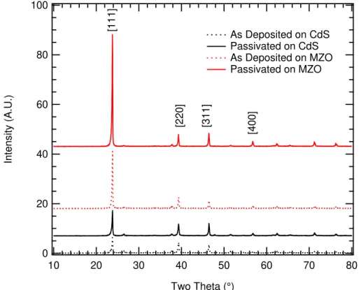
Additional differences between the CdMgTe layers as deposited on the different window layers were noted, both in final device performance and material properties. X-ray Diffraction (XRD) measurements revealed a difference in the crystalline nature of CdMgTe as deposited. The XRD can be found in figure 2.2.1. The relative peak heights indicate that with CdS, the [111] family of planes shows some preference, and this is much stronger for the CdMgTe on MZO. Also shown is the XRD measured of films after
23
CdCl2 which showed the least degradation of composition. This measurement shows
that on CdS, the preferred orientation is relatively unchanged after CdCl2 with a small
increase in the [111] peak intensity, while on MZO the preference for the [111] planes increased dramatically.
Figure 2.2.1: XRD spectra of CdMgTe (CMT) deposited on CdS and MZO before and after passivation
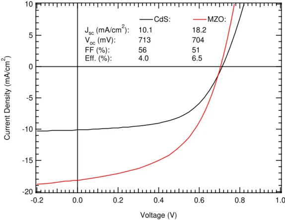
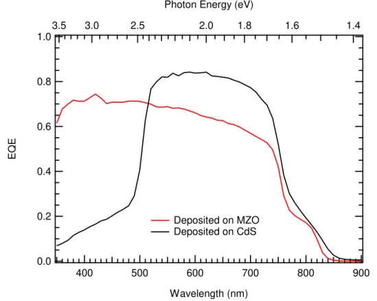
Current Density vs Voltage measurements are found in Figure 2.2.2. One of the motivations for developing MZO as a replacement for CdS in the CdTe community was to eliminate the parasitic absorption due to the narrower than ideal bandgap for a window layer of CdS at ~2.25 eV, which limited the current collection from the CdTe. MZO, with a tunable bandgap greater than 3.5 eV, is transparent to photons of these wavelengths and therefore increased the current collection and as a result the efficiency of the device. This same effect is seen in the CdMgTe devices, which saw a 2%
100 80 60 40 20 0 Int en s ity ( A .U.) 80 70 60 50 40 30 20 10 Two Theta (°) [111] [220] [311] [400] As Deposited on CdS Passivated on CdS As Deposited on MZO Passivated on MZO
24
absolute increase in efficiency from the use of MZO rather than CdS. This effect is nearly entirely accounted for in the increase in current collection as the there was a non-negligible reduction in fill factor. The External Quantum Efficiency in Figure 2.2.3
confirms that this is due to a reduction in parasitic absorption below ~530 nm.
Figure 2.2.2: Current Density vs Voltage measurements for CdMgTe solar cells deposited on CdS and MZO.
While the MZO eliminated delamination issues, other issues remain. First of all, the MZO used in this study was optimized for the narrower bandgap material CdTe, and therefore the band alignment of the CdMgTe with the MZO is likely less than ideal. For CdTe, the band alignment with MZO is a critical aspect of the contact. It has been demonstrated that the optimal MZO for use with CdTe has a 0.2 eV positive conduction band offset. By increasing the bandgap with the addition of Mg, it is estimated that some
-20 -15 -10 -5 0 5 10 Cur ren t Den s ity ( mA /c m 2 ) 1.0 0.8 0.6 0.4 0.2 0.0 -0.2 Voltage (V) CdS: MZO: Jsc (mA/cm2): 10.1 18.2 Voc (mV): 713 704 FF (%): 56 51 Eff. (%): 4.0 6.5
25
portion of the increased bandgap is from pushing the conduction band closer to vacuum level (anywhere from 50% to 70% of the change in bandgap, as discussed by Pavel Kobyakov in his PhD Dissertation), therefore reducing this optimal CBO [34].
Figure 2.2.3: External Quantum Efficiency of CdMgTe solar cells deposited on CdS and MZO
In addition to altering the band alignment, analysis of devices in this structure in a transmission electron microscope (TEM) using energy dispersive X-ray spectroscopy (EDXS) to locate the elemental composition show interdiffusion of Mg and Zn between the absorber and the bulk in the as deposited films. This analysis is shown in Figure 2.2.4, and clearly shows Zn (in purple) entering the bulk, and diffusing through along the GBs while Mg depleted regions of the bulk are seen in close proximity to Mg rich and Zn deficient regions of the MZO, which is observed to be of uniform composition in CdTe
1.0 0.8 0.6 0.4 0.2 0.0 E Q E 900 800 700 600 500 400 Wavelength (nm) 3.5 3.0 2.5 2.0 1.8 1.6 1.4
Photon Energy (eV)
Deposited on MZO Deposited on CdS
26
devices. This effect can alter the contact properties from uniform, and the effect of which on device performance is unknown.
Figure 2.2.4: TEM and EDXS of an as deposited CdMgTe cell on MZO showing interdiffusion of Zn and Mg. TEM imaging and EDXS mapping were carried out by Ali Abbas at Loughborough University in Loughborough, UK.
In spite of the known issues with the MZO window layer, the apparent fix of the delamination issue, increased current collection, and availability in the CSU PV
manufacturing laboratory gave enough motivation to change from CdS to MZO for subsequent investigations of CdMgTe solar cells.
27
3) USE OF MAGNESIUM CHLORIDE FOR PASSIVATION OF CDMGTE
The traditional source of Cl for passivation of grain boundaries is CdCl2. This
material is however problematic for the passivation process with CdMgTe, as the favorable reaction between MgTe and CdCl2 yields CdTe and MgCl2, thereby reducing
the alloying content of the semiconductor [34]. This change in composition effectively reduces the bandgap from the as deposited film and the desired bandgap for tandem applications to that of CdTe [34]. Work from the University of Liverpool has shown that MgCl2 can be used with CdTe to achieve similar results to CdCl2 [37]. Replacement of
CdCl2 with MgCl2 in the passivation of CdMgTe, the energetics of the previously
mentioned reaction would imply that no change in alloy content should occur. In this section MgCl2 passivation processes are investigated to mitigate loss of ternary
elements during the chlorine passivation process step. 3.1) Materials and Methods
The device structure in this section is the same as the MZO contact structure in the previous section, with a 2 micron thickness for the absorber layer. This structure can be found in figure 2.1.1 of the previous section and is composed of TEC10 glass, MZO, the CdMgTe absorber with a chlorination process and a Cu doping process, a Te contact, and a painted carbon and nickel electrode [35].
The MgCl2 processes used are adapted from the work at University of Liverpool.
First, the process was replicated. This involved the spray application of a 1M MgCl2
solution purchased from Alfa Aesar to soda-lime glass until coverage was uniform. Next, the sample was placed on the source plate with 3 mm SLG spacers. This stack of
28
source and sample was then placed in a tube furnace, which then was evacuated and backfilled with 99.999% pure N2 from Airgas. This environment is a change from the
Liverpool recipe, but as it is known that CdMgTe can form detrimental MgO at the surface when in the presence of O2, contributing to compositional changes, the pure N2
environment was selected [34,37].
Next, the process was varied in environment, duration, and temperature. The temperature was varied between 410°C and 510°C, the duration between 2 minutes and an hour, and the use of a 98% N2 and 2% O2 environment was investigated. The
addition of some oxygen was used following some analysis suggesting that the vapor pressure and therefore flux of MgCl2 at the process temperatures used is minimal and
O2 in the environment should react with MgCl2 to form MgO and Cl2 at the temperatures
used in the process. In this case, the Cl2 gas product of the reaction would be
responsible for the chlorine passivation, a process for which there is demonstrated potential with CdTe.
3.2) Results and Discussion
The JV characteristics can be seen in Figure 3.2.1 for the replication of the Liverpool work for CdMgTe. As seen, the performance of the solar cell is poor, with an efficiency below 1%. In the power production quadrant (IV) the device appears to behave much like a resistor, a diagonal line. This indicates poor absorber properties, and poor diode formation, likely as a result of the absorber remaining of poor quality.
29
Figure 3.2.1: JV of a CdMgTe cell passivated with a replication of the process used at the University of Liverpool
JV and EQE curves can be found in Figures 3.2.2 and 3.2.3 respectively for the device with the best performance from all of the MgCl2 passivation experiments. This
device was the result of a 40 minute anneal at 430°C in an environment of the mixed nitrogen and oxygen gas. It is shown that efficiency is less than 1% due to low current, voltage and fill factor. This indicates that the passivation process was not successful.
-20x10-3 -15 -10 -5 0 5 Curr en t Den sity (A/cm 2 ) 1.0 0.5 0.0 -0.5 Voltage (V) Voc: 405 mV Jsc: 5 mA/cm2 FF: 23.3% Efficiency: 0.47%
30
Figure 3.2.2: JV characteristic of the best performing MgCl2 Vapor processed device
In Figure 3.2.4 a measured PL spectrum from the device with the greatest JV performance is shown. This device has negligible PL signal. This is also indicative of an ineffective passivation process.
It is possible that the MgCl2 passivation process is ineffective due to the low
vapor pressure at temperatures low enough to avoid re-sublimation of CdMgTe from the glass. Data from the CRC handbook indicates that in order to achieve comparable vapor pressures to the standard CdCl2 used in the CSU PV manufacturing laboratory,
MgCl2 the source would have to be great than 500°C in temperature, which is
approaching the temperatures used to sublimate CdTe [35]. This low vapor pressure will inevitably reduce the interaction of the chloride with the film.
-25 -20 -15 -10 -5 0 5 Curr en t Den sity (m A/cm 2 ) 1.0 0.8 0.6 0.4 0.2 0.0 -0.2 -0.4 Voltage (V)
31
Figure 3.2.3:EQE measured from a CdMgTe solar cell passivated with MgCl2
Figure 3.2.4:PL measured from a CdMgTe solar cell passivated with MgCl2 1.0 0.8 0.6 0.4 0.2 0.0 EQE 900 800 700 600 500 400 Wavelength (nm) 3.5 3.0 2.5 2.0 1.8 1.6 1.4
Photon Energy (eV)
700 600 500 400 300 200 100 0 PL In tens ity (count s /s ) 2.0 1.8 1.6 1.4
32
4) CHLORIDE MIXTURES FOR PASSIVATION OF CDMGTE
In understanding that the favorable reaction with MgTe and CdCl2 yields CdTe
and MgCl2, and that MgCl2 alone is ineffective as a source of chlorine for passivation of
the CdMgTe material with the processes which were attempted, we theorized that MgCl2 could be used to saturate the products of the reaction identified earlier and slow
or stop it [30]. In this work, we investigate the use of a source containing both MgCl2
and CdCl2 for passivation of CdMgTe.
4.1) Materials and Methods
The device structures are the same as the previous section. The CdCl2 process
was done with 10 mesh beads of 99.99+% pure CdCl2 purchased from Sigma-Aldrich
and the MgCl2 is 10 mesh beads and 99.98+% pure. These materials are placed in a
graphite crucible. Above this is placed 3.3 mm soda lime glass spacers, and the sample with the film of CdMgTe facing the chlorides. A graphite plate is then placed on the glass side of the sample to control the temperature of the substrate. This entire setup is placed in a horizontal glass bell jar vacuum system around which is placed a heat lamp housing with 12100W heat lamps. These are used in junction with thermocouples and PID controllers to control the temperature of the top plate used as a substrate heater and the graphite crucible. Temperatures of the boat are varied between 380°C and 460°C and process durations are varied from 3 minutes to an hour. The temperature of the boat and the top plate are held equal to yield a vapor treatment with no deposition of the chlorides on the free surface of the film. A schematic of the tool used in this process can be found in Figure 4.1.1.
33
TEM and EDXS samples were prepared using Focus Ion Beam (FIB) milling using a dual beam FEI Nova 600 Nanolab. A standard in situ lift out method was used to prepare the cross section. A platinum overlay was deposited on the free surface of the film to define the area of interest on the surface of the sample, homogenize the final thinning of the sample and to avoid damage from the ion beam. STEM images are collected using a FEI Teenai F20 (S)TEM operating at 200 kV.
Figure 4.1.1: Schematic of the tool configuration during CdCl2 + MgCl2 processing.
4.2) Results and Discussion
The JV behavior of the best device can be found in Figure 4.2.1. This best device was attained with a 6 minute process at 450°C. This device was primarily of higher efficiency due to a greater current and fill factor than the other devices. The Voltage of all the devices was much lower than anticipated with an absorber which has a bandgap of 1.72 eV. The voltage deficit, Woc, which is defined as Eg/q-Voc was greater than 500
34
doping in the film. To examine the absorber quality, photoluminescence (PL) spectra were measured.
Figure 4.2.1: JV characteristics of a CdMgTe solar cell which has undergone a CdCl2 +
MgCl2 passivation.
The PL spectra can be found in Figure 4.2.2 for an absorber which had a comparable CdCl2 + MgCl2 process to the best performing device, although not the
same film. It is seen that there is a high intensity peak at ~1.8 eV, and a shoulder out to the CdTe bandgap. A CdCl2treated (with the same temperature and duration) sample’s
PL was also measured as a reference. This sample does not exhibit the peak at 1.8 eV and has a pronounced peak at around 1.5 eV, which corresponds to CdTe. The contrast between these two PL spectra implies that the MgCl2 addition to the CdCl2 in the
mixture plays a role in retaining Mg in the film during CdCl2. The increased intensity of
the 1.8 eV peak from the 1.5 eV peak for the CdCl2 treated sample also indicates that
the absorber is of greater quality with the MgCl2 in the source. -20 -15 -10 -5 0 5 10 Cur ren t Den s ity ( mA /c m 2 ) 0.8 0.6 0.4 0.2 0.0 -0.2 -0.4 Votlage (V)
35
Figure 4.2.2: PL spectrum of a CdMgTe device passivated with CdCl2 + MgCl2 and a
CdMgTe device passivated with CdCl2 as reference.
In Figure 4.2.3, a TEM image is found of the passivated CdMgTe film. It is seen that there are voids which are present in the film. This could be from focused ion beam preparation causing small grains to leave the film, but as increased void density is observed with increased process intensity for CdCl2 passivation of CdMgTe, it would
appear that this void formation is a result of CdCl2 processing [33]. It is however
observed that there are few regions with high densities of planar defects, where they are expected in an as deposited film, but to be removed in a CdCl2 treated film for
CdTe. This implies that the CdCl2 and MgCl2 mixture process was successful at
reducing the density of planar defects. Additionally, in the EDXS analysis, it is shown that Cl is found along the grain boundaries. This implies that the Cl behavior in the film is also mimicking that observed in CdTe, and potentially contributing to passivation of the grain boundaries.
700 600 500 400 300 200 100 0 Int ensi ty (counts/ s) 900 850 800 750 700 650 600 Wavelength (nm) CdCl2 + MgCl2 CdCl2
36
Figure 4.2.3: TEM image and EDXS maps of a CdMgTe solar cell passivated with a mixture of CdCl2 and MgCl2. TEM imaging and EDXS mapping were carried out by Ali
Abbas at Loughborough University in Loughborough, UK.
In addition to the absorber quality after passivation, the loss of Mg needs to be examined. In Figure 4.2.3 this is done by energy dispersive X-ray spectroscopy (EDXS) mapping carried out in a transmission electron microscope (TEM) on a cross-section of the highest efficiency device produced with the mixture passivation technique. It is clearly observed that Mg is present in the bulk of the grains, but is depleted from the grain boundaries. It is apparent that Cl is present at the grain boundaries, desired effect of passivation, and appears to accumulate in the voids. However, a brighter signal in a void may simply be due to the thinner depth and therefore increased transmission of the X-rays being measured.
Transmission measurements can be found in Figure 4.2.4. These are a secondary measurement of Mg loss, as they do not directly measure composition.
37
However, as Mg is lost from the matrix, the material that is formed is CdTe, which has a bandgap of 1.5 eV as discussed previously. Therefore, as Mg is lost, the transmittance behavior of the film should approach that of CdTe. This is because photons of an energy between that of CdMgTe’s bandgap (1.7 eV in this study) and CdTe’s bandgap will be absorbed in the CdTe, but would have been transmitted in a pure CdMgTe film. This does, as we see from the EDXS analysis, mean that while the transmittance behavior can completely revert to CdTe, there still may be Mg in the film if it is not uniformly distributed in the bulk. However, as the primary goal of this research is to develop the 1.7 eV CdMgTe absorber for a top cell, transmittance behavior is of great importance and any parasitic absorption of photons which would ideally be transmitted to the bottom cell will be detrimental to the eventual tandem device’s performance. It is plainly seen in the transmittance behavior that there is parasitic absorption of photons which would be transmitted to the bottom cell for the best performing device, but the formation of CdTe is not to a point of being “optically thick” or thick enough to produce transmittance behavior akin to pure CdTe.
38
Figure 4.2.4: Transmittance measurements from a CdMgTe cell passivated with a
mixture of CdCl2 and MgCl2. The black dotted curve is an as deposited film for reference
and the red curve is the passivated film.
In Figure 4.2.5 the external quantum efficiency is shown. This measurement is in agreement with the behaviors of the PL and transmittance measurements in that the band edge at the longer wavelengths is split between the as deposited bandgap and the bandgap of CdTe. It is seen however that the EQE is flat through the majority of the spectrum indicating collection carriers absorbed at various depths have a similar collection efficiency. This is indicative of a fairly passive absorber, although further analysis could shed light onto current losses from recombination in the absorber.
60 50 40 30 20 10 0 Tr an smission (%) 1000 900 800 700 600 500 Wavelength (nm)
39
Figure 4.2.5: EQE of a CdMgTe device subjected to a passivation with CdCl2 and MgCl2
Much like the MgCl2 passivation process, it is possible that the low vapor
pressure at temperatures used of MgCl2 could be hindering the effectiveness of this
process. The overpressure of MgCl2 which is theorized to hinder the loss reaction will be
quite small at 450°C, and may not be adequate to be fully effective. It is worth investigating this process with CdCl2 and MgCl2 in separate sources which are
independently heated with a separate substrate heater, also with independent
temperature control. This will allow the de-coupling of the temperatures of the substrate, CdCl2 source, and MgCl2 source; effectively allowing for a more controllable CdCl2
process, but also allowing the MgCl2 source temperature to reach high enough levels to
produce a significant vapor pressure without potentially overdriving the CdCl2 pressure
in the system. 1.0 0.8 0.6 0.4 0.2 0.0 E x ternal Q ua ntu m E ffi c ien c y 900 800 700 600 500 400 Wavelength (nm) 3.5 3.0 2.5 2.0 1.8 1.6 1.4
40
5) CADMIUM SULFIDE CAPPING LAYER
Although CdS is shown in section 1 to be a poor window layer for a CdMgTe solar cell due to delamination issues, it has been shown that on CdZnTe, it is effective as a capping layer during CdCl2 processing to retain Zinc and allow adequate activation
to produce an EQE of around 80% [38]. This is in spite of similar delamination issues between CdZnTe and CdS when used as a window layer. Therefore, it was chosen to be investigated with CdMgTe as a capping layer during CdCl2 processing. It is
established that during CdCl2 of a CdS/CdTe solar cell structure, Cl quickly traverses
the grain boundaries of CdS, indicating that the Cl reaching the absorber will not likely be problematic [28-30]. Ideally, this fast diffusion of Cl through the CdS will occur faster than any diffusion of Mg into the CdS (forming MgS or reaching the free surface to react with the CdCl2 vapor).
5.1) Materials and Methods
The device film stack is the same as in previous sections prior to the deposition of the CdS layer. The deposition of the CdS layer was carried out via a Close Space Sublimation process wherein the CdMgTe film stack was preheated to 480 °C in a separate heating station prior to exposure to the CdS vapor. The CdS source was maintained at ~605 °C with a substrate heater maintained at 420°C. The deposition duration was dialed in to give the desired thickness of 35 nm. Following the deposition of CdS, the substrate was allowed to cool in the same system under a pyrometer for 60 seconds, yielding a temperature of 400 °C. At this time the substrates were moved into a CdCl2 source for 20 seconds with the source temperature at 435°C and the substrate
41
heater at 385°C to allow deposition of a CdCl2 layer on the CdS film. Following the
deposition, the substrate was immediately moved into a separate heater with both top and bottom heaters at 400 °C. The duration of this anneal was varied to investigate changes with CdCl2 process intensity. After the CdCl2 process, the CdCl2 film was
rinsed with De-Ionized water and a solution of 50% HCl (from a 95% HCl source) and 50% De-Ionized water was used to etch the CdS layer by submerging the sample in this solution for 10 seconds with mild agitation. This will allow for appropriate contacting to the solar cell as the n-type CdS layer would block the flow of holes to the hole contact if remaining. Cu doping and application of the same Te and C/Ni contacting/electrode scheme occurred after etching of the CdS layer.
5.2) Results and Discussion
In Figure 5.2.1, the JV plots of 4 different anneal durations is found. It is apparent that increasing the length of the CdCl2 anneal improves device performance. Primarily
from an increase in fill factor (as the curves get more square). A new high efficiency for the lab is achieved for CdMgTe solar cells, at 7.4%, with the longest anneal duration. It is possible additional annealing time would produce even greater efficiency cells. Due to tooling limitations this was not investigated.
42
Figure 5.2.1: JV characteristics of CdMgTe devices passivated using a CdS Cap, showing increased efficiency with longer anneal duration
The EQE of these cells is found in Figure 5.2.2. In this measurement it is shown that there is a sharp band edge corresponding to the as deposited film bandgap of 1.7 eV. A small shoulder out to ~1.5 eV is still present indicating that some loss of Mg still occurs, but it is relatively small in comparison to other CdCl2 processes. The EQE is flat
through the spectrum, with a dip in the shortest wavelengths measured. This could indicate a large recombination velocity at the MZO/CdMgTe interface as these higher energy photons will be absorbed closer to this interface.
-20 -15 -10 -5 0 5 10 Curr en t Den sity (A/cm 2 ) 1.0 0.8 0.6 0.4 0.2 0.0 -0.2 Voltage (V) 120 s 240 s 360 s 480 s
43
Figure 5.2.2: EQE of CdMgTe solar cells CdCl2 passivated with a CdS capping layer
showing increased EQE with a longer anneal duration.
In CdTe, recent work has demonstrated that the addition of Se to the device near the MZO interface is beneficial to device performance. In CdTe, it increases current collection by lowering the bandgap, but the effect which is most interesting for this work is that it allows for greater minority carrier lifetimes to be achieved. The causes of this seem to be twofold: both because the bulk material becomes more passive and because the Se reduces the interface recombination at the MZO [39]. In order to take advantage of the increase in lifetime, while minimizing the parasitic absorption effects of a lower bandgap material at the front of the device, a thin layer of CdSeTe was added to
1.0 0.8 0.6 0.4 0.2 0.0 EQE 900 800 700 600 500 400 Wavelength (nm) 3.5 3.0 2.5 2.0 1.8 1.6 1.4
Photon Energy (eV)
120s 240s 360s 480s
44
the front of a CdMgTe device which was then subject to the same CdCl2 process as the
best performing CdS capped device. This 100 nm layer was deposited using close space sublimation from a CdSeTe source containing 20% CdSe and was deposited between the MZO deposition and the CdMgTe deposition. The updated final device structure is found in Figure 5.2.3.
TEC 10 (SLG + TCO) 100 nm MgZnO
100 nm CdSeTe 2 μm CdMgTe
Contact/Electrode
Figure 5.2.3: Device structure of a device containing the CdSeTe front layer. Not to scale.
In Figure 5.2.4, the JV characteristics of these devices are shown, both with and without a Cu doping process, and the 7.4% CdMgTe-only absorber device is also shown as a reference. It is clear that the CdSeTe layer allows for improved efficiency through slightly increased current collection, but the primary effect of this layer is seen in the fill factor. The fill factor increases with the CdSeTe layer at the front with no copper doping (which is known to improve Fill Factor in CdTe devices, and was carried out on the CdMgTe-only device) and then further increases with Cu doping. The
maximum fill factor was 65.8%, where the greatest fill factor observed at CSU for a CdMgTe device without CdSeTe was 55%.
45
Figure 5.2.4: JV characteristics of CdMgTe-only and CdSeTe/CdMgTe devices The EQE behavior of the same devices which have the JV behavior shown in Figure 5.2.4 can be found in Figure 5.2.5. It is clear that the increase in current
collection is in part due to a more pronounced tail at the longer wavelengths, and in the Cu-doped device, a more gently sloped band edge for the as deposited bandgap. This reduction in slope is attributed to increased Se diffusion during the Cu process, forming a graded quaternary alloy Cd1-xMgxSeyTe1-y. This is due to observations from work with
CdSeTe/CdTe structures wherein the Se diffuses into the CdTe layer. It is however also shown that the CdSeTe produces an increase in EQE across the entire spectrum
relative to the CdMgTe-only absorber device, indicating some increase in current being due to a better collection efficiency for electron hole pairs produced by photons across
30 20 10 0 -10 -20 Curr en t Den si ty (mA/c m 2 ) 0.8 0.6 0.4 0.2 0.0 -0.2 -0.4 Voltage (V)
CdMgTe/Cu CdSeTe/CdMgTe CdSeTe/CdMgTe/Cu
Jsc (mA/cm2): 18.3 21.3 22.2
Voc(mV): 741 735 724
FF (%): 54.4 59.3 65.8
46
the absorbed spectrum. This is often attributed to a less defect-dense bulk material, as losses in EQE which are not optical or absorption issues are attributed to recombination losses. This then implies that the CdSeTe at the front has added to the passivation of the CdMgTe/MZO interface. Additionally, although the expected parasitic absorption is seen in the EQE (from the tail to ~1.42 eV), the passivation effects can be produced with thin enough of a layer to allow for the majority of absorption, and therefore carrier production, to occur in the wide bandgap material. This effect may be avoided entirely by a higher intensity passivation which drives increased intermixing of the CdMgTe and CdSeTe. Finally, any transition of CdMgTe to CdTe is masked in the EQE by the
absorption in the CdSeTe layer, and it is difficult to determine if loss occurred.
Figure 5.2.5: measured EQE of CdMgTe-only and CdSeTe/CdMgTe devices 1.0 0.8 0.6 0.4 0.2 0.0 EQ E 900 800 700 600 500 400 Wavelength (nm) 3.5 3.0 2.5 2.0 1.8 1.6 1.4
Photon Energy (eV)
CdMgTe/Cu CdSeTe/CdMgTe CdSeTe/CdMgTe/Cu
47
In Figure 5.2.6, the decay of a time-resolved photoluminescence (TRPL) measurement for the 3 devices is shown. This measurement lends credibility to the analysis of the EQE. It is clearly shown that the decay of the photoluminescence is slower for the two devices with CdSeTe at the front of the device. In fact, fits of the decay show that the CdMgTe-only device has sub-nanosecond minority carrier lifetime, but the CdSeTe layer at the front increases this to greater than a nano-second (it is commonly accepted that in the analysis of TRPL on CdTe devices, the decay of the slow portion is indicative of the bulk), even up to 2.7 ns. While this is orders of
magnitude lower than that of the best CdTe or CdSeTe films measured, it is a significant increase, matches up to 16% efficient CdTe devices produced at CSU, and is the
longest lifetime measured for a polycrystalline-CdMgTe device to my knowledge. With lifetimes matching 16% CdTe cells, it is likely that issues remaining in this device are related to doping and contacting the absorber.
48
Figure 5.2.6: TRPL decays from CdMgTe-only and CdSeTe/CdMgTe devices with decay constants listed. TRPL Measurements were taken by Andrew Ferguson at the National Renewable Energy Laboratory in Golden, CO.
49
6) CONCLUSIONS AND FUTURE WORK
From the work presented in this thesis, a few major take-aways can be
uncovered. First, CdS is problematic as a heterojunction partner for CdMgTe solar cells stemming from delamination issues during CdCl2 processing. The switch to MgZnO
was fruitful in the elimination of the delamination issues and increasing the current collection. MgZnO however will need to either be eventually optimized or replaced in solar cells using CdMgTe as an absorber due to potentially non-ideal band alignments based on the MgZnO work with CdTe, and the instability of the two ternary alloys due to interdiffusion of Mg into the oxide and Zn into the semiconductor. Work toward
identifying appropriate alternative window layers which will not have stability issues will need to be done.
Next, MgCl2 as a Cl source is not suitable for passivation of CdMgTe, despite its
effective use with CdTe and lack of detrimental Mg loss behaviors when used as such. This is due to the fact that the electrical effects desired from a CdCl2 treatment on
CdMgTe were not observed, with efficiencies remaining below 1%, and both PL and external quantum efficiency measurements suggesting that the absorber remains recombination prone and of poor quality for an absorber.
Despite the ineffectiveness of MgCl2 as a chlorine source for passivation of
CdMgTe, it is useful when added to CdCl2 for a mixed source material. It is shown in
transmittance and EQE measurements to limit the loss of Mg, although it does not eliminate it. Additionally, the PL measurements indicate that the wide-bandgap material still present in the absorber after the mixed passivation is more luminescent than that
![Figure 1.1.1: Mauna Loa observed atmospheric CO 2 since the lab’s creation. [3]](https://thumb-eu.123doks.com/thumbv2/5dokorg/4333855.98298/12.918.133.771.284.790/figure-mauna-loa-observed-atmospheric-lab-s-creation.webp)
![Figure 1.3.1.4: Theoretical maxima of single junction solar cell JV parameters under AM1.5 illumination [14]](https://thumb-eu.123doks.com/thumbv2/5dokorg/4333855.98298/22.918.121.798.122.594/figure-theoretical-maxima-single-junction-solar-parameters-illumination.webp)