Effect of peak power in reactive high power
impulse magnetron sputtering of titanium
dioxide
Montri Aiempanakit, Ulf Helmersson, Asim Aijaz, Petter Larsson, Roger Magnusson, Jens Jensen and Tomas Kubart
Linköping University Post Print
N.B.: When citing this work, cite the original article.
Original Publication:
Montri Aiempanakit, Ulf Helmersson, Asim Aijaz, Petter Larsson, Roger Magnusson, Jens Jensen and Tomas Kubart, Effect of peak power in reactive high power impulse magnetron sputtering of titanium dioxide, 2011, Surface & Coatings Technology, (205), 20, 4828-4831.
http://dx.doi.org/10.1016/j.surfcoat.2011.04.071
Copyright: Elsevier Science B.V., Amsterdam.
http://www.elsevier.com/
Postprint available at: Linköping University Electronic Press
Effect of peak power in reactive high power impulse magnetron
sputtering of titanium dioxide
Montri Aiempanakita,*, Ulf Helmerssona, Asim Aijaza, Petter Larssona, Roger Magnussonb, Jens Jensenc, Tomáš Kubart d,e
a
Plasma & Coatings Physics Division, IFM, Material Physics, Linköping University, SE-581 83 Linköping, Sweden
b
Laboratory of Applied Optics, IFM, Applied Physics, Linköping University, SE-581 83 Linköping, Sweden
c
Thin film Physics Division, IFM, Material Physics, Linköping University, SE-581 83 Linköping, Sweden
d
The Ångström Laboratory, Uppsala University, P.O. Box 534, SE-751 21 Uppsala, Sweden e
Department of control Engineering, Faculty of Electrical Engineering, Czech Technical University in Prague, Technická 2, Prague 6, Czech Republic
Abstract
The effect of peak power in a high power impulse magnetron sputtering (HiPIMS) reactive deposition of TiO2 films has been studied with respect to the deposition rate and coating properties. With increasing peak power not only the ionization of the sputtered material increases but also their energy. In order to correlate the variation in the ion energy distributions with the film properties, the phase composition, density and optical properties of the films grown with different HiPIMS-parmeters have been investigated and compared to a film grown using direct current magnetron sputtering (DCMS). All experiments were performed for constant average power and pulse on time (100W and 35 μs, respectively), different peak powers were achieved by varying the frequency of pulsing. Ion energy distributions for Ti and O and its dependence on the process conditions have been studied. It was found that films with the highest density and highest refractive index were grown under moderate HiPIMS conditions (moderate peak powers) resulting in only a small loss in mass-deposition rate compared to DCMS. It was further found that TiO2 films with anatase and rutile phases can be grown at room temperature without substrate heating and without post-deposition annealing.
1. Introduction
The reactive sputtering processes are primarily used for growing compound films, such as nitrides, oxides, carbides, etc, and include alternative technologies such as direct current magnetron sputtering (DCMS), radio frequency (RF) magnetron sputtering, as well as a variety of pulsed power techniques. However, most reactive sputtering processes are inherently unstable and often suffer from a low deposition rate due to compound formation on the target (target poisoning) [1]. The low rate is especially an issue for oxide growth since most oxides have very low sputtering yields [1,2]. A solution to this problem is to grow films in the unstable transition region between metal and compound modes [3]. This is, for example, possible using a fast feed back partial pressure control [3].
The unstable region, where hysteresis in process conditions occur, has recently been shown to be eliminated [4,5] when using high power impulse magnetron sputtering (HiPIMS) [6-8]. These studies show that, at least for certain conditions, HiPIMS operation in the transition region can be achieved without instabilities to occur. We have previously found that there is a range of pulse repetition frequencies at which a HiPIMS process can reduce or completely remove the hysteresis [9]. The range of frequency used was from 1 kHz to 10 kHz where the optimum frequencies were found to be between 2 and 4 kHz for the Al-O system, but are likely to vary depending on various process conditions. It should be noted that at a higher frequency than optimum such as at 10 kHz, hysteresis was found to appear again. At this frequency, the duty cycle was 35% which is substantially higher than that of the typical values used in HiPIMS. Furthermore, the power density within the pulse was low and the condition corresponded to mid-frequency reactive magnetron sputtering [9]. These examples from literature show that with reactive HiPIMS process, under optimized experimental conditions, hysteresis can be suppressed/eliminated. On the other hand, some reports (see for example ref. [10] Audronis et al.) claim no evidence to be found in support to the hysteresis
suppression/elimination in the case of HiPIMS. It can, therefore, be concluded that when the hysteresis is suppressed/eliminated it is very system dependant and it is affected by the process conditions. The most important experimental parameter is the target size along with some other deposition parameters such as pumping speed, sputtering gas pressure, pulsing frequency, and duty cycle for the case of HiPIMS. [9,11].
In addition to a more stable reactive process, the HiPIMS process provides the potential to an increased control over the thin film growth due to the large ionization fraction of the sputtered atoms [6]. The ionization fraction and the energy of these ions can be altered by adjusting the pulsing conditions and by using a substrate bias [6]. The overall effect can be translated into film properties and improved properties have been reported. Stranak et al. [12] as well as Alami et al. [13] showed that for TiO2, a change in the ion energy can change the phase composition (rutile or anatase phase) of the film. The ion energies were controlled by changing the pressure and lead to the rutile and anatase phases at lower and higher pressure, respectively. These experiments were performed using high peak powers, resulting in a high degree of ionization of the sputtered material, but also a reduced deposition rate compared to DCMS. No comparison with DCMS deposited films was provided in these publications. Konstantinidis et al. [14] presented similar results, showing that rutile phase TiO2 films could be grown without external heating which is normally required. Sarakinos et al. [15] deposited TiO2 films from a ceramic TiO1.8 target at fixed pressure and fixed average current and varied the frequency (4 kHz maximum) and found that for all frequencies used, the deposition rate of the film growth is higher compared to the rates achieved for films grown by DCMS. However, no evidence of any crystalline TiO2 phase could be found.
The aim of the present work is to investigate the effect of HiPIMS peak power on the deposited coating and to compare with films grown using DCMS under similar conditions. The HiPIMS peak power was varied by adjusting the repetition frequency while keeping the
average power constant for all deposition. We selected the range of frequencies from 0.5 kHz to 4 kHz as the reactive HiPIMS process gives interesting results within this frequency range including the higher deposition rate of the film growth and an operation without a feed-back control [9]. The film properties, microstructure, mass density, and refractive index, were analyzed and correlated to the process conditions.
2. Experimental Details
The experiments were performed in a high vacuum stainless steel chamber using Ti sputtering target (purity 99.9%) with a diameter of 50 mm and a thickness of 3 mm. Ar gas of purity 99.997% at a constant partial pressure of 0.8 Pa at a pumping speed of 50 l/s was used as the sputtering gas and O2 gas of purity 99.9995% at different flow rates was used as the reactive gas. A constant average sputtering power of 100 W was used for all experiments. For the experiments carried out in DCMS mode, the power to the cathode was applied by an MDX 1K direct current (DC) power supply (Advanced Energy) operated in constant power mode. The discharge voltage, current, and power of the process were obtained from the readout of the power supply. For HiPIMS, unipolar pulses with a constant length (ton) of 35 µs and a frequency of 0.5, 1, 2, and 4 kHz were used. These pulses were supplied by a pulsing unit (home-built supply) fed by the same DC generator. In order to keep the average power to the cathode constant, the discharge voltage was adjusted as the reactive gas flow was varied. The current and discharge voltage were measured using a Chauvin Arnoux C 160 current clamp and 1:100 voltage divider, respectively. The voltage, current, and instantaneous power (resulting from the product of the voltage and current) waveforms were monitored in a Tektronix TDS 2004B digital oscilloscope. TiO2 films were deposited in the compound mode with both DCMS and HiPIMS onto Si (100) floating substrates placed facing the target at a distance of 6 cm. All coatings were deposited without substrate heating.
Time-averaged energy resolved ion energy distributions were measured using an energy resolving mass spectrometer (PSM 003, Hiden, UK). The instrument was mounted onto the chamber such that the front end of the mass spectrometer was facing the target at a separation of 12 cm from the target surface.
Time-of-flight elastic recoil detection analysis (ToF-ERDA) was employed to determine the atomic composition and the areal atomic density of the films. As primary projectile 40 MeV 127
I9+ ions were used, the incident angle relative to the surface was 22.5° and the detector was placed at a recoil scattering angle of 45. Film thickness was investigated by scanning electron microscopy (SEM) LEO 1550 Gemini. By combining the areal atomic densities and the thicknesses of the films their mass densities could be evaluated. The analysis of the crystal structure and phase composition of the films were made by means of grazing incidence X-ray diffractometry (GIXRD) using a Philips PW1830 diffractometer. The measurements were performed with Cu Kα (λ = 0.15406 nm) monochromatic radiation operated at 40 kV and 40 mA. The incident beam angle, ω, was 3 while the scanning range in 2θ was 20 - 65. The optical properties of the films were determined by spectroscopic ellipsometry using a dual rotating compensator ellipsometer (RC2) from J. A. Woollam Co., Inc. The samples were measured at 50 and 70° incidence angle and the full Mueller matrix was recorded in the wavelength range of 245-1700 nm. For analysis purposes the transparent part of the spectrum was chosen (500-1700 nm). The recorded data were fit to a model consisting of a Ti-O layer on a Si substrate with 2 nm thick native oxide. The optical properties of Si and SiO2 were taken from Ref.[16], the Ti-O layer was described by the Cauchy dispersion model [17].
3. Results and discussion
In Table 1 the process parameters used and the resulting deposition rates and film properties are presented. All films were deposited in the compound mode. It was found that the deposition rate increases with a decrease in peak power and the maximum deposition rate of
the film growth occurs for the DCMS with only marginal loss in deposition rate for the 1.5 kW (4 kHz) HiPIMS deposition. The decrease in the deposition rates for HiPIMS as compared to DCMS has been discussed in several papers [6,8] and is likely to be due to back attraction of metal ions followed by self-sputtering [21]. This effect is more pronounced for high ionization rates resulting from higher peak powers, in agreement with the present results where higher peak power (lower repetition frequency as the average power is kept constant) resulted in lower deposition rate. Previous reports on reactive sputtering show higher rates for HiPIMS than that for DCMS [9]. In that case it was due to the fact that it was possible to operate in the transition zone using HiPIMS, something that was not possible using DCMS.
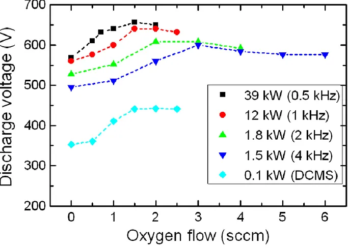
Fig. 1 shows the discharge voltage as a function of oxygen flow rates at different peak powers for HiPIMS and for DCMS. Introducing O2 in the chamber and increasing its flow rate drives the process from metal to compound mode through a transition region. The compound mode is reached and fully oxidized films are achieved when the voltages reach the maximum, as confirmed by optical characterization of grown films. It should be noted that only the increase in O2 flow was monitored in this work. The change in the discharge voltage with increasing O2 flow rates is related with changes of the secondary electron yield of the oxide covered surface [22]. In Fig. 1, it can be seen for HiPIMS that for higher peak powers the amount of flow which is required to reach compound mode is lower than for lower peak power.
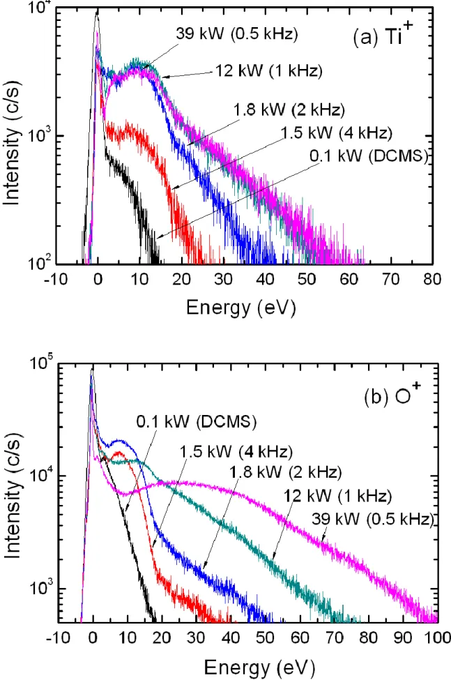
Ion energy distribution functions (IEDF) for Ti+ and O+ measured for each deposition condition are shown in Fig. 2. They all show a main peak at low energy and a shoulder extending to a high energy tail. The peak at lower energy in the respective IEDF corresponds to the thermalized ions [23]. The second peak (shoulder) and the high energy tail represent the energy distribution of the sputtered material at the target surface plus any acceleration that might occur in the plasma [24,25]. The HiPIMS conditions with the highest peak power (39 kW) show the highest ion energies. There is a prominent difference in the energy of the tail
between Ti+ and O+. The energy tails extend to higher values for O+ as compared to the Ti+ in all cases. The measured IEDF of Ar+ (not shown) does not show energies over a few eV similar to what is presented by Lattemann et al. [26].
Fig. 1. Discharge voltage versus O2 flow rates for the DCMS and HiPIMS at different peak powers.
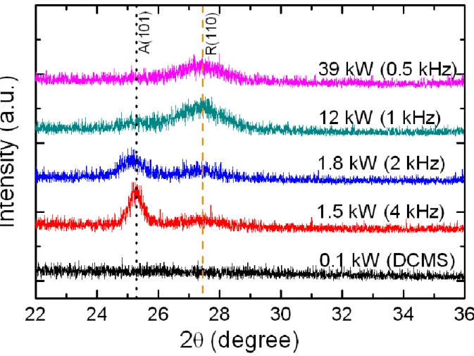
XRD-measurement was done for 2θ-values between 20 and 65°. In Fig. 3 the results for angles between 22 and 36 illustrate the obtained results with peaks from anatase (101) and rutile (110). The DCMS film shows no diffraction peak suggesting that the grown film is amorphous. The HiPIMS films show mixed phase composition with mainly rutile for high peak power (39 kW) and mainly anatase for low peak power (1.5 kW). This can be understood since the crystallinity and variation in the phase composition of TiO2 films depends on the energy of the arriving particles. At lower energy, given that it is sufficient to grow crystalline film, the deposited film shows anatase phase while at higher energy the rutile
Fig. 3. Grazing incidence X-ray diffractograms for the films grown with DCMS and HiPIMS.
phase is observed [12,13]. The energy input in the case of DCMS obviously does not provide sufficient energy to drive the structure from amorphous to crystalline, while for HiPIMS all films show a crystalline structure with more rutile the more energetic HiPIMS depositions are used. The observed dominant rutile phase at high peak power (39 kW) is therefore a consequence of more energetic arriving species. The major contribution in driving the structure of the film towards rutile is Ti+ and O+. However, the influence from O-, not measured in this work may also play an important role as shown in a recent study showing strong effect of energetic O- ions on the structure formation of TiO2 [27]. The energies of the negative ions depend on the discharge voltage which accelerates them towards the growing film surface. As shown in Fig. 1, the discharge voltage increases with an increase in peak
power. Thereby, increasing peak power also leads to increasing energy of the arriving O- ions. This is consistent with the study [27].
The trends of the refractive indices and the film density, as listed in Table 1, follow each other with the highest values for the film grown using 1.8 kW peak power (2 kHz) that consists of a mixed rutile and anatase phase. For more energetic bombardment (higher peak power) there is a decreasing trend in both values, while for DCMS and for the HiPIMS film with the lowest peak power (1.5 kW, 4 kHz) the density and refractive indices are significantly lower. The latter is understandable since amorphous and anatase phases have lower intrinsic density and refractive indices. However, the maximum of the density and refractive index for the film grown at 1.8 kW, which contains a mixture of the anatase and rutile phases, is an interesting result which requires further investigation. It can be speculated that a very high energy of the bombarding ions may cause lattice defects and thereby decreasing the density. This in turn means that an optimum energetic (moderate energy) bombardment is required for obtaining the optimum film density and refractive index. Similar behavior was observed by Amor et al. [28] for TiO2 films annealed at different temperatures.
4. Conclusion
We have obtained dense anatase and rutile phases of TiO2 films with reactive HiPIMS at room temperature, without using a substrate bias and any post-deposition annealing. The ratio between these phases depends on the peak power in the HiPIMS discharge. Using high peak power the rutile phase is observed while for lower peak power mainly anatase is detected. The ion energy distribution functions show that O ions in the plasma are more energetic than the Ti ions. The highest refractive index and density of the grown films are obtained at intermediate peak power where the film contains a mixture of the anatase and rutile phases and the deposition rate is relatively high.
Acknowledgements
This work has been supported by the Swedish Research Council (contract 621-2008-3222) and the Swedish Foundation for Strategic Research through the Strategic Research Center in Materials Science for Nanoscale Surface Engineering (MS2E). One of the authors (M. Aiempanakit) would like to thank the Ministry of Science and Technology, Thailand for funding the studentship. We would also like to acknowledge the staff at the Tandem Laboratory, Uppsala University, for technical assistance as well asKnut and Alice Wallenberg foundation.
References
[1] S. Berg, T. Nyberg, Thin Solid Films 47 (2005) 215.
[2] D. Rosen, I. Katardjlev, S. Berg, W. Moller, Nuclear Instruments & Methods in Physics Research Section B-Beam Interactions with Materials and Atoms 228 (2005) 193. [3] W. D. Sproul, D. J. Christie, D.C. Carter, Thin Solid Films 491 (2005) 1.
[4] E. Wallin, U. Helmersson, Thin Solid Films 516 (2008) 6398.
[5] K. Sarakinos, J. Alami, C. Klever, M. Wuttig, Surface & Coatings Technology 202 (2008) 5033.
[6] U. Helmersson, M. Lattemann, J. Bohlmark, A.P. Ehiasarian, J.T. Gudmundsson, Thin Solid Films 513 (2006) 1.
[7] V. Kouznetsov, K. Macak, J.M. Schneider, U. Helmersson, I. Petrov, Surface & Coatings Technology 122 (1999) 290.
[8] K. Sarakinos, J. Alami, S. Konstantinidis, Surface & Coatings Technology 204 (2010) 1661.
[9] M. Aiempanakit, P. Larsson, K. Sarakinos, J. Jensen, T. Kubart, U. Helmersson, Submitted to Thin Solid Films (2010).
[10] M. Audronis, V. Bellido-Gonzalez, Thin Solid Films, 518 (2010) 1962.
[11] T. Kubart, M. Aiempanakit, J. Andersson, T. Nyberg, S. Berg, U. Helmersson, Surface & Coatings Technology, in press, doi:10.1016/j.surfcoat.2011.01.019.
[12] V. Stranak, M. Quaas, H. Wulff, Z. Hubicka, S. Wrehde, M. Tichy, R. Hippler, Journal of Physics D-Applied Physics 41 (2008) 055202.
[13] J. Alami, K. Sarakinos, F. Uslu, C. Klever, J. Dukwen, M. Wuttig, Journal of Physics D: Applied Physics (2009) 115204.
[14] S. Konstantinidis, J.P. Dauchot, A. Hecq, Thin Solid Films 515 (2006) 1182. [15] K. Sarakinos, J. Alami, M. Wuttig, Journal of Physics D-Applied Physics 40 (2007) 2108.
[16] C.M. Herzinger, B. Johs, W.A. McGahan, J.A. Woollam, W. Paulson, Journal of Applied Physics 83 (1998) 3323.
[17] Z.C. Wang, U. Helmersson, P.O. Kall, Thin Solid Films 405 (2002) 50.
[18] W.M. Haynes, CRC Handbook of Chemistry and Physics, CRC Press/Taylor and Francis, Boca Raton, FL, 2010.
[19] D. Mergel, Thin Solid Films 397 (2001) 216. [20] S.Y. Kim, Applied Optics 35 (1996) 6703.
[22] D. Depla, S. Heirwegh, S. Mahieu, J. Haemers, R. De Gryse, Journal of Applied Physics 101 (2007) 013301.
[23] J. Bohlmark, M. Lattemann, J.T. Gudmundsson, A.P. Ehiasarian, Y.A. Gonzalvo, N. Brenning, U. Helmersson, Thin Solid Films 515 (2006) 1522.
[24] S. Kadlec, C. Quaeyhaegens, G. Knuyt, L.M. Stals, Surface & Coatings Technology 89 (1997) 177.
[25] D. Lundin, P. Larsson, E. Wallin, M. Lattemann, N. Brenning, U. Helmersson, Plasma Sources Sci. Technol. 17 (2008) 035021.
[26] M. Lattemann, U. Helmersson, J. E. Greene,Thin Solid Films, 518 (2010) 5978. [27] A. Amin, D. Kohl, M. Wuttig, Journal of Physics D-Applied Physics 43 (2010) 405303.
[28] S.B. Amor, G. Baud, J.P. Besse, M. Jacquet, Materials Science and Engineering B-Solid State Materials for Advanced Technology 47 (1997) 110.
Table 1
Deposition conditions used for sample preparation and summary of the film properties. Inserted are reference values for the two TiO2-phases.
Deposition mode Repetition frequency [kHz] Power (maximuma) [kW] O2 gas flow [sccm] Mass-deposition rate [μg/cm2 min] Deposition rate [nm/min] Film density [g/cm3] Refractive index (at 550 nm) Estimated errorsb 6 % 3 % 9 % 0.02% HiPIMS 0.5 39 1.5 2.1 5.4 3.9 2.60 HiPIMS 1.0 12 1.5 2.6 6.2 4.2 2.62 HiPIMS 2.0 1.8 2.5 4.0 9.4 4.3 2.63 HiPIMS 4.0 1.5 3.2 4.0 9.9 4.0 2.48 DCMS n.a. 0.10 1.5 3.8 10.2 3.8 2.36 Reference values Density [g/cm3] Refractive indexc (at 550 nm) Anatase 3.84 [18,19] 2.57 [19,20] Rutile 4.23 [18,19] 2.75 [18,19] a
For HiPIMS this is the peak power, while for DCMS it is the actual power level used. b
Estimated absolute errors. Relative errors are considerably smaller, less than half, making analysis of trends meaningful. For the refractive index, the error is based on the 90% confidence limits for fitted parameters [16].
c
The averaged refractive index values were calculated by using data from Ref. [19] and they correspond to the values read from Fig. 3 in Ref. [20].