In
A
Vo
nstitu
D
A Stud
ltage-C
Maste
Departme Linköpin S-581 83ution
Departm
dy and
Contro
er thesis
L LI ent of Electr g University Linköping,nen f
ment of E
Exam
Desig
olled O
Tech
perform
Kamra
LiTH-ISY-Dece TEKNISK INKÖPING ical Enginee y Swedenför s
Electrica
mensarbe
n of H
Oscillat
hnolog
med in El
by
an Afgh
-EX--12/46 ember 201 KA HÖGSK GS UNIVE ering L I 5syste
al Engine
ete
igh Pe
tors in
gy
lectroni
hari
646--SE 2 KOLAN ERSITET Linköpings t Institutionen 581 83 Linköemte
eering
erforma
65nm
ic Devic
tekniska hög n för systemt öpingknik
ance
CMOS
ces
gskola teknikk
S
A Study and Design of High Performance
Voltage-Controlled Oscillators in 65nm CMOS
Technology
Master thesis
Performed in Electronic Devices
Department of Electrical Engineering
Linköping Institute of Technology
by
Kamran Afghari
LiTH‐ISY‐EX‐‐12/4646‐‐SE
Supervisor
:
Assoc. Professor Jerzy Dabrowski
Fahad Qazi
Linköping University
Examiner: Assoc. Professor Jerzy Dabrowski
Linköping University
Linköping, December 2012
Presentation Date 2012-12-17
Publishing Date (Electronic version)
Department and Division
Department of Electrical Engineering
URL, Electronic Version http://www.ep.liu.se
Publication Title
A Study and Design of High Performance Voltage-Controlled Oscillators in 65nm CMOS Technology Author(s)
Kamran Afghari
Abstract
In recent years, oscillators are considered as inevitable blocks in many electronic systems. They are commonly used in digital circuits to provide clocking and in analog/RF circuits of communication transceivers to support frequency conversion. Nowadays, CMOS technology is the most applicable solution for VLSI and especially for modern integrated circuits used in wireless communications. The main purpose of this project is to design a high performance voltage-controlled oscillator (LC VCO) using 65nm CMOS technology. To meet the state-of-the-art requirements, several circuit solutions have been explored and the design work ended-up with a Quadrature VCO. The circuit operates at center frequency of 2.4 GHz. The phase noise of QVCO obtained by simulation is -140 dBc/Hz at 1MHz offset frequency which is 6 dB less compared to conventional LC VCOs. The power consumption is 3.6mW and the tuning voltage can be swept from 0.2 V to 1.2 V resulting in 2.25 GHz - 2.55 GHz frequency range.
Keywords
QVCO, Power Consumption, Phase Noise, Tuning Voltage, Communication Transceivers Language
English
Other (specify below)
Number of Pages 74 Type of Publication Licentiate thesis Degree thesis Thesis C-level Thesis D-level Report
Other (specify below)
ISBN (Licentiate thesis)
ISRN: LiTH-ISY-EX--12/4646--SE Title of series (Licentiate thesis)
Series number/ISSN (Licentiate thesis)
Abstract
In recent years, oscillators are considered as inevitable blocks in many electronic systems. They are commonly used in digital circuits to provide clocking and in analog/RF circuits of communication transceivers to support frequency conversion. Nowadays, CMOS technology is the most applicable solution for VLSI and especially for modern integrated circuits used in wireless communications. Additionally, the trend towards single chip implementation makes the circuit design increasingly challenging.
The main purpose of this project is to design a high performance voltage‐ controlled oscillator (LC VCO) using 65nm CMOS technology. In the beginning, a brief study of different VCO architectures is carried out. Next, a wide comparison between different VCO topologies is performed in terms of phase noise and power consumption. The effect of VCO phase noise on RF transceivers is also analyzed. In the following, all the phase noise contributors in a typical LC VCO are identified to enable design optimization.
To meet the state‐of‐the‐art requirements, several circuit solutions have been explored and the design work ended‐up with a Quadrature VCO. The design is verified for the intended tuning range and process, temperature, and supply voltage (PTV) variations.
The circuit operates at center frequency of 2.4 GHz. The phase noise of QVCO obtained by simulation is ‐140 dBc/Hz at 1MHz offset frequency which is 6 dB less compared to conventional LC VCOs. The power consumption is 3.6mW and the tuning voltage can be swept from 0.2 V to 1.2 V resulting in 2.25 GHz ‐ 2.55 GHz frequency range.
Acknowledgments
First, I should show my gratitude to Professor Jerzy Dabrowski for his support and supervision during the project. He showed patience for solving problems encountered throughout my thesis. The smart suggestions provided by Professor Jerzy Dabrowski gave me a new inspiration for designing a state of the art circuit. Furthermore, his experience and knowledge helped me to tackle the problems quicker.
I should appreciate the PhD students in Electronic Devices for giving me some advice during my thesis. Also, I am really grateful to all of my friends for sharing happy moments in Linköping University.
Here, I would like to thank my parents for supporting me during my studies. They always encouraged me to do my best during the stressful moments in my life. Last but not least, I should thank my brother, Erfan, for his support and persuasion during my project.
Contents
Abstract………... vii Acknowledgments………... ix Abbreviations……….. xix 1. INTRODUCTION………... 1 1.1 Objective and Scope……….. 1 1.2 VCO Design Specifications………. 2 1.3 VCOs in Phase‐Locked Loops……….. 3 1.4 Thesis Organization……….. 3 2. OSCILLATOR BASICS……… 5 2.1 Introduction……….. 5 2.2 Oscillator Transfer Function……….. 5 2.3 Ring Oscillators……….. 7 2.4 LC Oscillators………... 10 2.4.1 LC Tank………. 10 2.4.2 One‐port Model of LC VCO……… 12 2.4.3 Cross‐Coupled LC Oscillator……….…. 13 2.4.3.1 NMOS Cross‐Coupled LC Oscillator……… 14 2.4.3.2 CMOS Cross‐Coupled LC Oscillator……….…… 173. OSCILLATOR NOISE……….. 20 3.1 General Idea……….. 20 3.2 Phase Noise Effect on RF Transceiver Topologies……… 22 3.3 Analysis of Oscillator Phase Noise……….. 24 3.3.1 Leeson’s Equation of Phase Noise………. 24 3.3.2 Hajimiri and Lee’s Phase Noise Equation………. 29 3.3.3 F‐Parameter………. 35 3.4 Analysis of Phase Noise Sources in CMOS LC VCOs……… 36 3.4.1 Transistor Noise Contribution………. 36 3.4.2 Noise Contributors in MOSFET……… 37 3.4.2.1 Thermal Noise……… 37 3.4.2.2 Flicker Noise……… 39 3.4.2.3 Bias Noise………. 39 3.4.2.4 Switching Pair Noise……… 40 3.4.2.5 Resonator Noise………... 40
4. STATE‐OF‐THE‐ART DESIGN………. 41 4.1 Introduction……… 41 4.2 Low Phase Noise QVCO……….. 41 4.2.1 Circuit Design……… 42 4.2.2 Design Specifications……….. 44 4.2.3 Simulation Results………. 45 4.3 Low Noise Low Power CMOS LC VCO……….. 45 4.3.1 CMOS LC VCO………. 46 4.3.2 Power Analysis……….. 48 5. LC VCO DESIGN……… 52 5.1 CMOS Cross‐Coupled Models……….……. 52 5.1.1 Analysis and Comparison……….…. 52 5.1.2 Design Procedure………..…. 57 5.1.2.1 Cross‐Coupled LC VCO……… 57 5.1.2.2 NMOS LC VCO……….……. 60 5.1.2.3 PMOS LC VCO……….…. 62 5.1.3 Comparison of Different VCO Topologies……….…. 63 5.2 Bias Circuitry Design……….. 65
6. COMPLEMENTARY SIMULATIONS AND RESULTS………..….…… 66 6.1 Introduction……….… 66 6.2 Phase Noise and Frequency vs. Control Voltage……….… 66 6.3 Reference Current Source Variation……… 67 6.4 Phase Noise and Frequency vs. Temperature……….………. 68 7. CONCLUSION………. 70 7.1 Summary……….………... 70 7.2 State‐of‐the‐Art Comparison………... 71 References……….…… 72
List of Figures
Figure 2.1: Oscillator’s feedback system……….…… 6 Figure 2.2: Ring oscillator architecture………... 7 Figure 2.3: Current starved inverter………..… 8 Figure 2.4: Differential symmetric pair……….… 9 Figure 2.5: Series resistance conversion into equivalent parallel resistance……… 11 Figure 2.6: Phase behavior and magnitude of a resonator………...12 Figure 2.7: One‐port model of an LC VCO……….……... 13 Figure 2.8: Bottom biased LC oscillator with equivalent losses………14 Figure 2.9: NMOS LC oscillator analysis………..……… 15 Figure 2.10: Waveforms of a cross‐coupled LC oscillator……… 16 Figure 2.11: Top‐biased complementary LC oscillator……….. 18 Figure 3.1: Comparison of phase and jitter noise………. 21 Figure 3.2: Output waveforms comparison of an ideal and a real oscillator………. 22 Figure 3.3: Phase noise impact on receivers……… 23 Figure 3.4: Phase noise impact on transmitters……… 24 Figure 3.5: LC oscillator model with noise generators………. 25 Figure 3.6: Phase noise spectrum of a real oscillator……… 28 Figure 3.7: Impulse response of an ideal oscillator……… 29 Figure 3.8: Impulse impact on a time‐varying system………. 30 Figure 3.9: Amplitude noise of an oscillator in one period………..……….. 30Figure 3.10: Current impulse behavior on a time‐varying system………... 30 Figure 3.11: Impulse sensitivity function of a real oscillator……….…… 31 Figure 3.12: Current impulse effect on the output signal……….…..32 Figure 3.13: ISF block diagram………..…….33 Figure 3.14: Procedure of current noise conversion into phase noise………….……..34 Figure 3.15: Noise sources in LC cross‐coupled VCO……….……….36 Figure 3.16: Lumped noise model……….37 Figure 4.1: Circuit schematic of Quadrature VCO……….…….42 Figure 4.2: Conventional Quadrature VCO………..…. 43 Figure 4.3: CMOS LC oscillator circuit schematic……….…. 47 Figure 5.1: Different designs of CMOS cross‐coupled VCO……….….. 53 Figure 5.2: NMOS phase noise at 100 kHz offset frequency……….… 54 Figure 5.3: PMOS phase noise at 100 kHz offset frequency………..55 Figure 5.4: CMOS phase noise at 100 kHz offset frequency……….……….55 Figure 5.5: NMOS phase noise at 1MHz offset frequency………..56 Figure 5.6: PMOS phase noise at 1MHz offset frequency……….…. 56 Figure 5.7: CMOS phase noise at 1MHz offset frequency……….…. 57 Figure 5.8: CMOS cross‐coupled LC oscillator with NMOS bias circuit……….. 58 Figure 5.9: Phase noise of CMOS cross‐coupled VCO with NMOS bias circuit……. 59 Figure 5.10: Phase noise of CMOS cross‐coupled VCO with PMOS bias circuit... 60 Figure 5.11: Phase noise of self‐biased CMOS cross‐coupled VCO……….. 60
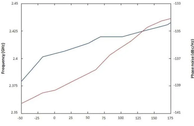
Figure 5.13: Phase noise of NMOS VCO with PMOS bias circuit……… 61 Figure 5.14: Phase noise of PMOS VCO with NMOS bias circuit……… 62 Figure 5.15: Phase noise of PMOS VCO with PMOS bias circuit………. 63 Figure 6.1: QVCO phase noise (red) and frequency (blue) versus control voltage……… 67 Figure 6.2: Impact of reference current source variation on QVCO center frequency………. 68 Figure 6.3: Impact of temperature variation on QVCO phase noise (red) and frequency (blue)……….. 69
List of Tables
Table 1.1: Ultimate VCO design specifications……….. 2 Table 5.1: CMOS cross‐coupled LC VCO dimensions……….. 58 Table 5.2: NMOS cross‐coupled LC VCO dimensions…...61 Table 5.3: PMOS cross‐coupled LC VCO dimensions………62 Table 5.4: Comparison of different VCO topologies regarding the phase noise and power consumption……….. 64 Table 7.1: State‐of‐the‐art comparison... 71Abbreviations
VCO Voltage‐Controlled Oscillator QVCO Quadrature Voltage‐Controlled Oscillator Q Quality factor FOM Figure of Merit PLL Phase‐Locked Loop MOSFET Metal Oxide Semiconductor Field Effect Transistor IF Intermediate Frequency RF Radio Frequency OFDM Orthogonal Frequency‐Division Multiplexing QAM Quadrature Amplitude Modulation DC Direct Current ISF Impulse Sensitivity Function AM Amplitude Modulation1. INTRODUCTION
Nowadays, oscillators are considered as inevitable blocks in many electronic devices. They are mainly applicable in communication systems such as radio transceivers. Also, other applications take advantage of high performance oscillators. For instance, clock generation in microprocessors can be achieved by some types of VCOs. Today, CMOS technology is the most popular solution for designing a high performance voltage‐controlled oscillator. It should be pointed out that in most cases a VCO is not a standalone block but rather a part of a larger system like PLL‐based frequency synthesizer.
1.1 Objective and Scope
The first objective of this project was a broad analysis of different VCO topologies used in the contemporary applications. A specific objective was to design a high performance VCO based on a design study of different LC VCO circuits. By practical comparison of critical specifications like phase noise and power consumption the choice of the right circuit could be done. To meet the state‐of‐ the‐art specifications, a quadrature VCO (QVCO) was chosen as the ultimate design goal.The QVCO was assumed to drive a balanced mixer for frequency conversion in a data OFDM transceiver. Since the OFDM‐QAM signal is extremely sensitive to the local oscillator phase noise, the phase noise was the primary specification that the QVCO was optimized for. Additionally, to check for the application in a PLL, the process, temperature, and supply voltage (PTV) variations and tuning range were taken carefully into account.
1.2 VCO Design Specifications
To design a VCO, different requirements should be fulfilled. In this section, we define the VCO metrics individually. In particular, we should meet the oscillation frequency, power consumption, tuning range and phase noise requirements which are the most important in a VCO design. The oscillation frequency may vary from one design to another due to different applications and architectures. The tuning voltage range is determined by required frequency variations in different applications. The other major issues that should be considered especially in a high performance VCO design are phase noise and power consumption. Generally, it is difficult to fulfill all of the requirements at the same time. For instance, there is usually a tradeoff between power consumption and phase noise. On the other hand, some VCO topologies can improve the phase noise performance while other architectures can dissipate less power. Consequently, regarding the design specifications and their priorities, the designers have to choose the appropriate VCO topology but still are exposed to design tradeoffs. The specifications for our ultimate VCO design aimed at 65‐nm CMOS technology are as shown in Table 1.1.
QVCO specifications Value Center frequency 2.4 GHz Supply voltage 1.2 V Phase noise at 1MHz offset frequency < ‐130 dBc/Hz Power consumption < 5 mW Tuning voltage 0.2 ‐ 1.2 V Frequency range 2.25 ‐ 2.55 GHz Table 1.1: Ultimate VCO design specifications
1.3 VCOs in Phase‐Locked Loops
Voltage‐controlled oscillators are mostly implemented as a component of phase‐ locked loops (PLLs). PLLs can be used in different areas such as clocking of microprocessors, providing carriers for wireless transceivers or other transmission systems. Usually, in communication applications PLLs require VCOs with a wide tuning range to serve up‐ or down‐conversion over the system bandwidth. Interestingly, in PLLs the VCO phase noise requirements can be relaxed. In other words, the noise produced by a voltage‐controlled oscillator at the oscillation frequency will be to some extent filtered out by the system. Therefore, VCO topologies with wide tuning range are usually preferred.
In high performance applications where a low phase noise or jitter is required, VCOs using LC tanks are preferred for their high Q‐factor. Therefore, LC‐based VCOs will be in focus of the presented designs.
1.4 Thesis Organization
In this project, firstly, various VCO architectures are analyzed in detail. In particular, regarding phase noise and power consumption, a wide comparison is carried out. As a result, we have come up to the state‐of‐the‐art design in which the VCO specifications can be fulfilled.
In the following chapter, the foundations of the oscillator theory are discussed. Moreover, different VCO architectures such as the ring oscillator, negative gm oscillator, and CMOS LC VCOs are analyzed. At the end of this chapter the advantages and drawbacks regarding different topologies are compared.
In Chapter 3, we study the oscillator noise using different models acknowledged in literature. Afterwards, the phase noise is defined and its effect on an RF transceiver is analyzed. Finally, the phase noise contributors in a VCO are discussed.
In chapter 4, some state of the art topologies are presented and their specification requirements are defined.
In Chapter 5, seven variants of low‐noise low‐power LC VCO are designed for the same power consumption and then they are compared in terms of phase noise. In Chapter 6, complementary simulations of the QVCO regarding PTV variations are presented showing it is in line with the state‐of‐the‐art designs.
In Chapter 7, conclusions from the presented design are provided. At the end of this chapter, the performance of the designed LC QVCO circuit is compared with other reported LC VCOs.
2. OSCILLATOR BASICS
2.1 Introduction
In the second chapter, we describe the basic oscillation theory. This theory refers to the feedback system model or the negative resistance one‐port model. Different types of oscillators including the ring, negative gm oscillators, CMOS LC VCOs and some other topologies are discussed. Nowadays, among different types of oscillators, mostly the LC cross‐coupled VCOs are preferred. Hence, their advantages and drawbacks are mainly emphasized in this project.
2.2 Oscillator Transfer Function
A VCO can be modeled as a feedback system as shown in Fig. 2.1. The equivalent transfer function of this system can be formulated as:
G jω
HY HH(2.1)
According to the above equation, at the desired frequency of ω0, if H(jω0)=1, the closed loop gain will be driven to infinity. It causes the system noise to increase and produces a periodic signal. From another point of view, the oscillation will be stable if H(jω0) is precisely on the imaginary axis [11]. Practically, the small signal loop gain should be at least two to fulfill the initial oscillation conditions. As we know, this value decreases gradually and goes to unity as the amplitude improves due to the nonlinearities.
The following equations are two conditions that should be satisfied for the oscillation startup at ω0:
|H (jω
0)| = 1 , arg (H (jω
0)) = 0⁰
(2.2)
The pha negativ situatio complet sufficien grounde Nowada mention preferre ase in (2.2) e. These e ns, the tw tely. In o nt. For exa ed, even th ays, design ned in the ed in high f ) should be quations a wo above ther word ample, in s hough the Figure ners use v e above se frequency e changed are known e conditio ds, the Ba some prac startup co e 2.1: Osci various top ection. Mo oscillator to a value as Barkha ns can no arkhausen’ ctical cases onditions a llator’s fee pologies to oreover, L design. of 180⁰ w usen’s crit ot satisfy ’s criteria s, the outp are satisfied edback sys o satisfy th LC and rin when the lo teria. Howe the oscil are nece put remain d. tem he Barkha ng oscillato oopback ga ever, in sp llation sta essary but ns saturate ausen’s crit ors are ma ain is ecial artup not ed or teria ainly
2.3 Rin
A ring o a feedb output inverter followinf
N Conside stages i the diffeng Oscilla
oscillator is back loop. I of last in r cell det ng: N ering the p s chosen. erential antors
s a device c In other w verter is f termines ower cons There are nd the sing Figure composed words, the N fed back i the oscill sumption a different gle‐ended m e 1.2: Ring a) Dif b) Sing of an odd NOT gates into the f ation freq and phase topologies models are g oscillator fferential m gle‐ended d number o s are place irst one. T quency w noise perf s regarding e mainly di architectu model model of inverter d in a chai The total which is f formance, g the ring iscussed in ure s connecte in in which delay of e formulated ( the numbe oscillators n this proje ed in h the each d as (2.3) er of s but ect.
In sing Barkhau phase s cells. Th The int generat In orde apply a Anothe Fig. 2.3, the cell
le‐ended usen’s crit shift of 180 he current trinsic cap ted by the r to have a higher cur r improved , the frequ . model, as eria is alw 0⁰, the sin is only use pacitors ar transistors a quicker t rrent. d type of d uency can Figu s far as t ways satisfi ngle‐ended ed during t re charged s. Therefor transitions delay cell be control re 2.2: Cur the invert ied. Since d model is transitions d and disc re, the dela and highe is current‐ led when rrent starv ters have each dela designed of the NO charged b ay time of er oscillatio ‐starved in two extra ved inverte high out ay cell has with an o OT gates.
y this con each cell i on frequen nverter. As transistor er tput gain, a large si odd numbe nstant cur is defined. ncy, we sh s shown in s are adde the ignal er of rrent ould n the ed to
As show differen charge for a f improve NMOS t For a gi ring osc other w times h ended Additio the inv differen commo compon wn in the F ntial transi stored in t ixed frequ e the osci transistors ven powe cillator ha words, the igher than architect nally, it ha erse propo ntial ring os on noise r nents on t Fig. 2.4, th istors and the circuit uency. If P llator to b can be ap Figure r consump as a worse e different n the single
ure cons as a bette ortionality scillators a rejection [ he chip. N he differen an output and the cu PMOS tran be tunable pplied as cr e 2.3: Diffe ption, frequ e perform tial ring os e‐ended st umes les r phase no y of the p are often p [20]. More Nowadays, tial structu t load. Th urrent driv nsistors ar with diffe ross‐couple erential sym
uency and ance than scillator’s tructure [2 ss power oise for sp hase noise preferred in eover, less this archit ure consist e cell dela ing the loa re applied erent rang ed or symm mmetric pa number o n its single phase no 20]. On the than th pecific pow e to powe n digital cir s noise is tecture is
ts of an N ay is deter ad. Resisto d as our l ge of volta metric mod air of stages, t e‐ended c ise is N(1 e other ha he differe wer consum er dissipat rcuits due s injected widely use MOS or PM rmined by ors can be u loads, we ages. PMO dels. the differe ounterpar +Vchar/(RL* nd, the sin ential mo mption du tion. Howe to their be to the o ed for stat MOS y the used can OS or ntial rt. In *Itail)) ngle‐ odel. ue to ever, etter other te of
the art designs. For instance, a quadratic signal is generated by differential architecture since even number of inverters should be maintained.
Passive devices are not used in ring oscillators. Regarding this issue, there are benefits and drawbacks which can be discussed. The main advantage of using active elements is easy integration on chip. Additionally, inductors occupy a considerable amount of area on chip. However, using an inductor with a capacitor on the chip makes a band pass filter that leads to better phase noise performance. Overall, ring oscillators show worse phase noise performance than the LC VCOs. The main usage of ring oscillators is for data transmission as clock recovery or clock propagation on the chip.
2.4 LC Oscillators
An LC oscillator consists of a resonator tank in which the inductor and the capacitor are connected in parallel. There are various LC VCO architectures but Colpitts and Negative gm oscillators are the most popular structures. In the following sections, these two models are widely compared regarding their benefits and drawbacks.
2.4.1 LC Tank
In VCO implementation, LC network is mainly in focus due to its filtering benefits. Since the LC tank consists of an inductor and a capacitor connected in parallel, it is also called a parallel resonator circuit. In an ideal condition, if a current impulse is applied to the LC tank, the energy transfers back and forth between the inductance and the capacitance. This leads the circuit to oscillate for an infinite period time. However, this occurs in an ideal case where both of the elements are lossless. In other words, some dissipation is inevitable for the inductor and the capacitor. Otherwise, they should have an infinite quality factor that is not possible in practice. Actually, the resonator’s loss is due to the series resistances of the inductor and the capacitor. As far as RF VCOs oscillate over a small range of
frequen The ove It dissip compen tank. Th it helps Figu The ma occupy oscillato The ma resonan purely r
f
Where, ncies, the p erall resista pates the e nsate this his active c the oscilla ure 2.4: Se in drawba a larger ors have a gnitude an nce freque real. The re √LCL and C ar parasitic re ance is sho energy and lossy circu circuit prod ation to sur eries resista ck is that area on t better pha nd phase b ency, the n esonance f
re inductan esistances own by Rp i d thus lea uit, an activ duces a neg rvive. ance conve integrated the chip t ase noise p behavior o network be frequency
nce and ca can be rem in the follo ds the osc ve circuit s gative resi ersion into
d inductors than the performan of an LC ta ehaves like is formula
pacitance modeled to owing figur cillation to should be stance to c o equivalen s have very ring oscill ce compar nk is show e a resistan ted as follo
respective o their par res.
o fade awa added in cancel the nt parallel y low qual lators. Ne red to ring wn in the F nce. In oth owing:
ely. rallel struct
ay. In orde parallel to Rp. Theref resistance ity factors vertheless g oscillators Fig. 2.6. At her words,
ture. er to o the fore, e s and s, LC s. t the , it is (2.4)
2.4.2 O
Negativ two ind much e As men and the prevent energy. compen with the satisfied GR
FigurOne‐port
ve gm or o ividual one asier. The ntioned be e capacitor ts oscillatio Therefore nsate the l e infinite p d by the foR
e 2.5: PhaModel of
ne‐port m e‐port mod procedure fore, the r can be m on to be s e, an activ oss of the parallel res ollowing eq ase behaviof LC VCO
model repr dels. This a e is depicte resonance modeled a stable by c ve negativ tank. In ot sistance at quation: or and mag esents the approach m ed in the Fi e circuit w s its paral consuming ve resistan ther word t the reson gnitude of e oscillato makes the ig. 2.7. ith the ser llel equiva g some am nce which s, we shou nance freq f a resonat r as the c analysis o ries loss o alent. At e mount of s is equal uld create quency. Th or ombinatio of LC oscillaof the indu ach period stored LC to –Rp sh a lossless his conditio ( on of ators uctor d, Rp tank ould tank on is (2.5)
As men VCO is i
2.4.3 C
As men neutrali VCO, th oscillati times l topolog LC osci coupled self‐bias tioned ear n stable coCross‐Cou
tioned in a ized by ac he transis on startup arger than gy is the sim llator is c d. Each of sing curren Figure rlier, Gm is ondition.upled LC O
above sect ctive devic stors act s p conditio n the par mple desig categorized them can nt source. 2.7: One‐p called asOscillator
tions, in ne es for a st similar to n, negativ rallel loss gn and imp d into thr be imple port model the large sr
egative Gm table oscil an active e resistan of the ta plementati ee types: mented us l of an LC V signal tran m procedur llation. In e negative ce usually ank. The m ion on the PMOS, N sing top‐b VCO nsconducta re, the loss CMOS cro e resistan y is definedmain adva e chip. The NMOS and biased, bot ance when s of the ta oss‐couple ce. To sa d at least antage of cross‐cou CMOS cr ttom‐biase n the nk is d LC atisfy two this pled ross‐ ed or
2.4.3.1
As show present differen losses a In this simplici mode n assump resistan differen and –Vo V I1 NMOS C
wn in the ted. The lo ntial pair a are analyze Figure section, ty, the cir noise is gr ption is not nce. As we nce of 180 out. The res V G VCross‐Cou
Fig. 2.8, a osses of th and two r ed in detail 2.6: Bottom the NMO rcuit is div rounded so t complete e know, th 0⁰. Therefo sistance se Gupled LC O
a bottom‐ he tanks a esonators l. m biased L OS cross‐co ided into o that the ely true be he output ore, the ga en from ouOscillato
biased NM re depicte in which LC oscillato oupled LC two parts. e Vsource is ecause the nodes hav ates of the utput noder
MOS cross‐ ed as well.
their seri
or with equ
C oscillato . It is assu biased to current so ve differen e transisto e to groun ‐coupled L It consist es and pa uivalent los
or is analy umed that o ground.
ource has ntial swing ors are exp d is formu LC oscillato ts of an NM arallel resis sses yzed. For the comm However, a finite ou g with a p pressed as lated as: or is MOS stive the mon‐ this utput hase Vout (2.6)
Therefo in which For a c should in the m In the a two. Next, w large si gain. As will dec nonline transist output transco region. transco ore, if the t h: Lp=2Lp1 , cross‐coup be greater minimum c
α
R
bove equa we should f gnal gain. s the oscill crease. Fin arities. Th ors functio swing is nductance Actually, nductance Figure two tanks a , Cp=Cp1/2, led VCO t r than unit ase. There ation, αmin find out th The smal ation ente nally, it w he nonlin on in triodclipped un e of an N
in linear e to drain v
e 2.7: NMO
are same, Rp=2Rp1 a to be in s
ty. Therefo efore, the s satisfies th he relation l signal ga ers the ste
ill be equ ear chara de and cu nder the MOS tran region, w voltage. On OS LC oscill we can co and the neg table cond ore, the ga startup con he startup nship betw ain is αmin
ady state, al to the acteristic i ut‐off regio bias volta sistor is e we have t n the othe lator analy nvert them gative resi dition, the ain value s ndition is a condition ween the s times larg the small large sign is figured on. In cut‐ age. Additi equal to µ the direct r hand, by ysis m to an equ istance wo e small sig should be as followin which sho small signa ger than th signal gain nal gain b out by ‐off region ionally, th µnCox (W/L t proportio y applying a uivalent ci ould be ‐2/ gnal loop chosen as g: ( ould be at l al gain and he large si n of the ci ecause of analyzing n, the pos he large si L) Vds in li onality of a small vol rcuit Gm1. gain two (2.7) least d the ignal rcuit f the the sitive ignal near the tage
of ∆V at enough and the As obse Therefo depicte output obtaine current
V
t Vg1, the V , the trans e loop gain erved in th ore, each td as a squ would be ed at the c harmonic
I
R
Figu Vg2 or Vd1 w sistor will e will be sta he results, transistor uare wave the same enter freq s so the ou ure 2.8: Wa will decrea enter the li able at one symmetr is on in ha form for eas for the quency is e utput amp aveforms o ase corresp inear regio e. ical wavef alf of the each trans e circuit o equal to (1 litude is fo of a cross‐c pondingly. on. Here, th forms are period so sistor [21]. perating in 1/π)Ibias. Th ormulated coupled LC If ∆V is co he gm1 star obtained the curre The mea n DC mod he LC tank as: C oscillator onsidered l rts to decr
at the out ent behavi
n value of e. The cur filters out ( r arge ease tput. or is f the rrent t the (2.8)
2.4.3.2 CMOS Cross‐Coupled LC Oscillator
A CMOS cross‐coupled LC oscillator consists of two NMOS and PMOS transistor pairs. In this topology, usually one inductor is used. A differential voltage is applied on the inductor which leads to better output waveforms than the previous topology. To obtain symmetrical waveforms, we should generate equal parallel resistance on the both sides of the resonator. If not, the phase noise would increase. Therefore, if the inductance is not designed symmetrical, two inductors in series should be implemented alternatively.
In this structure, as shown in Fig. 2.11, the PMOS transistors reuse the bias current. Therefore, a larger output voltage is generated. As the output voltage increases, one of the NMOS transistors is switched on while the other one goes off. This is the same case for the PMOS pair but in the other way. For instance, in the half period, the current is driven into the M4 and then the resonator and finally it is conducted by the M1. One of the advantages of this structure over other topologies is that the current goes through the resonator’s resistance in each half period. Consequently, the output would be twice larger than the PMOS or NMOS cross‐coupled architecture. Regarding the Leeson’s equation, the output voltage improvement leads to better phase noise performance.
Additionally, the PMOS transistors produce an extra negative resistance which can increase the overall negative resistance when added to NMOS pair. Consequently, the complementary architecture obtains an overall negative resistance of ‐2/Gm,NMOS‐2/Gm,PMOS. To produce symmetrical waveforms, the NMOS and PMOS transconductance should be the same. So, the overall negative resistance would be ‐4/Gm. Additionally, when using the complementary architecture, the startup condition would be satisfied easily for a specific bias current.
Moreover, when equal transconductance is considered for the NMOS and PMOS pair, the most symmetric output can be obtained comparing to the NMOS or PMOS cross‐coupled counterparts. Therefore, the rise and fall times will boost and hence the flicker noise upconversion will improve [20]. In our design, we
obtain a coupled PMOS t There a encoun coupled swing is degrade be more In a co extra pa PMOS a PMOS t the ov a more re d architect ransistors are also so ter some o d architect s set at Vdd es to (Vdd‐V e influence Fig mplement arasitic cap and NMOS transistors verall tra asonable ture. The are the m ome draw output sw ture, cons d‐Vdiff while Vdiff)/2. Ho ed by the s gure 2.9: T tary LC arc pacitances S sizing ma should be ansconduct phase nois 1/f2 phase ain contrib backs whe ing constra sidering th e in a com owever, wh supply volt Top‐biased chitecture seen in th ay vary co e chosen qu tance of se in 1/f3 e noise is butors of th en using C aints in th he voltage mplementa hen the ou tage distor complem , adding P he resonat rrespondin uite larger the de region com improved hermal no CMOS cros is architec e headroo ry architec utput is bia rtions. entary LC PMOS pair or. Regard ngly. In ot r than NMO esign. The mpared to d as well. ise in this ss‐coupled cture. In an om, the o cture the o ased at Vdd oscillator r to the c ding the bia ther words OS pair. Th erefore, o NMOS cr However, region. LC VCOs. n NMOS cr output vol output vol d, the VCO ircuit lead as current, s, the sizin his will bala the requ ross‐ the We ross‐ tage tage O will ds to , the ng of ance uired
transconductance is met in the complementary LC architecture. Since the overall intrinsic parasitic capacitance enhances in this topology, the resonator value should be calculated carefully to meet the desired oscillation frequency. Consequently, decreasing the value of the capacitor leads to tuning range limitations.
3. OSCILLATOR NOISE
In this chapter, we mainly describe the oscillator phase noise. In the beginning, a brief definition of the phase noise is given. Afterwards, its effect on RF transceivers is analyzed. In the following sections, the Leeson’s phase noise model is discussed and followed by two other models using the impulse sensitivity function. Finally, a detailed analysis of the phase noise sources in a complementary LC oscillator is carried out.
3.1 General Idea
There are some types of noise sources which influence the functionality of an LC VCO. The external noise is produced by the other components that are interacting with the oscillator. The filter generating the tuning voltage of the oscillator and the frequency divider in a Phase‐Locked Loop are the blocks which can produce extrinsic noise in our circuit. The internal noise is generated by the circuit layout of the components designed in the VCO. As a matter of fact, both noise sources can inject some disturbances into our design. Therefore, the output amplitude and frequency are influenced by this issue. Since the transistors nonlinearities compensate the amplitude noise, its effect is commonly neglected during the VCO design. Actually, a small deviation of frequency is regarded as phase noise in analog circuits. Nevertheless, if we consider the output in a time‐dependent scale, it is considered as a deviation in zero crossing points. The phase noise plays an important role in VCO functionality. In the digital circuits, phase noise can be defined as jitter. In the Fig. 3.1, the difference can be identified clearly.
We can wavefo frequen output
x(t)= A
For smasin(φ
n(
cos(φ
n Therefox(t) ≈ A
As show compar signals undesir oscillato noise is F n formulat rm is sinus ncy and φn signal canA[cos(ω
0t
all values o(t)) ≈ φ
n(t
(t)) ≈ cos
ore, the ouAcos(ω
0t)
wn in the F red. Moreo to some ed signals or spectrum similar to Figure 3.1:te the circ soidal whe (t) is the c be rewritt
)cos(φ
n(t
of phase not)
(0) = 1
tput is app− Aφ
n(t)s
Fig. 3.2, th over, the r extent. A are obser m differs f a skirt in f Comparis uit output ere A is the correspond ten as follo))−sin(ω
0 oise, we ge proximatedsin(ω
0t)
he output w resonator As we mo rved due to from what frequency on of phas t as x (t) = e amplitud ding phase owing:t)sin(φ
n(t
et: d as follow waveform is respons ove away o the filter is expecte domain. se and jitte = Acos [ω de of VCO, e noise. Fot))]
wing: of an idea sible for w from the ring techni ed in theor er noise ω0t + φn (t ω0 is the or a detaile al and a re wiping out center fr ique. Ther ry. In pract )]. The ou desired ce ed analysis, ( ( ( ( eal oscillat the unwa requency, refore, the tice, the p utput enter , the (3.1) (3.2) (3.3) (3.4) tor is nted less real haseFig Here, w Therefo distance (3.5). T logarith corresp
L ∆ω
Ptone sho a 1Hz b dBc/Hz much th3.2 Pha
As we k This fre should near ou unwant and the gure 3.2: O we propose ore, we shoe is called o obtain t hmic scale onding for
10 log
ows the no bandwidth which rep he Ptone is base Noise
know, the s equency is not chang ur signal. T ted interfe e interfere Output wav e a formula ould consid an offset the phase in which t rmula is asg
P ∆ P oise powe and Pcarrier presents th below thee Effect o
signal reac called IF o e. On the Therefore, rer. The ph r and hen veform com a for calcul der a spec t frequenc noise at t the noise following , H r at the de r represent he phase n Pcarrier in dBon RF Tran
hing to an or interme other han after dow hase noise ce the sign mparison o ating the p ific distanc y which is this offset power is d : esired offse ts for the oise value B scale.nsceiver T
antenna s ediate freq nd, we enc nconversio e of the loc nals overla of an ideal phase nois ce from ou s depicted frequency divided by et frequen carrier po e. In otherTopologi
should be s quency. Ho counter so on, we get cal oscillato ap each ot and a real se over a 1 ur carrier f d by ∆ω iny, we take y the carri
ncy from th wer. L(Δω words, it i
ies
set at a low owever, th me disturb t both desi or covers t ther at the oscillator Hz bandw requency. n the equa e advantag er power. ( he carrier ) is define illustrates wer freque e signal sh bances sta ired signal the main si e intermed idth. This ation ge of The (3.5) over d by how ency. hape aying and ignal diatefrequen frequen
The Fig. the sign which is gets lar signal to ncy. Overa ncy. This ph . 3.3 corre nals. In a tr s modulate ger as the o some ext
all, the sig henomeno Figure 3 sponds to ransceiver, ed by the offset fre tent. gnal to no on is called .3: Phase n the receiv , the powe oscillator. quency m ise ratio w reciproca noise impa vers. Howe er amplifie On the ot oves farth will decrea l mixing. act on rece ever, it is th r strength ther hand, er. This iss
ase at the
eivers he same fo ens the un the interf sue corrup e intermed or transmit nwanted si ferer spect pts the des diate tting ignal trum sired
3.3 An
In this phase n models phase n
3.3.1 L
In this noises o circuit w lossy re should therma
alysis of
section, s noise and i are prese noise contrLeeson’s E
part, the of an osci while the s esonator a be taken i l noise in t Figure 3.4Oscillato
everal the its impact ented in th ributors areEquation
VCO is as illator into second one and the tr nto accou he circuit. 4: Phase nor Phase N
eories are on the cir he followin e identifiedof Phase
ssumed as o two groue is becau ransistor p nt. The ac The corre oise impact
Noise
analyzed rcuit perfo ng section d one by oe Noise
a one‐po ups. The f se of the a pairs are t tive comp sponding m t on transm in detail ormance. A s. At the e one. ort model. first noise active dev the main onents ma model is gi mitters regarding Additionallend of thi
We divid contribut ices. In oth noise con ainly produ iven in the the oscill y, two fam is chapter,
de the inte tor is the
her words, ntributors uce flicker e Fig. 3.5. lator mous , the ernal tank , the that r and
As depi clearly phase n if a non At our followin
Z ω
If we coω
ω
On theω
By repla Now, w Fig icted in th and this w noise. To s ‐ideal tank desired fre ng: L L onsider anω
∆ω
other hand L C acing (3.7)∆
we expand t∆
gure 3.5: LC he model, would help implify the k is assume equency o C offset freq d, the osci in (3.6), w ∆ ∆ the freque C oscillator the noise p us to sp e calculatio ed, its loss of ω, the im quency of ∆ llation freq we get: ∆ency terms ∆ ∆ r model wi e sources ecify how ons, we de will be cov mpedance ∆ω from th quency is:
in the den ∆ ith noise g of an LC these ele efine an id vered by th seen at t he oscillati
nominator
enerators oscillator ements inf deal resona he active d the resona on freque
. So, we ge
are ident fluence on ator. Howe devices. ator input ( ncy, we ge ( (
( et:
(3 tified n the ever, is as (3.6) et: (3.7) (3.8) (3.9) 3.10)
As it is clear from (3.8), 1 is equal to zero. On the other hand, the ∆ term is so small that can be ignored. So, we get:
∆
∆ (3.11)
Since ω0 is quite larger than ∆ω, we can ignore ∆ω in the numerator. So the equation (3.11) will be refined as following:
Z ω
∆ (3.12)As explained in the previous chapter, the tank generates a parallel resistance which is illustrated by Rp. By obtaining the value of equivalent parallel resistance, we can easily calculate the quality factor of the tank. The equation is as following:
Q
ω R C
(3.13) By replacing (3.13) in (3.12), we obtain the following formula which can show the tank impedance as a function of the quality factor and the equivalent parallel resistance.R
Q ∆
(3.14) Here, we square both sides of the equation and hence we obtain the absolute value of the tank impedance as a function of the offset frequency.
|
|
RQ∆ (3.15)
Next, a new equation for calculating the overall output noise is presented. By using (3.15), we obtain: ∆ R ∆ R ∆
|Z
ω |
(3.16)As observed in (3.16), the overall noise of the oscillator is determined. The equation is rewritten as following: ∆ R ∆
1
R ∆ R ∆|Z
ω |
(3.17) The term in the parenthesis can be defined as following:F ∆ω
1
R ∆ R ∆ (3.18)On the other hand, for the parallel resistance noise generated by the tank, we get: R ∆ T R (3.19) The output noise spectral density is formulated as below: ∆ R ∆ F ∆ω |Z ω | 4KTF ∆ω R Q ∆ (3.20)
To obtain the phase noise formula, we apply the equipartition theory to the (3.20). It proves that if a sinusoidal wave is obtained at the output, the noise is equally divided into two parts. One equation is dedicated to the phase noise while the other one points to the amplitude noise [22].
∆ P 2KTF ∆ω R Q ∆ (3.21)
The following formula is presented for calculating the phase noise at ∆ω offset frequency.
L ω
10 log
S ∆ P (3.22) The final formula can be rewritten as:L ω
10 log
KTF ∆ P Q ∆ (3.23)The val formula As it is u decade complet analysis therma produce the bias Moreov region a As obse for an i per dec shown frequen Leeson and the experim ue of F(∆ ated as:
10 log
understoo . However tely. In oth s. In this l noise, th ed by the t s circuitry ver, the act and hence Fig erved in Fi deal oscill cade for lo in Fig. 3.6 ncies, the n has prese e phase noi mental form ω) is cons KT P d from the r, in pract her words, model, si hey are co transistor p generates tive device this cause gure 3.6: P g. 3.6, the ator. For a ow offset f 6, the ram noise floor ented an e ise behavio mula is as f sidered as Q ∆ e phase no tice, the , the noise nce the tr onsidered pairs shou s some no es show low es the reso Phase noise e phase no a non‐idea frequencie mp is set a causes the experiment or of a rea following: two and oise formul phase noi of active d ransistors as resistor ld be taken oise which w impedan nator’s qu e spectrumoise spectr al oscillato es. Howeve at ‐20dB/d e ramp to tal model l oscillator hence the la, we get ise does n devices ne are the m rs. Nevert n into acco influence nce when ality facto m of a real rum differs or, the pha er, for som decade. M go to zero which ful r simultane e overall p ‐20dBc/Hz not follow eeds a mor main contr heless, th ount. On th s the outp functionin r to degrad oscillator s from wh ase noise c me offset f Moreover, . lfills the e eously [12] phase nois (3 z transition w this con re complic ributors of e flicker n he other h put wavefo ng in the tr de.
hat is expe changes ‐3 frequencie at high o quation (3 ]. The Lees se is 3.24) n per cept ated f the noise and, orm. riode ected 30dB es as ffset 3.24) son’s
In equa Leeson’ resonat value by chosen
3.3.2 H
Since L generat experim produci other w calculat improve well wh model Subsequ respons In this p the Fig amplitu estimat other c
10 log
ation (3.25 ’s formula tor’s powe y improvin efficient inHajimiri a
Leeson’s m tors on th mental in ing flicker words, ther ting the ∆ es the ove hich degra cannot co uently, Lee se of an ide F part, the im . 3.8. For ude change ted as ∆v ase, if we5), ∆ / depicts t er dissipati ng the oscil nductors w
nd Lee’s
model is e he phase (3.25). Fo noise in th re is no dat / . As rall phase des the ph ompletelye and Haj eal oscillat igure 3.7: mpact of c r instance, es while th ∆q c⁄ . In apply a p
1
∆ is the p he inverse on. Based llation amp with high qPhase No
empirical, noise. On or instance he circuit, ta to ident understoo noise perf hase noise interpret imiri prese tor [13]. Impulse re urrent imp , if we a he phase re n this form pulse at th ∆1
point wher e proportio on this is plitude. Ad uality factooise Equa
it cannot the othe e, if thereLeeson’s fo tify whose od from (3 formance. e performa the phase ented ano esponse of
pulse on th pply an im emains the mula, ∆q sh
e time axi
∆ / |∆ | re 1/ a onality of ssue, we o dditionally, or.
ation
t identify er hand, ∆e are seve ormula do flicker no 3.25), incre However, ance [14]. e noise be other mod f an ideal o he tank is i mpulse at e same. Th hows the c is where t and 1/ the phase optimize th , for our de the effec ∆ / and eral active oes not rule ise should easing the the F para Therefore ehavior of el to stud
oscillator investigate t the outp he amplitu harge acro he signal (3 regions m e noise to he phase n esign, we h t of all n d F terms e compon e any mor be chosen quality fa ameter rise e, the Lees
f an oscilla dy the imp
ed as show put peak, ude variatio oss the tan is crossing 3.25) meet. o the noise have noise are nents re. In n for actor es as son’s ator. pulse wn in the on is nk. In g the
zero po oscillati The pha Conseq value of As expl amplitu Figure 3 Therefo should o oint, the ou on, the im ase variatio uently, an f amplitud Fig ained in p ude noise 3.9 briefly d Figur ore, to op occur at th Figure 3 utput phas mpulse lea on of the s oscillator e variation gure 3.8: Im previous se due to th describe th re 3.9: Amp ptimize the he peak of .10: Curren se will be a ds to pha system is id is conside n is directly mpulse imp ections, th he nonline his phenom plitude no e phase n output sig nt impulse affected. H se and am dentified b red as a ti y proportio pact on a t
he designe earities of menon. ise of an o
noise perf gnal. e behavior However, d mplitude v by the time me‐varyin onal to the time‐varyin ers usually f active de scillator in ormance, on a time‐ during any variation si e of impul g system. e pulse am ng system y do not c evices in n one perio the noise ‐varying sy y other tim imultaneo se occurre Moreover plitude. care about the oscilla od e disturba ystem me of usly. ence. , the t the ator. nces
The imp in the fi phase v
,
Γ(x) rep variatio Obvious the reso the out Here, w noise ge To obta diagram pulse respo igure, a ph variation du presents f on when a c Figure sly, when t onator, the put signal. we take ad enerated b ain a clear u m. It shows onse of a t hase variati ue to the c for impuls current im e 3.11: Imp the oscilla e amplitud dvantage o by the curr,
understand s how a cur time‐varyi ion is intro current imp se sensitiv pulse is ap pulse sensi tor is mor de of ISF fuof the sup rent impuls ding of equ rrent impu ng system oduced in t pulse is for vity functio pplied at a itivity func
re suscepti unction rise perposition se.
Γ
uation (3.2 ulse influen is depicte the system rmulated a on (ISF). specific tim ction of a re ible to cur es. This lea n principleΓ
27), we pre nces the ou ed in Fig. 3 m. Overall, t as followin It illustrat me. eal oscillat rrent impu ads to phae to calcul
esent the f utput signa 3.10. As sh the oscilla ng: (3 tes the p tor lse driven ase variatio ate the p (3 following b al. hown tor’s 3.26) hase into on of hase 3.27) block
Since IS the follo
Γ
All of th by in is as fol To get present sensitiv other w injectio Fourier Fig. 3.13 to phas Figu SF function owing equ he parame n the ISF fu lowing: a clear id ted as sho vity functio words, sev n to the t coefficien 3. The ISF e noise are re 3.12: Cu n is periodi ation:∑
c
ters are re unction equ dea of th own in Fi on should veral noise ank. They nts of impu block diag e illustrate urrent imp c, we takecos
eal in equa uation. The ∑ he equatio g. 3.13. I be calcula e compone are locate ulse sensit ram and th ed in Fig. 3. pulse effect e advantag tion (3.28) erefore, th on (3.29), n this mo ated to estents are g ed at diffe tivity funct he procedu .13 and 3.1 t on the ou e of Fourie ). The harm he overall p cos the equiv odel, the timate the generated erent frequ tion. This b ure of conv 14 respect utput signa er series to monics pha phase of th valent blo coefficien e overall p due to cu uencies re behavior i verting the ively. al o remodel (3 ase is depi he ISF func (3 ock diagram nts of imp phase noise urrent imp garding to s illustrate e current n it as 3.28) cted ction 3.29) m is pulse e. In pulse o the ed in noise
The 1/f to 1/ the c1 c frequen contribu of 2ω0 w The equ The rela
∆
noise of t region. A coefficient ncy. On the utor of pha while c3 re uivalent ph ative phase10 log
Fi the transist Actually, th t in Fourie e other ha ase noise i presents th hase noise e noise is cg
∆ . ∆ igure 3.13: tor pairs a he flicker n er series r and, the th in 1/ reg he noise co e of ISF blo considered : ISF block at the cent noise stays represents hermal noi gion. The c orrespond ock diagram d in 1/ re diagram ter frequen s close to t for the n ise of the c2 coefficie ing to 3ω0 m is calcul egion. ncy of ω0 i the carrier noise near componen ent determ 0 and so fo lated as eq is upconve r. Addition r to oscilla nts is the m mines the n rth. quation (3 (3 erted nally, ation main noise .30). 3.30)Fig In equa as the b illustrat shown b qmax an function Here, w region. the cur followin
ı
, / gure 3.14: tion (3.30) bandwidth ted by ω1/f by ∆ω, the d finally t n. we have p To obtain rrent noise ng:ı
/ Procedure ), in repres h of noise f, the desir e maximum he Γrms sh resented a precise e generate e of current ents for th impulse, f red offset m charge to ows the r a formula value of p ed by thet noise con he magnitu licker nois frequency olerated b oot mean to determ phase nois relative f nversion in ude of curr e frequen y for calcu y capacito square of mine the se in 1/f3 r flicker nois nto phase n rent noise, cy of the c lating the ors in the ta f the impu phase noi region, we se. The ex noise [14] ∆f is rega componen phase noi ank is give ulse sensit
ise of the should de xpression i (3 rded nts is se is en by tivity 1/f3 efine is as 3.31)