3D MODELING, ANALYSIS, AND DESIGN OF A TRAVELING-WAVE TUBE
USING A MODIFIED RING-BAR STRUCTURE WITH RECTANGULAR
TRANSMISSION LINES GEOMETRY
by
SADIQ ALI ALHUWAIDI
B.S., University of Colorado, Boulder, 2011
M.S., University of Colorado, Colorado Springs, 2014
A dissertation submitted to the Graduate Faculty of the
University of Colorado Colorado Springs
in partial fulfillment of the
requirements for the degree of
Doctor of Philosophy
Department of Electrical and Computer Engineering
© 2017
SADIQ ALI ALHUWAIDI
ii
This dissertation for the Doctor of Philosophy degree by
Sadiq Ali Alhuwaidi
has been approved for the
Department of Electrical and Computer Engineering
by
Heather Song, Chair
T.S. Kalkur Charlie Wang John Lindsey Zbigniew Celinski Date 12/05/2017
iii
Alhuwaidi, Sadiq Ali (Ph.D. Engineering - Electrical Engineering)
3D Modeling, Analysis, and Design of a Traveling-Wave Tube Using a Modified
Ring-Bar Structure with Rectangular Transmission Lines Geometry
Dissertation directed by Associate Professor Heather Song.
ABSTRACT
A novel slow-wave structure of the traveling-wave tube consisting of rings and
rectangular coupled transmission lines is modeled, analyzed, and designed in the frequency
range of 1.89-2.72 GHz. The dispersion and interaction impedance characteristics are
investigated using High Frequency Structure Simulator, HFSS, and a power run is carried
out using Finite-Difference Time-Domain (FDTD) code, VSim. The performance of the
design providing a better output power, gain, bandwidth, and efficiency is compared to the
conventional and existing designs by implementing cold- and hot-test simulations. In
addition, an electron gun and periodic permanent magnet, PPM, is designed using EGUN
code and ANSYS Maxwell, respectively. The electron beam has a beam voltage of 262
kV, beam current of 12 A, cathode emission density of 5.968 A
c , and minimum radius of
2.0 mm. The required gun parameters and magnetic field levels, including the geometrical
quantities, are calculated to produce the appropriate electron flow and achieve adequate
beam stability. Iterations and analysis of those quantities are provided to properly
iv
DEDICATION
This dissertation is dedicated to the memory of my grandmother, Zainab, who
always prayed for me, to my beloved parents, Ali and Balkess, without whom none of this
work would be possible, to my wife, Maryam, and son, Jafar, for supporting me in all my
endeavors, to my sister and brothers for standing by me, and to the memory of my uncle,
v
ACKNOWLEDGMENTS
I owe thanks to many people for helping me prepare this work. Unfortunately,
limited space dictates that only a few of them can receive a formal acknowledgment. But
this is not taken as a disparagement of those whose contributions remain anonymous. My
gratitude is immeasurable.
My foremost appreciation goes to my academic advisor Dr. Heather Song for her
fundamental role in my doctoral work. I am deeply indebted to her for the non-stop
accompaniment of my progress during the research and providing all conditions to keep
my work running. I would like to thank Dr. T.S. Kalkur for his excellent guidance
throughout my degree, and particularly the courses taken with him. I would like to express
my gratitude to Dr. John Lindsey for the substantial influence that his courses have had on
my knowledge. In addition, I gratefully acknowledge my Ph.D. committee members, Dr.
Charlie Wang and Dr. Zbigniew Celinski, for their time and valuable suggestions of the
dissertation. I am grateful to Tech-X Corporation for giving me VSim software to pursue
my research towards my doctoral degree. Finally, this work would not be accomplished
without my parents, brothers, sister, and wife, who cheered me up, supported me
academically and emotionally through the rough road to finish this dissertation, and stood
vi
TABLE OF CONTENTS
CHAPTER
I.INTRODUCTION... 1
1.1 Early Milestones of Traveling-Wave Tube... 1
1.2 Classical Types of Electronics ... 4
1.2.1 Solid State Devices ... 4
1.2.2 Vacuum Devices ... 5
1.3 Domain of Vacuum Tubes ... 10
1.4 Literature Work ... 11
1.5 Novelty of Proposed Work ... 14
1.6 Overview of Dissertation ... 16
II.BACKGROUNDANDTHEORY ... 17
2.1 Basic Operation of Traveling-Wave Tube ... 17
2.2 Electron Dynamics ... 23 2.2.1 Electric Field ... 23 2.2.2 Magnetic Field ... 29 2.3 Source of Electrons ... 30 2.3.1 Cathode ... 31 2.3.2 Thermionic Emission ... 32 2.3.3 Schottky Effect... 39
2.3.4 Space Charge Limitation... 42
2.3.5 Life Expectancy ... 45
vii
2.4.1 Electron Guns... 47
2.4.2 Focusing Structure ... 60
2.4.2.1 Uniform-Field Focusing... 61
2.4.2.2 Periodic Permanent Magnet (PPM) Focusing... 70
2.5 Traveling Wave Interaction ... 79
2.5.1 Electronic, Circuit, and Determinantal Equations ... 79
2.5.1.1 Electronic Equation ... 80 2.5.1.2 Circuit Equation ... 82 2.5.1.3 Determinantal Equation ... 85 2.5.2 Synchronous Condition ... 86 2.5.3 Nonsynchronous Condition ... 90 2.6 TWT Slow-Wave Circuits ... 91 2.6.1 Wave Velocities ... 92 2.6.2 Dispersion ... 94
2.6.2.1 Coaxial Transmission Line ... 94
2.6.2.2 Rectangular Waveguide ... 96
2.6.3 Bandwidth ... 102
2.6.4 Power ... 109
2.6.4.1 Backward Wave Oscillations and Suppression to Peak Power ... 109
2.6.4.2 Typical Support Techniques to Average Power ... 113
2.6.5 Attenuators and Severs ... 118
2.6.6 Ring-Bar and Ring-Loop TWT ... 120
viii
2.8 Transmission Line Fundamentals ... 128
III.ELECTRONGUNANDFOCUSINGSTRUCTUREDESIGNS ... 133
3.1 Overview ... 133
3.2 Design Specifications... 135
3.2.1 First Electron Gun Design ... 135
3.2.2 Electron Gun Design of the Proposed Novel Slow-Wave Structure ... 135
3.3 Calculations... 135
3.3.1 Electron Gun Parameters ... 136
3.3.1.1 First Electron Gun Design ... 138
3.3.1.2 Electron Gun Design of the Proposed Novel Slow-Wave Structure .. 139
3.3.2 Periodic Permanent Magnet Parameters ... 140
3.3.2.1 Electron Gun Design of the Proposed Novel Slow-Wave Structure .. 141
3.3.3 Iterations ... 142
3.3.3.1 First Electron Gun Design ... 143
3.3.3.2 Electron Gun Design of the Proposed Novel Slow-Wave Structure .. 144
3.3.4 Parameter Analysis ... 146
3.4 Electron Gun Simulations and Designs ... 161
3.4.1 First Electron Gun Design ... 162
3.4.2 Electron Gun Design of the Proposed Novel Slow-Wave Structure ... 165
3.5 Periodic Permanent Magnet Simulations and Designs ... 166
3.5.1 Magnet of Electron Gun Design of the Proposed Novel Slow-Wave Structure ... 167
3.6 Electron Gun Design of the Proposed Novel Slow-Wave Structure with Magnet ... 172
ix
3.7 Discussion ... 173
3.7.1 First Electron Gun Design ... 173
3.7.2 Electron Gun Design of the Proposed Novel Slow-Wave Structure with Magnet ... 174
IV.ANOVELSLOW-WAVECIRCUITSTRUCTUREWITHCOLD-TEST SIMULATIONS ... 176
4.1 Mutual Inductance and Capacitance ... 176
4.1.1 Mutual Inductance ... 177
4.1.2 Mutual Capacitance ... 179
4.2 Coupled Wave Equations ... 181
4.3 Coupled Line Analysis ... 185
4.4 High Power Slow-Wave Circuit Structure ... 185
4.4.1 Early Stage of ANSYS High Frequency Structure Simulator (HFSS) ... 186
4.4.2 Final Design of ANSYS High Frequency Structure Simulator (HFSS) .... 215
V.ANOVELSLOW-WAVECIRCUITSTRUCTUREWITHHOT-TEST SIMULATIONS ... 224
5.1 Finite-Difference Time-Domain (FDTD) Code, VSim ... 224
5.2 Comparison between the Novel Slow-Wave Circuit Structure, Ring-Bar Structure, Half-Ring Helical Structure, Ring-Loop Structure, Curved Ring-Bar Structure, and Wave-Ring Helical Structure ... 241
5.3 Future Work ... 243
REFERENCES ... 246
APPENDICES ... 255
• APPENDIX A ... 255
A.1 First Electron Gun Design with current density of 2 A/cm2 ... 255
x
B.1 Electron Gun of the Proposed Novel Slow-Wave Structure ... 257
• APPENDIX C ... 259
C.1 Electron Gun Plots and Analysis ... 259
• APPENDIX D ... 279
D.1 First Electron Gun with current density of 2 A/cm2 ... 279
• APPENDIX E ... 289
E.1 Current Density of 5.968 A/cm2 with Magnet for the Proposed Slow-Wave Structure Design... 289
• APPENDIX F... 313
F.1 Parameters of Novel Slow-Wave Structure to Perform Hot Test Simulations Using VSim ... 313
xi
LIST OF TABLES
TABLE
1.1: Comparison between the existing designs of the traveling wave tube including ring-bar structure, half-ring helical structure, ring loop structure, curved ring-ring-bar structure, and wave-ring helical structure. ... 13
2.1: Work functions at room temperature and their melting temperature for various metals [Reproduced by permission from Author A. S. Gilmour, Jr., Principles of Traveling Wave Tubes, Norwood, MA: Artech House, Inc., 1994. © 1994 by Artech House, Inc.]. ... 37
2.2: Characteristics of control electrodes [80]. ... 59
3.1: Specifications of the first electron gun design derived from [2] with a beam voltage of 10 kV, beam current of 1 A, minimum beam radius of 1 mm, and cathode emission density of 2 A/cm2. ... 135
3.2: Specifications of electron gun design of the proposed novel slow-wave structure of the TWT with a beam voltage of 262 kV, beam current of 12 A, minimum beam radius of 2 mm, and cathode emission density of 5.968 A/cm2. ... 135
3.3: Calculated electron gun parameters for the first design with a beam voltage of 10 kV, beam current of 1 A, minimum beam radius of 1 mm, and cathode emission density of 2 A/cm2. ... 138
3.4: Calculated electron gun parameters of the proposed novel slow-wave structure of the TWT with a beam voltage of 262 kV, beam current of 12 A, minimum beam radius of 2 mm, and cathode emission density of 5.968 A/cm2. ... 139
3.5: Calculated magnet stack parameters used in the electron gun design of the proposed novel slow-wave structure of the traveling wave tube... 142
3.6: Initial iteration for the first electron gun design. ... 143
3.7: Final iteration for the first electron gun design... 144
3.8: Initial iteration for the electron gun design of the proposed novel slow-wave structure of the traveling wave tube. ... 145
3.9: Final iteration for the electron gun design of the proposed novel slow-wave structure of the traveling wave tube. ... 145
xii
3.11: PPM design parameters dimensions. ... 169
3.12: Maximum field levels in iron and air along one cell of the magnet stack. ... 170
3.13: Maximum field levels in iron and air along the periodic permanent magnet stack. ... 171
3.14: Results of the electron gun trajectory using EGUN code for the first electron gun design with a current density of 2 A/cm2. ... 173
3.15: Results of the electron gun trajectory using EGUN code for the proposed novel slow-wave structure of the traveling wave tube with a beam voltage of 262 kV, beam current of 12 A, and cathode emission density of 5.968 A/cm2 with the magnet. ... 174
4.1: Dimensions of the geometrical structure of the novel slow-wave circuit structure of the TWT at the early stage. ... 189
4.2: Calculated parameters of the chose design of the novel structure of the TWT whose dimensions are L = 16.0, W = 10.5, and p = 22.0 [in mm]. ... 218
5.1: Specifications of the helix slow-wave circuit structure of the compact lightweight traveling wave tube [72]. ... 227
5.2: Electron gun parameters of the compact lightweight traveling wave tube [72]. ... 228
5.3: Specifications and calculations of the periodic permanent magnet of the compact lightweight traveling wave tube [72]. ... 228
5.4: Simulated recorded output power, input power, and gain of the compact lightweight traveling wave tube in the frequency range of 2.0-4.0 GHz. ... 229
5.5: Design specifications of the design of novel slow-wave structure of the TWT with L = 16.0, W = 10.5, p = 22.0 [in mm]. ... 231
5.6: Simulated recorded output power, input power, and gain of the novel slow-wave structure of the TWT using VSim with L = 16.0 mm, W = 10.5 mm, p = 22.0 mm, and N = 20 in the frequency range of 1.85-2.80 GHz. ... 238
5.7: Output power and input power of the novel slow-wave structure of the TWT using VSim with L = 16.0 mm, W = 10.5 mm, p = 22.0 mm, and N = 20 at 2.40 GHz. ... 240
5.8: Comparison between the designed novel slow-wave circuit structure of the traveling wave tube with L = 16.0 mm, W = 10.5 mm, and p = 22.0 mm and existing designs including ring-bar structure, half-ring helical structure, ring loop, curved ring-bar
xiii
LIST OF FIGURES
FIGURE
1.1: System implementation with electronics throughout the microwave frequency range
and beyond. ... 4
1.2: Categories of vacuum tubes throughout the microwave frequency range and beyond. ... 6
1.3: Basic configuration of a klystron [1]. ... 6
1.4: Basic configuration of a traveling wave tube [1]. ... 7
1.5: Basic configuration of a magnetron [1]. ... 8
1.6: Basic configuration of a crossed-field amplifier [1]. ... 9
1.7: Basic configuration of a gyrotron oscillator [1]... 9
1.8: Average power and frequency range of vacuum and solid-state devices throughout the microwave frequency range and beyond [1]. ... 10
1.9: Ring-bar structure [30]... 11
1.10: Half-ring helical structure [32]. ... 12
1.11: Ring-loop structure [33]... 12
1.12: Ring-loop and curved ring-bar structures [33]. ... 12
1.13: Wave-ring helical structure [34]. ... 12
2.1: Basic helix TWT [Reproduced by permission from Author A. S. Gilmour, Jr., Principles of Traveling Wave Tubes, Norwood, MA: Artech House, Inc., 1994. © 1994 by Artech House, Inc.]. ... 18
2.2: Patterns of electric field and RF charge for a single-wire transmission line above an existing ground plane [Reproduced by permission from Author A. S. Gilmour, Jr., Principles of Traveling Wave Tubes, Norwood, MA: Artech House, Inc., 1994. © 1994 by Artech House, Inc.]. ... 18
2.3: Patterns of electric field and RF charge for a helix [Reproduced by permission from Author A. S. Gilmour, Jr., Principles of Traveling Wave Tubes, Norwood, MA: Artech House, Inc., 1994. © 1994 by Artech House, Inc.]. ... 19
xiv
2.4: When the beam enters the circuit, energy is bunched and extracted from the beam due to the existing axial field [Reproduced by permission from Author A. S. Gilmour, Jr., Principles of Traveling Wave Tubes, Norwood, MA: Artech House, Inc., 1994. © 1994 by Artech House, Inc.]. ... 20
2.5: When the interaction between the electron beam and circuit occurs, energy is bunched and extracted from the beam due to the existing axial field [Reproduced by permission from Author A. S. Gilmour, Jr., Principles of Traveling Wave Tubes,
Norwood, MA: Artech House, Inc., 1994. © 1994 by Artech House, Inc.]. ... 20
2.6: Basic coupled cavity TWT. ... 21
2.7: Basic coupled cavity circuit [Reproduced by permission from Author A. S. Gilmour, Jr., Principles of Traveling Wave Tubes, Norwood, MA: Artech House, Inc., 1994. © 1994 by Artech House, Inc.]. ... 22
2.8: Vector diagram of circuit voltage [Reproduced by permission from Author A. S. Gilmour, Jr., Principles of Traveling Wave Tubes, Norwood, MA: Artech House, Inc., 1994. © 1994 by Artech House, Inc.]. ... 23
2.9: Electron gun of TWT [1]. ... 25
2.10: Deflection of electron by a magnetic field [Reproduced by permission from Author A. S. Gilmour, Jr., Principles of Traveling Wave Tubes, Norwood, MA: Artech House, Inc., 1994. © 1994 by Artech House, Inc.]. ... 29
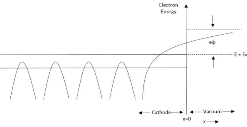
2.11: Energy level diagram for electrons near the surface of a metal between a cathode and vacuum [Reproduced by permission from Author A. S. Gilmour, Jr., Principles of Traveling Wave Tubes, Norwood, MA: Artech House, Inc., 1994. © 1994 by Artech House, Inc.]. ... 32
2.12: Two electrons with sufficient energies to be emitted, but moving in different directions [Reproduced by permission from Author A. S. Gilmour, Jr., Principles of Traveling Wave Tubes, Norwood, MA: Artech House, Inc., 1994. © 1994 by Artech House, Inc.]. ... 33
2.13: Fermi-Dirac distribution function for T = 0 and 1273 K. ... 34
2.14: Electric field pattern established by an electron and its image [Reproduced by permission from Author A. S. Gilmour, Jr., Principles of Traveling Wave Tubes,
Norwood, MA: Artech House, Inc., 1994. © 1994 by Artech House, Inc.]. ... 40
2.15: Energy-band diagram between a metal and surface and a vacuum [44]. ... 41
2.16: Potential distribution with and without electrons from cathode to anode in a parallel-plane diode [Reproduced by permission from Author A. S. Gilmour, Jr.,
xv
Principles of Traveling Wave Tubes, Norwood, MA: Artech House, Inc., 1994. © 1994 by Artech House, Inc.]. ... 42
2.17: Potential near the cathode surface [Reproduced by permission from Author A. S. Gilmour, Jr., Principles of Traveling Wave Tubes, Norwood, MA: Artech House, Inc., 1994. © 1994 by Artech House, Inc.]. ... 43
2.18: Current-voltage relationship with one microperveance. ... 45
2.19: Electron gun design components with identified three regions [Reproduced by permission from Author A. S. Gilmour, Jr., Principles of Traveling Wave Tubes,
Norwood, MA: Artech House, Inc., 1994. © 1994 by Artech House, Inc.]. ... 47
2.20: Parallel electron flow achieved by focusing the electrodes [Reproduced by permission from Author A. S. Gilmour, Jr., Principles of Traveling Wave Tubes,
Norwood, MA: Artech House, Inc., 1994. © 1994 by Artech House, Inc.]. ... 48
2.21: Electron trajectories divergence with (solid lines) and without (dashed lines) electrons [Reproduced by permission from Author A. S. Gilmour, Jr., Principles of Traveling Wave Tubes, Norwood, MA: Artech House, Inc., 1994. © 1994 by Artech House, Inc.]. ... 48
2.22: Parallel flow beam due to the focused electrode at cathode potential [Reproduced by permission from Author A. S. Gilmour, Jr., Principles of Traveling Wave Tubes, Norwood, MA: Artech House, Inc., 1994. © 1994 by Artech House, Inc.]. ... 49
2.23:A spherical diode, where inner and outer diameters represent the cathode and anode, respectively [Reproduced by permission from Author A. S. Gilmour, Jr., Principles of Traveling Wave Tubes, Norwood, MA: Artech House, Inc., 1994. © 1994 by Artech House, Inc.]. ... 50 2.24: Conical diode with half angle [Reproduced by permission from Author A. S. Gilmour, Jr., Principles of Traveling Wave Tubes, Norwood, MA: Artech House, Inc., 1994. © 1994 by Artech House, Inc.]. ... 51
2.25: Low perveance increases the distortion near the anode aperture [Reproduced by permission from Author A. S. Gilmour, Jr., Principles of Traveling Wave Tubes,
Norwood, MA: Artech House, Inc., 1994. © 1994 by Artech House, Inc.]. ... 52
2.26: A higher perveance increases the size of the anode and decreases the distance between the cathode and anode resulting in some distortion near the cathode [Reproduced by permission from Author A. S. Gilmour, Jr., Principles of Traveling Wave Tubes, Norwood, MA: Artech House, Inc., 1994. © 1994 by Artech House, Inc.]. ... 52
2.27: A modified focused electrode to improve the electron gun design by reducing the distortion of equipotential profiles and improving the electron focusing and cathode
xvi
emission uniformity [Reproduced by permission from Author A. S. Gilmour, Jr., Principles of Traveling Wave Tubes, Norwood, MA: Artech House, Inc., 1994. © 1994
by Artech House, Inc.]. ... 53
2.28: Quantities used in the analysis of effect of anode aperture to calculate the gun parameters [Reproduced by permission from Author A. S. Gilmour, Jr., Principles of Traveling Wave Tubes, Norwood, MA: Artech House, Inc., 1994. © 1994 by Artech House, Inc.]. ... 53
2.29: Electron beam shape in region 3 [1]. ... 55
2.30: Cathode-to-anode voltage way to control the beam current in the electron gun [1]. ... 56
2.31: Modulating anode way to control the beam current in the electron gun [1]. ... 57
2.32: Focusing electrode way to control the beam current in the electron gun [1]... 57
2.33: Grid way to control the beam current in the electron gun [1]... 58
2.34: Gun parameters to determine grid-cathode spacing [1]. ... 58
2.35: The effects of space charge and focusing forces on the electron beam [Reproduced by permission from Author A. S. Gilmour, Jr., Principles of Traveling Wave Tubes, Norwood, MA: Artech House, Inc., 1994. © 1994 by Artech House, Inc.]. ... 60
2.36: The use of a solenoid to generate a magnetic field and focus the beam in linear beam tubes [Reproduced by permission from Author A. S. Gilmour, Jr., Principles of Traveling Wave Tubes, Norwood, MA: Artech House, Inc., 1994. © 1994 by Artech House, Inc.]. ... 61
2.37: Configuration of magnetic flux lines as the electron beam enters the solenoid [1]. 61 2.38: Electron trajectory in the axial field [1]. ... 62
2.39: Brillouin flow condition [1]. ... 63
2.40: Resulted beam dynamics when the electron beam enters the magnetic field [1]. ... 63
2.41: Magnetic field configuration for Brillouin flow at the entrance going to the focusing structure [1]. ... 67
2.42: Obtained electron beam if the used magnetic flux density is less than Brillouin flux density [1]. ... 68
xvii
2.43: Beam shape as the magnetic flux density is varied compared to the Brillouin flux
density [1]. ... 69
2.44: Beam shape as the magnetic flux density is varied compared to the Brillouin flux density when db/dz is larger than zero [1]. ... 69
2.45: A system of periodic permanent magnet with a periodic focusing [1]. ... 70
2.46: Difference between a beam ripple and scalloping [1]. ... 71
2.47: Beam envelop curves for three cases of the magnetic field with different values of α and β [89]. ... 73
2.48: Focusing conditions as α and β are varied [1]. ... 73
2.49: Unstable conditions for the normalized beam radius equation based on α values [1]. ... 74
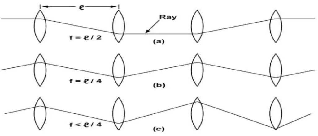
2.50: A series of convergent lenses demonstrating the PPM [1]. ... 74
2.51: Focusing conditions in terms of optical rays for different focal lengths [1]... 75
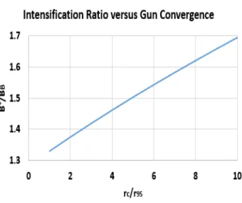
2.52: Intensification factor versus radius compression ratio of the PPM field. ... 78
2.53: Normalized focusing factor versus radius compression ratio of the PPM field. ... 79
2.54: Transmission model for the RF circuit of the TWT. ... 83
2.55: Transmission line model for the RF circuit of the TWT to determine current at point A. ... 83
2.56: Transmission line model for the RF circuit of the TWT to determine the voltages around loop ABCD. ... 84
2.57: Power gain as a function of CN for the synchronous condition in a traveling wave tube. ... 90
2.58: Difference between group and phase velocity [Reproduced by permission from Author A. S. Gilmour, Jr., Principles of Traveling Wave Tubes, Norwood, MA: Artech House, Inc., 1994. © 1994 by Artech House, Inc.]. ... 92
2.59: Opposite directions of the group and phase velocities [Reproduced by permission from Author A. S. Gilmour, Jr., Principles of Traveling Wave Tubes, Norwood, MA: Artech House, Inc., 1994. © 1994 by Artech House, Inc.]. ... 93
xviii
2.60: Illustration of dispersion characteristics between the phase velocity and frequency [Reproduced by permission from Author A. S. Gilmour, Jr., Principles of Traveling Wave Tubes, Norwood, MA: Artech House, Inc., 1994. © 1994 by Artech House, Inc.]. ... 94
2.61: Electric and magnetic fields' lines of a coaxial transmission line in the fundamental TEM mode [Reproduced by permission from Author A. S. Gilmour, Jr., Principles of Traveling Wave Tubes, Norwood, MA: Artech House, Inc., 1994. © 1994 by Artech House, Inc.]. ... 95
2.62: Brillouin diagram for a coaxial transmission line in the TEM mode [Reproduced by permission from Author A. S. Gilmour, Jr., Principles of Traveling Wave Tubes,
Norwood, MA: Artech House, Inc., 1994. © 1994 by Artech House, Inc.]. ... 95 2.θ3: Two plane waves at angles ±α in the z-direction [Reproduced by permission from Author A. S. Gilmour, Jr., Principles of Traveling Wave Tubes, Norwood, MA: Artech House, Inc., 1994. © 1994 by Artech House, Inc.]. ... 96
2.64: Group and phase velocities inside a waveguide [Reproduced by permission from Author A. S. Gilmour, Jr., Principles of Traveling Wave Tubes, Norwood, MA: Artech House, Inc., 1994. © 1994 by Artech House, Inc.]. ... 97
2.65: Wave configurations inside the waveguide for frequencies f1 > f2 > f3 [Reproduced by permission from Author A. S. Gilmour, Jr., Principles of Traveling Wave Tubes, Norwood, MA: Artech House, Inc., 1994. © 1994 by Artech House, Inc.]. ... 98
2.66: Quantities used to derive the dispersion characteristics of a waveguide [Reproduced by permission from Author A. S. Gilmour, Jr., Principles of Traveling Wave Tubes, Norwood, MA: Artech House, Inc., 1994. © 1994 by Artech House, Inc.]. ... 98
2.67: Brillouin diagram for a rectangular waveguide [Reproduced by permission from Author A. S. Gilmour, Jr., Principles of Traveling Wave Tubes, Norwood, MA: Artech House, Inc., 1994. © 1994 by Artech House, Inc.]. ... 99
2.68: Changes in the propagation constant when the angular frequency is varied [Reproduced by permission from Author A. S. Gilmour, Jr., Principles of Traveling Wave Tubes, Norwood, MA: Artech House, Inc., 1994. © 1994 by Artech House, Inc.]. ... 100
2.69: Group velocity from the Brillouin diagram for different wave configurations [Reproduced by permission from Author A. S. Gilmour, Jr., Principles of Traveling Wave Tubes, Norwood, MA: Artech House, Inc., 1994. © 1994 by Artech House, Inc.]. ... 101
2.70: Electric field distributions in the dominant mode in the rectangular waveguide [Reproduced by permission from Author A. S. Gilmour, Jr., Principles of Traveling
xix
Wave Tubes, Norwood, MA: Artech House, Inc., 1994. © 1994 by Artech House, Inc.]. ... 101
2.71: Brillouin diagram in the rectangular waveguide for propagating waves in either direction [Reproduced by permission from Author A. S. Gilmour, Jr., Principles of Traveling Wave Tubes, Norwood, MA: Artech House, Inc., 1994. © 1994 by Artech House, Inc.]. ... 102
2.72: Saturated output power versus frequency for a helix TWT [1]. ... 103
2.73: Effect of harmonic injection on the saturated output power for a helix [1]. ... 103
2.74: Helix being cut at points x and is being straightened [Reproduced by permission from Author A. S. Gilmour, Jr., Principles of Traveling Wave Tubes, Norwood, MA: Artech House, Inc., 1994. © 1994 by Artech House, Inc.]. ... 104
2.75: Ideal Brillouin diagram without dispersion for a helix [1]. ... 104
2.76: Electric field pattern with two different frequencies [Reproduced by permission from Author A. S. Gilmour, Jr., Principles of Traveling Wave Tubes, Norwood, MA: Artech House, Inc., 1994. © 1994 by Artech House, Inc.]. ... 105
2.77: Magnetic flux cancellation between the helix turns [Reproduced by permission from Author A. S. Gilmour, Jr., Principles of Traveling Wave Tubes, Norwood, MA: Artech House, Inc., 1994. © 1994 by Artech House, Inc.]. ... 106
2.78: Brillouin diagram for a helix with a 10° pitch angle [1]. ... 106
2.79: Common techniques used to control the dispersion [Reproduced by permission from Author A. S. Gilmour, Jr., Principles of Traveling Wave Tubes, Norwood, MA: Artech House, Inc., 1994. © 1994 by Artech House, Inc.]. ... 107 2.80: Normalized phase velocity and Pierce’s velocity parameter as a function of
frequency for the suggested techniques to control dispersion [98]... 108
2.81: Small signal gain as a function of frequency for the suggested techniques to control dispersion [98]. ... 108
2.82: Backward wave oscillations on a helix for two turns [Reproduced by permission from Author A. S. Gilmour, Jr., Principles of Traveling Wave Tubes, Norwood, MA: Artech House, Inc., 1994. © 1994 by Artech House, Inc.]. ... 110
2.83: Suppressing BWO with the use of resonant loss to produce attenuation [99]. ... 111
2.84: Saturated output power of a 10 kW helix TWT with a resonant loss at 8 GHz [100]. ... 111
xx
2.85: Technique of pitch change to suppress backward wave oscillations [99]. ... 112
2.86: Peak output power versus midband frequency with BWO suppression techniques and without them [100]. ... 113
2.87: A typical use of support rods with a helix. ... 113
2.88: Interaction impedance of a helix with and without the use of support rods [1]. ... 114
2.89: Thermal conductivities of some dielectric and metal materials [1]. ... 114
2.90: Temperature drop between helix and support rods and between support rods and barrel [99]... 115
2.91: Thermal interface conductivities versus contact pressure for some dielectrics interfaced with a helix made of tungsten [1]. ... 115
2.92: Pressure or hot insertion technique [1]. ... 116
2.93: Comparison between rod support and block support structures [102]. ... 117
2.94: Comparison of the helix temperature with respect to the input power between the triangulation, pressure or hot insertion, and brazing techniques [103]. ... 118
2.95: Quantities used in the analysis of oscillations [Reproduced by permission from Author A. S. Gilmour, Jr., Principles of Traveling Wave Tubes, Norwood, MA: Artech House, Inc., 1994. © 1994 by Artech House, Inc.]. ... 119
2.96: Lossy filum attenuator used with a helix [1]. ... 119
2.97: Use of two severs with a helix to suppress the backward wave and obtain a better efficiency than the attenuator [1]. ... 120
2.98: Ring bar and contrawound helix circuits [1]. ... 120
2.99: Backward wave interactions for a single and bifilar helix [1]. ... 121
2.100: Brillouin diagram for the ring bar structure [1]. ... 122
2.101: Normalized phase velocity for the ring bar structure in the Ka-band frequency range with 18 kV beam voltage [1]... 122
xxi
2.103: Power flow in a linear beam flow [Reproduced by permission from Author A. S. Gilmour, Jr., Principles of Traveling Wave Tubes, Norwood, MA: Artech House, Inc., 1994. © 1994 by Artech House, Inc.]. ... 124
2.104: Collector for a linear beam tube [Reproduced by permission from Author A. S. Gilmour, Jr., Principles of Traveling Wave Tubes, Norwood, MA: Artech House, Inc., 1994. © 1994 by Artech House, Inc.]. ... 126
2.105: Depressed collector circuit to recover the beam power [Reproduced by permission from Author A. S. Gilmour, Jr., Principles of Traveling Wave Tubes, Norwood, MA: Artech House, Inc., 1994. © 1994 by Artech House, Inc.]. ... 126
2.106: Power supply configuration for a multistage depressed collector [Reproduced by permission from Author A. S. Gilmour, Jr., Principles of Traveling Wave Tubes,
Norwood, MA: Artech House, Inc., 1994. © 1994 by Artech House, Inc.]. ... 127
3.1: Quantities used in the analysis of effect of anode aperture to calculate the gun parameters [[Reproduced by permission from Author A. S. Gilmour, Jr., Principles of Traveling Wave Tubes, Norwood, MA: Artech House, Inc., 1994. © 1994 by Artech House, Inc.]. ... 136
3.2: Disc radius of cathode versus cathode emission density for a beam current of 12 A. ... 140
3.3: Sectional view of magnet stack consisting of two magnets and iron pole pieces. .. 141
3.4: A diagram describing the procedure to iterate the angle values until achieving the appropriate electron gun parameters’ calculations. ... 143 3.5: Disc radius of cathode versus cathode emission density relationship from equation (3.1) with a beam current of 50 mA. ... 146
3.6: Disc radius of cathode versus cathode emission density relationship from equation (3.1) with beam currents of 50 mA in red and 1 A in blue. ... 147
3.7: Disc radius of cathode versus beam current relationship from equation (3.1) with cathode emission densities of 2 A/cm2 in red, 10 A/cm2 in blue, 50 A/cm2 in green, and 100 A/cm2 in cyan. ... 147
3.8: Theta versus alpha from equation (2.101) with a beam voltage of 18.2 kV and current of 50 mA. ... 148
3.9: Theta versus alpha from equation (2.101) with a beam voltage of 18.2 kV and current of 50 mA in red, and beam voltage of 10 kV and current of 1 A in blue. ... 148
xxii
3.10: Perveance versus alpha from equations (2.101), (2.84), and (3.2) with different theta values of 30 degrees in red, 20 degrees in blue, 10 degrees in green and 5 degrees in cyan with beam voltage of 18.2 kV and current of 50 mA. ... 149
3.11: Beam voltage versus alpha from equation (2.101) with different theta values of 30 degrees in red, 20 degrees in blue, 10 degrees in green and 5 degrees in cyan with a beam current of 50 mA. ... 149
3.12: Beam current versus alpha from equation (2.101) with different theta values of 30 degrees in red, 20 degrees in blue, 10 degrees in green and 5 degrees in cyan with a beam voltage of 18.2 kV... 150
3.13: Gamma versus alpha constants from equations (3.3-3.4). ... 150
3.14: Gamma versus its derivative constants from equation (3.6). ... 151
3.15: Slope of trajectory for Region 2 versus alpha from equation (3.5) with different values of theta and gamma derivative. ... 151
3.16: Slope of trajectory for Region 2 versus Ra from equation (3.5) with different values of bo, alpha, and gamma derivative. ... 152
3.17: Slope of trajectory for Region 2 versus Ra from equation (3.5) with different values of correction factor, bo, alpha, and gamma derivative. ... 152
3.18: bo versus disc radius of cathode from equation (3.7) with different values of
gamma. ... 153
3.19: bo versus gamma from equation (3.7) with different values of disc radius of
cathode. ... 153
3.20: Slope of trajectory for Region 3 versus minimum beam diameter from equation (3.7) with different values of bo. ... 154
3.21: Slope of trajectory for Region 3 versus bo from equation (3.7) with a beam voltage of 18.2 kV, beam current of 50 mA, and minimum beam diameter of 0.0375 mm. ... 154
3.22: Slope of trajectory for Region 3 versus perveance from equation (3.7) with different values of bo. ... 155
3.23: Spherical radius versus disc radius of cathode from equation (3.9) with different values of theta. ... 155
3.24: Spherical radius versus theta from equation (3.9) with different values of disc radius of cathode. ... 156
xxiii
3.25: Ra versus spherical radius from equation (3.10) with different values of gamma. 156
3.26: Ra versus gamma from equation (3.10) with different values of spherical radius. 157
3.27: ra versus bo from equation (3.11). ... 157
3.28: za versus ra from equation (3.12) with different values of spherical radius and Ra.158
3.29: za versus Ra from equation (3.12) with different values of spherical radius and ra. ... 158
3.30: za versus spherical radius from equation (3.12) with different values of Ra and ra. ... 159
3.31: zm versus minimum beam diameter from equation (3.13) with different values of za and bo. ... 159
3.32: zm versus perveance from equations (3.7) and (3.13) with different values of za and bo. ... 160
3.33: zm versus bo from equation (3.13) with different values of za. ... 160
3.34: zm versus za from equation (3.13) with different values of bo. ... 161
3.35: Diagram representing the overall method used in the gun codes [123]. ... 161
3.36: Electron gun trajectory of the first design for the first electron gun with a beam voltage of 10 kV, beam current of 1 A, and cathode emission density of 2 A/cm2. ... 163
3.37: A zoomed in plot of the electron gun trajectory of the first design for the first electron gun with a beam voltage of 10 kV, beam current of 1 A, and cathode emission density of 2 A/cm2. ... 163
3.38: Electron gun trajectory of the second design for the first electron gun with a beam voltage of 10 kV, beam current of 1 A, and cathode emission density of 2 A/cm2. ... 164
3.39: A zoomed in plot of the electron gun trajectory of the second design for the first electron gun with a beam voltage of 10 kV, beam current of 1 A, and cathode emission density of 2 A/cm2. ... 164
3.40: Electron gun trajectory of the third design for the first electron gun with a beam voltage of 10 kV, beam current of 1 A, and cathode emission density of 2 A/cm2. ... 165
3.41: A zoomed in plot of the electron gun trajectory of the third design for the first electron gun with a beam voltage of 10 kV, beam current of 1 A, and cathode emission density of 2 A/cm2. ... 165
xxiv
3.42: Electron gun trajectory for the proposed novel slow-wave structure of the traveling wave tube with a beam voltage of 262 kV, beam current of 12 A, and cathode emission density of 5.968 A/cm2. ... 166
3.43: Uniform and permanent periodic magnets with respect to the magnetic field
entrance in the placement of the beam waist [95]... 167
3.44: A single period periodic permanent magnet focusing structure [69]. ... 167
3.45: One cell magnet structure consisting of a magnet block, pole pieces, and hubs using ANSYS Maxwell. ... 168
3.46: Parameters of the one cell periodic permanent magnet using ANYSYS Maxwell. ... 169
3.47: Magnetic field profile along one cell of the magnet stack using ANSYS Maxwell. ... 169
3.48: Magnetic field profile along one cell of periodic permanent magnet using ANSYS Maxwell. ... 170
3.49: Periodic permanent magnet with an array of magnet blocks. ... 170
3.50: Magnetic field profile along the periodic permanent magnet stack using ANSYS Maxwell. ... 171
3.51: Magnetic field profile along the array of periodic permanent magnet using ANSYS Maxwell. ... 171
3.52: Final magnetic field profile along the array of periodic permanent using ANSYS Maxwell. ... 172
3.53: Electron gun trajectory and magnetic field plot for the proposed novel slow-wave structure of the traveling wave tube a beam voltage of 262 kV, beam current of 12 A, and cathode emission density of 5.968 A/cm2. ... 173
4.1: A simple coupled inductor circuit. ... 177
4.2: A circuit with three coupled inductors. ... 178
4.3: A simple coupled capacitor circuit. ... 179
4.4: A circuit with three coupled capacitors. ... 181
xxv
4.6: Two lossless transmission lines. ... 183
4.7: Side and perspective views of one-cell of the modeled slow-wave circuit structure of the TWT. ... 187
4.8: Perspective view of one-cell of the modeled slow-wave circuit structure of the TWT surrounded by a circular waveguide. ... 187
4.9: Dimensions of the modeled one-cell slow-wave circuit structure of the TWT. ... 188
4.10: Other dimensions of the modeled one-cell slow-wave circuit structure of the TWT surrounded by a circular waveguide. ... 188
4.11: Available solution types from HFSS menu. ... 190
4.12: Master boundary condition. ... 191
4.13: Slave boundary condition. ... 191
4.14: Assigning the phase delay in the slave boundary condition. ... 192
4.15: Transparent view of the novel slow-wave circuit structure of the TWT design with applied master/slave boundaries. ... 192
4.16: Eigenmode solution setup. ... 193
4.17: Setup sweep analysis. ... 193
4.18: Dispersion diagram of the novel slow-wave circuit structure of the TWT for the early stage designs with the x-axes being in degrees and circular waveguide radius of 54.61 mm. ... 194
4.19: Dispersion diagram of the novel slow-wave circuit structure of the TWT for the early stage designs with the x-axes being in radians and circular waveguide radius of 54.61 mm. ... 194
4.20: Dispersion diagram of the novel slow-wave circuit structure of the TWT for the early stage designs with the x-axes being in degrees and circular waveguide radius of 127.0 mm. ... 196
4.21: Dispersion diagram of the novel slow-wave circuit structure of the TWT for the early stage designs with the x-axes being in radians and circular waveguide radius of 127.0 mm. ... 196
xxvi
4.22: Propagation constant versus frequency of the novel slow-wave circuit structure of the TWT for the early stage designs with a circular waveguide radius of 127.0 mm. ... 197
4.23: Normalized phase velocity versus frequency of the novel slow-wave circuit structure of the TWT for the early stage designs with a circular waveguide radius of 127.0 mm. ... 198
4.24: Normalized phase velocity and interaction impedance versus frequency of the novel slow-wave circuit structure of the TWT for L = 16.0, W = 13.0, p = 22.0 [in mm]. ... 200
4.25: Normalized phase velocity and interaction impedance versus frequency of the novel slow-wave circuit structure of the TWT for L = 14.0, W = 13.0, p = 20.0 [in mm]. ... 201
4.26: Normalized phase velocity and interaction impedance versus frequency of the novel slow-wave circuit structure of the TWT for L = 16.0, W = 15.0, p = 22.0 [in mm]. ... 202
4.27: Normalized phase velocity and interaction impedance versus frequency of the novel slow-wave circuit structure of the TWT for L = 16.0, W = 20.0, p = 22.0 [in mm]. ... 203
4.28: Normalized phase velocity and interaction impedance versus frequency of the novel slow-wave circuit structure of the TWT for L = 15.0, W = 13.0, p = 21.0 [in mm]. ... 204
4.29: Side and perspective views of one-cell of the modeled slow-wave circuit structure of the TWT with L = 15.0, W = 0.0, and p = 21.0 [in mm]. ... 205
4.30: Perspective view of one-cell of the modeled slow-wave circuit structure of the TWT surrounded by a circular waveguide with L = 15.0, W = 0.0, and p = 21.0 [in mm]. .... 205
4.31: Dispersion diagram of the slow-wave circuit structure of the TWT with L = 15.0, W = 0.0, and p = 21.0 [in mm] with the x-axes being in degrees and circular waveguide radius of 127.0 mm. ... 206
4.32: Dispersion diagram of the slow-wave circuit structure of the TWT with L = 15.0, W = 0.0, and p = 21.0 [in mm] with the x-axes being in radians and circular waveguide radius of 127.0 mm. ... 206
4.33: Propagation constant versus frequency of the slow-wave circuit structure of the TWT with L = 15.0, W = 0.0, p = 21.0, and circular waveguide radius of 127.0 [in mm]. ... 207
4.34: Normalized phase velocity versus frequency of the slow-wave circuit structure of the TWT with L = 15.0, W = 0.0, p = 21.0, and circular waveguide radius of 127.0 [in mm]. ... 207
4.35: Interaction impedance versus frequency of the slow-wave circuit structure of the TWT with L = 15.0, W = 0.0, and p = 21.0 [in mm]. ... 208
xxvii
4.36: Comparison between the total area of the slow-wave structure when the width of the transmission lines is not zero at one time and zero at another time. ... 209
4.37: Two parallel transmission lines. ... 210
4.38: Side and perspective views of one-cell of the modeled slow-wave circuit structure of the TWT for L = 16.0, W = 10.5, and p = 22.0 [in mm]. ... 216
4.39: Side and perspective views of one-cell of the modeled slow-wave circuit structure of the TWT for L = 16.0, W = 10.5, p = 22.0, and circular waveguide radius of 127.0 [in mm]. ... 216
4.40: Side and Perspective views of one-cell of the modeled slow-wave circuit structure of the TWT for L = 16.0, W = 10.5, p = 22.0 [in mm] with another pair of shifted
transmission line by 90°. ... 218
4.41: Side and perspective views of one-cell of the modeled slow-wave circuit structure of the TWT surrounded by a circular waveguide for L = 16.0, W = 10.5, p = 22.0 [in mm] with another pair of shifted transmission line by 90°. ... 219
4.42: Side and perspective views of one-cell of the modeled slow-wave circuit structure of the TWT surrounded by a circular waveguide for L = 16.0 mm, W = 10.5 mm, p = 22.0 mm with one and two pairs of transmission lines. ... 219
4.43: Dispersion diagram of the novel slow-wave circuit structure of the TWT for L = 16.0 mm, W = 10.5 mm, and p = 22.0 mm of both designs and beam line with the x-axes being in degrees and circular waveguide radius of 127.0 mm. ... 220
4.44: Dispersion diagram of the novel slow-wave circuit structure of the TWT for L = 16.0 mm, W = 10.5 mm, and p = 22.0 mm of both designs and beam line with the x-axes being in radians and circular waveguide radius of 127.0 mm. ... 220
4.45: Propagation constant versus frequency of the novel slow-wave circuit structure of the TWT for L = 16.0 mm, W = 10.5 mm, and p = 22.0 mm of both designs with a
circular waveguide radius of 127.0 mm. ... 221
4.46: Normalized phase velocity versus frequency of the novel slow-wave circuit structure of the TWT for L = 16.0 mm, W = 10.5 mm, and p = 22.0 mm of both designs. ... 221
4.47: Interaction impedance versus frequency of the novel slow-wave circuit structure of the TWT for L = 16.0 mm, W = 10.5 mm, and p = 22.0 mm of both designs. ... 222
4.48: Gain parameter versus frequency of the novel slow-wave circuit structure of the TWT for L = 16.0 mm, W = 10.5 mm, and p = 22.0 mm of both designs. ... 223
xxviii
5.1: Parameters of one-cell of the periodic permanent magnet of the compact lightweight traveling wave tube [72]. ... 228
5.2: Simulated output power and gain of the compact lightweight traveling wave tube in the frequency range of 2.0-4.0 GHz... 230 η.3: Authors’ work of the simulated output power and gain of the compact lightweight traveling wave tube in the frequency range of 2.0-4.0 GHz [72]. ... 230
5.4: Exporting a geometry from HFSS. ... 232
5.5: Perspective and side views of the geometry of the novel slow-wave structure of the TWT inside HFSS with L = 16.0 mm, W = 10.5 mm, p = 22.0 mm, and N = 20 ... 232
5.6: Side and perspective views of the imported geometry of the novel slow-wave
structure of the TWT inside HFSS with L = 16.0 mm, W = 10.5 mm, p = 22.0 mm, and N = 20 without the circular waveguide. ... 233
5.7: Geometry of the novel slow-wave structure of the TWT inside VSim with L = 16.0 mm, W = 10.5 mm, p = 22.0 mm, and N = 20 without the tube. ... 234
5.8: Geometry of the novel slow-wave structure of the TWT inside VSim with L = 16.0 mm, W = 10.5 mm, p = 22.0 mm, and N = 20 with the tube. ... 234
5.9: Menu inside the 'Setup' window. ... 235
5.10: Menu inside the 'Run' window to run the simulations. ... 236 η.11: Menu inside the 'Visualize' window to view the results from ‘History’... 237 5.12: Menu inside the 'Analyze' window to apply the low pass filter. ... 237
5.13: Menu inside the 'Visualize’ window to view the results after applying the low pass filter from ‘1-D Fields’. ... 238 5.14: Simulated saturated output power and gain of the novel slow-wave structure of the TWT with L = 16.0 mm, W = 10.5 mm, p = 22.0 mm, and N = 20 in the frequency range of 1.85-2.80 GHz. ... 239
5.15: Output power versus input power of novel slow-wave structure of TWT using VSim with L = 16.0, W = 10.5, p = 22.0 [in mm], and N = 20 at 2.40 GHz. ... 240
5.16: Output power versus number of periods of novel slow-wave structure of TWT using VSim with L = 16.0, W = 10.5, p = 22.0 [in mm], and N = 20 at 2.40 GHz. ... 241
xxix
5.17: Novel slow-wave structure of the TWT with unidentical transmission lines. ... 244
5.18: Novel slow-wave structure of the TWT with unidentical periods resulted due to the difference in lengths. ... 245
CHAPTER I INTRODUCTION
The traveling-wave tube (TWT), categorized as one of two major microwave
devices besides klystron, is considered to be an O-type or linear beam tubes. It is capable
of generating power ranging from watts to megawatts based on the radio-frequency (RF)
circuits and can be used from frequencies below 1 GHz to over 100 GHz. The helix RF
circuit is recognized to be used for wideband applications, but with limited power. The
coupled cavity circuit is common for high power applications, but with limited bandwidth.
TWTs have been of interest in a variety of applications reaching over 50% of the sales
volume among all microwave tubes. Various laboratories, industries, and research
organizations are conducting research and development in TWTs in communications,
satellites, radar systems, and electronic countermeasures systems as a final or high power
amplifier transmitting RF pulse or a driver for other amplifiers. This chapter covers a firm
grasp of the early history over the 20th century, classical types of vacuum tubes, and domain
of vacuum tubes. The remainder of the chapter is devoted to an overview of the dissertation.
1.1 Early Milestones of Traveling-Wave Tube
The first developed TWT was invented by an Austrian born engineer named R.
Kompfner in early 1943 [1-7]. He worked at a government based radar British laboratory
and summarized the operation of the first TWT as:
“When the radio frequency power emerging from the helix with the beam switched on was compared with the radio frequency power without the beam, it was found that, at a beam voltage of 2440 volts, there was an increase of 49%, while at a beam voltage of 2200 volts, there was a decrease of 40%.”
2
In late 1942, Kompfner stated that “the basic growing wave principle of the magnetron could be used for amplification of RF signals” [1]. Accordingly, his plan was developing an amplifier considering the sensitivity and noise factor. Such design was compared with
the best available crystal-mixer receivers at that time. The first TWT was built and tested with an electron beam current and voltage of 110 μA and 1.83 kV, respectively. The resulted amplified power was 6 at a frequency of 3.3 GHz with a noise factor of 14 dB.
The design was improved later to reach an amplification of 14 in addition to reduce the
noise factor by 3 dB to reach 11 dB.
However, in his patent, A. Haeff [8, 9], a Russian electrical engineer, earlier
introduced the electron beam and RF circuit interaction in October, 1933. He indicated that
a hollow electron beam deflected as a nearby RF signal propagated on a helical structure.
Haeff also stated that the velocity of the electron beam was equal to the velocity of the
wave on the RF circuit. Such condition results in an existing amplification in the TWT.
However, his recognition lacked to interpret such amplification of the RF wave as it
traveled.
In 1935, K. Posthumus [10], a Dutch electrical engineer, pointed out the conversion
of the electron energy into an amplification of the RF wave by designing a cavity-type
magnetron oscillator. He described such amplification to be caused as a result of the
interaction between the tangential component of the RF wave as it traveled at a velocity
equal to the velocity of electrons.
N. Lindenblad [11], working at Radio Corporation of America, obtained some
amplification over a 30 MHz band at a frequency of 390 MHz in May, 1940, by applying
3
interaction between the electron beam and RF wave on a helix produced a signal amplification on the helix. Lindenblad modified Haeff’s inductive output tube by replacing the cavity resonator with a helix and extending the vacuum envelope of Haeff’s tube. He also introduced the pitch helix and recognized its value such that synchronism is
maintained and the velocity of the wave on the helix was equal to the velocity of the
electron beam being inside the envelope. The amplification was then resulted as the
velocity was reduced. In addition, Lindenblad introduced the use of a helical waveguide
acting as a slow-wave circuit.
It was not until June 27 and 28, 1946, when the helix traveling wave tube was first
announced in public. J. Pierce and L. Field, working at Bell Telephone Laboratories, participated at the Fourth Institute of Radio Engineer’s Electron Tube Conference at Yale. Besides, the British wartime described the work on the helix wave traveling tubes at the
same conference. Pierce and Field indicated the unique features of the helix traveling wave
tubes [12]. In order to support and fix the helix structure, longitudinal insulating rods were
used and positioned accurately. Furthermore, a uniform magnetic field, produced by a
system of solenoids, was used to focus the electron beam. Moreover, layers of colloidal
graphite on the rods were inserted as a technique to suppress backward traveling waves
and oscillations for providing the appropriate loss. Besides, the gain was sacrificed with
reduction at a minimum level by increasing the conductivity of the coating at the midpoint
of helix. That conductivity delivered a dissipation of the unwanted reflected energy
[13-14].
Through the 20th century, the development and exposition of theories and operation
4
have a unified coordination of the traveling wave tube. Some of those noteworthy
contributions are in [15-16].
1.2 Classical Types of Electronics
The electronics-based sources have gained interest throughout the microwave
frequencies and beyond due to the compactness in size and affordability in systems with
integrated devices and circuits. Figure 1.1 shows the approaches to implement systems and
devices with electronics throughout the microwave frequency range and beyond.
Figure 1.1: System implementation with electronics throughout the microwave frequency range and beyond.
In devices, there are two main groups of the electronics-based source: solid-state and
vacuum.
1.2.1 Solid State Devices
The solid-state devices are active or passive depending on the device implemented.
Examples of active devices are transistors. Recently, two different paths categorize the
modern semiconductor active devices: Si technologies and III/V compound technologies.
Some examples of the Si technologies devices are SiGe Heterojunction Bipolar Transistor (HBT) and Si Metal–Oxide–Semiconductor Field Effect Transistor (MOSFET). Some examples of III/V technologies include Heterojunction Bipolar Transistor (HBT) and High
5
diodes. Compared to the active devices, the passive devices work at higher frequencies and
are used for generating and detecting signals. However, they are limited in applications.
Examples of passive devices used for generating signals include resonant tunneling diodes
(RTDs), IMPAct ionization Transit Time (IMPATT), and Gunn diodes. Examples of
passive devices used for detecting signals include Schottky Barrier Diodes (SBDs),
superconductor-insulator-superconductor (SIS) tunnel junction mixer, and hot electron
bolometer (HEB) [17].
1.2.2 Vacuum Devices
Instead of using transistors or diodes, the vacuum electron devices include the use
of vacuum tubes within which the electron beam travels. The kinetic and flow of electrons
are controlled in the tube. The vacuum devices are classified based on the configurations
of the tube as either fast-wave or slow-wave. Examples of fast-wave devices include
gyrotrons and free electron lasers (FEL). In contrast, the electrons travel slower than the
speed of light, c, in the slow-wave devices to synchronize with the wave velocity. Examples
of slow-wave devices include klystrons, magnetrons, traveling wave tubes (TWTs), and
backward oscillators (BWOs) [17].
Other resources classify the vacuum tube types differently based on the electric and
magnetic fields produced by the electrons [1]. Figure 1.2 shows the categories of vacuum
6
Figure 1.2: Categories of vacuum tubes throughout the microwave frequency range and beyond.
As shown in Figure 1.2, the vacuum tubes are divided into three categories: linear-beam,
crossed-field, and fast-wave tubes. The operating principles of all tubes are the same. They
involve an electron beam passing through the tube and a circuit with an electromagnetic
field. Amplifications or oscillations are produced when the electron beam and circuit
interact with each other. Examples of the linear-beam tubes are klystrons and traveling
wave tubes. Figure 1.3 illustrates the basic configuration of the klystron.
Figure 1.3: Basic configuration of a klystron [1].
As shown in Figure 1.3, the electron beam is formed in the electron gun and linearly travels
to the collector passing through the RF circuit. Resonant cavities form the RF circuit
without an electromagnetic coupling between them. The RF input accelerates and
decelerates the electrons existing in the beam. An RF current in the beam is resulted, which
is proportional to the distance the beam travels. Such current is coupled to the intermediate
cavities inducing a signal and producing a field. The coupling is then followed to the output
7
up with the slow electrons. The klystron can achieve an output power level of tens of
megawatts or more and gain of 60 dB or more. However, its bandwidth is limited between
a few percent and 10%.
If a broadband device is desired, the traveling wave tube replaces the klystron.
Figure 1.4 illustrates the basic configuration of the traveling wave tube.
Figure 1.4: Basic configuration of a traveling wave tube [1].
As shown in Figure 1.4, the RF circuit in the traveling wave tube is continuous. Behaving
like a transmission line, the signal moves along the circuit continuously, but at a targeted
velocity near to the velocity of the electron beam passing through it. The bunches of
electrons are formed when the electric and magnetic fields decelerate and accelerate the
electrons. An RF current in the circuit is resulted when the electron bunches pass by the
circuit. Such current causes the amplitude of the RF field to become larger, which in turn,
increases the intensity of electron bunching in the beam. As far as the velocity of the
electron beam continues to be the same as the velocity of the signal, the bunching continues
to grow and becomes more intense. The TWT can achieve an output power level of tens of
watts for broadband devices and hundreds of kilowatts to megawatts for narrowband
devices. The gain can reach up to 50 dB or more. Its bandwidth is between 20% and over
2 octaves.
The second category of vacuum tubes is crossed-field. Basically, the cathode in the
8
toward the RF circuit. The magnetic field is perpendicular to the electric field, which results
in a circular electron path moving around the cathode. The RF circuit acts as an anode. The
electrons are bunched into spoke-like configurations whenever there is an RF field.
Examples of the cross-field tubes are magnetrons and cross-field amplifiers. Figure 1.5
illustrates the basic configuration of the magnetron.
Figure 1.5: Basic configuration of a magnetron [1].
The magnetron is an oscillator. As shown in Figure 1.5, resonant cavities form the RF
circuit with an electromagnetic coupling between them. The cavity structure resonates only
at a single frequency. The RF electric field in adjacent cavities is 180° out of phase. The
RF magnetic field magnetic is coupled to adjacent cavities. The oscillation is reinforced
when a current in the cavity is induced as the electron spoke arrives at each gap. This occurs when “the electron spoke circles about the cathode in synchronism with the rotating field pattern on the anode” [1]. The magnetron can achieve an output power level of multimegawatt range. It can reach an efficiency as high as 88%.
The other example of the cross-field tubes is the crossed-field amplifier. It operates
the same way the traveling wave tube does. However, instead of the formed electron
bunches in the TWT, the electron spokes are formed. Figure 1.6 illustrates the basic
9
Figure 1.6: Basic configuration of a crossed-field amplifier [1].
The electron spokes circle around the cathode. As the wave travels from the input and
output, it grows due to the electric field from the circuit enhancing the bunches in the spoke
resulting in an induced current in the circuit. Such current enhances the electric field. The
crossed-field amplifier can achieve an output power level of tens of megawatts, but the
gain is less than 20 dB.
The third category of vacuum tubes is fast-wave devices. The interaction between
the wave and electron beam in the fast wave devices is different from the other two
categories. In the linear beam and cross-field devices, the operating frequency is
determined by the circuit whose dimensions are determined by the frequency. Thus, the
generated power is inversely proportional to frequency. In the fast-wave devices, the
operating frequency is determined by the magnetic field and cyclotron frequency. The
circuit dimensions are independent of frequency. Thus, the generated power is proportional
to frequency. Examples of the fast wave tubes are gyro-monotrons and gyro-amplifiers.
Figure 1.7 illustrates the basic configuration of the gyrotron oscillator.
10
As shown in Figure 1.7, the electron beam is hollow and electrons are spiral in shape. The
velocity of the electrons is 1.5 to 2 times larger than the axial velocities. The energy of
electrons plays a role in amplifying the electric field.
1.3 Domain of Vacuum Tubes
A significant factor to consider in many applications is the power level. Throughout
the microwave frequency range and beyond, the vacuum tubes prevail the high power high
frequency applications while the solid-state devices are used at low power and frequencies.
Figure 1.8 compares the average power and frequency range of vacuum and solid-state
devices throughout the microwave frequency range and beyond.
Figure 1.8: Average power and frequency range of vacuum and solid-state devices throughout the microwave frequency range and beyond [1].
Other factors are taken into consideration in applications to compare between the
vacuum tubes and solid-state devices such as efficiency, temperature, reliability, and
bandwidth [18]. The vacuum devices, with the appropriate collector technique, is more
efficient than the solid-state devices. Some tubes can exceed an efficiency of 70%. In
addition, the operating temperature of the vacuum devices is higher than the solid-state
devices. Further, most of the satellite applications use the TWT as the amplifier because
11
helix slow-wave structure can achieve a bandwidth of over 2 octaves for the TWT, resulting
in a preferred choice when a large bandwidth is desired.
1.4 Literature Work
Tremendous efforts have been performed earlier to model, design, and fabricate
slow-wave structures of TWT. Some of which are known to be ring-bar structures or
modified versions of ring-bar structures [19-29]. Such studies have been analyzed by
different resources in a variety of aspects. In general, the ring-bar structure provides a high
operating power level compared to the existing other structures such as the helix and
suppresses the backward wave oscillations. However, its bandwidth capability is limited to
10-20% [1-2]. Figure 1.9 shows a conventional ring-bar structure.
Figure 1.9: Ring-bar structure [30].
As shown in Figure 1.9, one-cell consists of two rings connected once by a bar. The
structure has a period, p, and thickness of the ring. It produces a high interaction impedance
and efficiency and requires a large beam radius for high voltages and currents. Later, a
modified ring-bar structures have been implemented such as half-ring helical structure,
ring-loop structure [31], curved ring-bar structure, and wave-ring helical structure. Figures
12
Figure 1.10: Half-ring helical structure [32].
Figure 1.11: Ring-loop structure [33].
Figure 1.12: Ring-loop and curved ring-bar structures [33].
13
As shown in Figure 1.10, one-cell of the half-ring helical structure consists of two-half
loops separated by a distance d. It exhibits the same dispersion characteristics as the
conventional helix, but obtains a higher gain. That is, the maximum saturated power
achieved for this structure in [32] is 1 kW and a higher gain than the conventional helix
designs by 10 dB. Thus, this structure can be used for low power applications. As shown
in Figure 1.11, one-cell of the ring-loop structure consists of two rings connected by an
elliptic bar. Its normalized phase velocity is below 0.25c, which indicates the use of this
structure for low power TWTs. For the curved ring-bar structure in Figure 1.12, one cell
consists of two rings and two curved transmission lines classifying it as a modified
ring-loop structure. It produces a high normalized phase velocity and moderate interaction
impedance, which indicate the use of such structure for high power TWTs. Such structure
produces the highest reported output power of 1.02 MW in the S-band frequency range and
provides a bandwidth of 33%. For the wave-ring helical structure, the output and gain of
the structure are increased compared to the standard helix by increasing the path motion of
the wave and without changing the length and radius of helix. Such structure can be used
for low power TWTs. Table 1.1 states the comparison between the existing designs of the
traveling wave tube including ring-bar structure, half-ring helical structure, ring loop
structure, curved ring-bar structure, and wave-ring helical structure.
Table 1.1: Comparison between the existing designs of the traveling wave tube including ring-bar structure, half-ring helical structure, ring loop structure, curved ring-bar structure, and wave-ring helical structure.
Parameters Ring-Bar Structure Half-Ring Helical Structure Ring-Loop Structure Curved Ring-Bar Structure Wave-Ring Helical Structure Frequency[GHz] Vary (e.g. X-Band, Q-Band) 2.5-3.25 Vary (e.g. 32-38) 1.8-2.4 2.0-4.0 Number of
Elements, N Vary Helix Vary Unknown 26
Structure Area
[mm3] Vary
814x57x57
14 457x37x37 (p=4.0 mm) Peak Output Power [W] Vary 1.0 k (p=8.0 mm), 220 (p=4.0 mm) Low (e.g. 1300) 1.02 M 39.8 Gain [dB] Vary 28.0 (p=8.0 mm), 46.0 (p = 4.0 mm) Vary (e.g. 45) 29.0 28.0 Bandwidth [%] 10-20 25.00 (p=8.0 mm), 23.43 (p=4.0 mm) - 33.0 - Efficiency [%] - 38.7 (p=8.0 mm), 37.0 (p = 4.0 mm) Vary (e.g. 6.1) 25.0 26.5 Circuit Length (Size) [mm] - 814.0 (p=8.0 mm), 457.0 (p = 4.0 mm) - 740.0 140.5 Magnetic Field
Focusing - - - Yes Yes
Loss Pattern - No - No -
Rods Yes - - No Yes
Bar One Straight One Straight One Elliptic Pair Elliptic One Straight
Phase Velocity 0.30-0.45c (7.0-12.0 GHz), 0.31-0.33c (38.0-44.0 GHz) 0.27-0.32c Vary (e.g. 0.15-0.22c for 2.0-3.0 GHz 0.70-0.78 0.11-0.12c Interaction Impedance [Ω] 13-35 (7.0-12.0 GHz), 21-25 (38.0-44.0 GHz) 30-80 Low (e.g. 20-25) 43-65 50-130
Software Used Vary (e.g.
CST) CST - CST CST
Table 1.1 will be revisited and restated in Chapter 5 when the novel slow-wave structure
design is implemented.
1.5 Novelty of Proposed Work
The main objective of this research is to design a novel slow-wave structure of a
TWT, considered as a modified ring-bar structure design, and investigate its performance.
The approach is achieved by modeling the geometry, studying the characteristics based on
15
using VSim code [37]. One-cell of the novel slow-wave structure of the traveling wave
tube consists of two rings connected by two pairs of transmission lines. For the cold-test
simulations, the dispersion behavior, normalized phase velocity, and interaction impedance
of the modeled design are investigated. Such study is described in Chapter 4. For the
hot-test simulations, VSim code is used to compare the output power results to the conventional
structures based on the ease of manufacturing, bandwidth, gain, and efficiency. Such study
is described in Chapter 5.
Neither of the conducted studies, mentioned in Section 1.4, nor ring-bar or modified
ring-bar structures have been reported with the use of VSim code. Such high performance
code, described in details in Chapter 5, computationally runs intensive electromagnetic,
electrostatic, magnetostatic, and plasma simulations of complex shapes by using 3D
conformal Finite-Difference Time-Domain (FDTD) particle-in-cell (PIC) simulations as
implemented in 3D PIC code. It uses multiprocessor parallelization allowing to obtain high
level simulations. Besides, the physical behavior of the TWT is investigated through the
visualization and postprocessing software. The mode spectrum and mode profile data are
accurately obtained with the mode analysis tool. Also, the user can take advantage of other
features such as the time-history postprocessing to examine the fast Fourier Transform and
the instantaneous amplitude and frequency calculations.
Before proceeding to the novel work, an electron gun and periodic permanent
magnet designs are implemented using EGUN code and ANSYS Maxwell, respectively.
Such task is described in Chapter 3. For this design, the specifications and constraints
require creative POLYGON boundary inputs and electrode contours. At one stage, an


![Figure 2.40: Resulted beam dynamics when the electron beam enters the magnetic field [1]](https://thumb-eu.123doks.com/thumbv2/5dokorg/4324087.97688/93.918.263.706.609.919/figure-resulted-beam-dynamics-electron-enters-magnetic-field.webp)
![Figure 2.42: Obtained electron beam if the used magnetic flux density is less than Brillouin flux density [1]](https://thumb-eu.123doks.com/thumbv2/5dokorg/4324087.97688/98.918.248.715.511.754/figure-obtained-electron-beam-magnetic-density-brillouin-density.webp)
![Figure 2.43: Beam shape as the magnetic flux density is varied compared to the Brillouin flux density [1]](https://thumb-eu.123doks.com/thumbv2/5dokorg/4324087.97688/99.918.240.727.115.339/figure-beam-magnetic-density-varied-compared-brillouin-density.webp)
![Figure 2.47: Beam envelop curves for three cases of the magnetic field with different values of α and β [89]](https://thumb-eu.123doks.com/thumbv2/5dokorg/4324087.97688/103.918.191.779.107.301/figure-beam-envelop-curves-cases-magnetic-different-values.webp)
![Figure 2.49: Unstable conditions for the normalized beam radius equation based on α values [1]](https://thumb-eu.123doks.com/thumbv2/5dokorg/4324087.97688/104.918.271.755.721.935/figure-unstable-conditions-normalized-radius-equation-based-values.webp)