Institutionen för datavetenskap
Department of Computer and Information Science
Final thesis
Minimizing memory requirements for
deterministic test data in embedded testing
by
Daniel Ahlström
LIU-IDA/LITH-EX-G–10/006–SE
2010-03-22
Institutionen för datavetenskap
Department of Computer and Information Science
Final thesis
Title
byName
LIU-IDA...
YYYY-MM-DD
Linköpings universitet SE-581 83 Linköping, SwedenLinköpings universitet 581 83 Linköping
Linköping University
Department of Computer and Information Science
Final thesis
Minimizing memory requirements for
deterministic test data in embedded testing
by
Daniel Ahlström
LIU-IDA/LITH-EX-G–10/006–SE
2010-03-29
Supervisor: Mudassar MajeedSupervisor: Urban Ingelsson Examiner: Erik Larsson
På svenska
Detta dokument hålls tillgängligt på Internet – eller dess framtida ersättare –
under en längre tid från publiceringsdatum under förutsättning att inga
extra-ordinära omständigheter uppstår.
Tillgång till dokumentet innebär tillstånd för var och en att läsa, ladda ner,
skriva ut enstaka kopior för enskilt bruk och att använda det oförändrat för
ick-ekommersiell forskning och för undervisning. Överföring av upphovsrätten vid
en senare tidpunkt kan inte upphäva detta tillstånd. All annan användning av
dokumentet kräver upphovsmannens medgivande. För att garantera äktheten,
säkerheten och tillgängligheten finns det lösningar av teknisk och administrativ
art.
Upphovsmannens ideella rätt innefattar rätt att bli nämnd som upphovsman i den
omfattning som god sed kräver vid användning av dokumentet på ovan beskrivna
sätt samt skydd mot att dokumentet ändras eller presenteras i sådan form eller i
sådant sammanhang som är kränkande för upphovsmannens litterära eller
konst-närliga anseende eller egenart.
För ytterligare information om Linköping University Electronic Press se
för-lagets hemsida
http://www.ep.liu.se/In English
The publishers will keep this document online on the Internet - or its possible
replacement - for a considerable time from the date of publication barring
excep-tional circumstances.
The online availability of the document implies a permanent permission for
anyone to read, to download, to print out single copies for your own use and to
use it unchanged for any non-commercial research and educational purpose.
Sub-sequent transfers of copyright cannot revoke this permission. All other uses of
the document are conditional on the consent of the copyright owner. The
pub-lisher has taken technical and administrative measures to assure authenticity,
security and accessibility.
According to intellectual property law the author has the right to be
men-tioned when his/her work is accessed as described above and to be protected
against infringement.
For additional information about the Linköping University Electronic Press
and its procedures for publication and for assurance of document integrity, please
refer to its WWW home page:
http://www.ep.liu.se/© [
Författarens för- och efternamn]
På svenska
Detta dokument hålls tillgängligt på Internet – eller dess framtida ersättare – under
en längre tid från publiceringsdatum under förutsättning att inga extra-ordinära
om-ständigheter uppstår.
Tillgång till dokumentet innebär tillstånd för var och en att läsa, ladda ner, skriva
ut enstaka kopior för enskilt bruk och att använda det oförändrat för ickekommersiell
forskning och för undervisning. Överföring av upphovsrätten vid en senare tidpunkt kan
inte upphäva detta tillstånd. All annan användning av dokumentet kräver
upphovsman-nens medgivande. För att garantera äktheten, säkerheten och tillgängligheten finns det
lösningar av teknisk och administrativ art.
Upphovsmannens ideella rätt innefattar rätt att bli nämnd som upphovsman i den
om-fattning som god sed kräver vid användning av dokumentet på ovan beskrivna sätt samt
skydd mot att dokumentet ändras eller presenteras i sådan form eller i sådant
samman-hang som är kränkande för upphovsmannens litterära eller konstnärliga anseende eller
egenart.
För ytterligare information om Linköping University Electronic Press se förlagets
hemsida http://www.ep.liu.se/
In English
The publishers will keep this document online on the Internet - or its possible
replace-ment - for a considerable time from the date of publication barring exceptional
circum-stances.
The online availability of the document implies a permanent permission for anyone to
read, to download, to print out single copies for your own use and to use it unchanged for
any non-commercial research and educational purpose. Subsequent transfers of
copy-right cannot revoke this permission. All other uses of the document are conditional on
the consent of the copyright owner. The publisher has taken technical and administrative
measures to assure authenticity, security and accessibility.
According to intellectual property law the author has the right to be mentioned when
his/her work is accessed as described above and to be protected against infringement.
For additional information about the Linköping University Electronic Press and its
procedures for publication and for assurance of document integrity, please refer to its
WWW home page: http://www.ep.liu.se/
c
Abstract
Embedded and automated tests reduce maintenance costs for embedded systems installed in remote locations. Testing multiple components of an embedded system, connected on a scan chain, using deterministic test patterns stored in a system provide high fault coverage but require large system mem-ory. This thesis presents an approach to reduce test data memory requirements by the use of a test controller program, utilizing the observation of that there are multiple components of the same type in a system. The program use deterministic test patterns specific to every component type, which is stored in system memory, to create fully defined test patterns when needed. By storing deterministic test patterns specific to every component type, the program can use the test patterns for multiple tests and several times within the same test. The program also has the ability to test parts of a system without affecting the normal functional operation of the rest of the components in the system and without an increase of test data memory requirements. Two experiments were conducted to determine how much test data memory requirements are reduced using the approach presented in this thesis. The results for the experiments show up to 26.4% reduction of test data memory requirements for ITC´02 SOC test benchmarks and in average 60% reduction of test data memory requirements for designs generated to gain statistical data.
Contents
1 Introduction 1
1.1 Testing of Electronic Systems . . . 1
1.2 Embedded Testing . . . 2
1.3 The Context of this Thesis . . . 2
1.4 Motivational Example . . . 3
1.5 Problems Addressed in this Thesis . . . 4
1.6 Brief Description of the Proposed Solutions . . . 5
1.7 Summary . . . 5
1.8 Outline . . . 6
2 Background 7 2.1 Boundary Scan . . . 7
2.2 Related Work . . . 8
3 Software tool for reducing test data memory requirements 11 3.1 The Concatenator Program . . . 11
3.2 Input Data . . . 13
3.2.1 Description File . . . 13
3.2.2 Test Data File . . . 14
3.2.3 Command Line . . . 15
3.3 Output Data . . . 15
3.3.1 Tests With Equal Amount of Test Patterns . . . 15
3.3.2 Tests With Different Amount of Test Patterns . . . 16
3.4 Extensions for Practical Application of the Concatenator Program . . . 16
3.4.1 Converting Output Data to STAPL . . . 16
3.4.2 Program to Evaluate Test Response from a Boundary Scan System . . . 17
4 Experiments 19 4.1 Experiment 1 . . . 19
4.1.1 Description and Test Data Files . . . 20
4.1.2 Result of Experiment 1 . . . 21
4.2 Experiment 2 . . . 23
Bibliography 27
Appendices 29
A Boundary scan 29
A.1 Test Access Port Controller . . . 29
A.2 Boundary Scan Instructions . . . 31
List of Figures
1 A system under test with input and output pins . . . 22 Overview of an embedded system with a test controller . . . 3
3 Test stimuli applied and test response fetched . . . 3
4 Boundary scan cells on the inputs and outputs of a component . . . 4
5 Duplication both in the same test patterns and between test patterns . . . 4
6 The relationship between FDTPs and CTSTPs . . . 5
7 Component employing boundary scan . . . 7
8 The Concatenator program flow chart . . . 11
9 An example system with three components, marked IC1, IC2 and IC3 . . . 12
10 The concatenation process of the Concatenator program shown in step 3 of Figure 8 . . 12
11 Description file . . . 13
12 Test data file . . . 14
13 Output data file . . . 15
14 Output data file with different amount of test patterns . . . 16
15 Flow chart with STAPL conversion . . . 17
16 Overview of an embedded system, with an external test manager . . . 19
17 Program flow for experimentation . . . 20
18 Sorted graph of Experiment 1 results . . . 22
19 TAP finite state machine . . . 29
List of Tables
1 Instruction support of the Concatenator program . . . 142 Experimental setup of the description and test data files . . . 20
3 Experiment 1 results . . . 22
List of Abbreviations
This section presents all abbreviations used in this thesis in alphabetic order. ASIC Application-Specific Integrated Circuit
ATE Automatic Test Equipment BIST Built-in Self-Test
CTSTP Component Type Specific Test Pattern DFT Design for Test
DR Data Register
FDTP Fully Defined Test Pattern GiB Gibibyte (1024 MiB = 1 GiB) IC Integrated Circuit
IR Instruction Register
ITC International Test Conference KiB Kibibyte (1024 bytes = 1 KiB) MiB Mebibyte (1024 KiB = 1 MiB) PC Personal Computer
PCB Printed Circuit Board
PRPG Pseudo Random Pattern Generation SOC System on a Chip
STAPL Standard Test and Programming Language TAP Test Access Port
TCK Test Clock TDI Test Data In TDO Test Data Out TMS Test Mode Select TRST Test Reset
1
Introduction
Electronic systems today can be used in anything from everyday products like washing machines and cars to base stations for mobile phones and TVs. Electronic systems are getting more and more com-plex [1], where a single system can contain several millions of devices, from small simple resistors to advanced integrated circuits (ICs). As people now depend on these electronic systems, the electronic systems have to be reliable.
Electronic systems in operation can become faulty for several reasons including wear-out and over-heating. Electronic systems that are installed in a remote location is hard to access and the environment in which it is located can be difficult to reproduce. The same system design may also be installed in different kinds of environments and therefore act different. To test remotely located systems, embed-ded and automated tests are used since it tests the system in the environment it operates in. This thesis concerns the high memory requirements, in the order of gibibyte (GiB) [2], for storing test data for embedded test of printed circuit boards (PCBs) or system on a chip (SOC). The thesis deals with this high requirement of memory by applying an approach to reduce redundancy of test data. As will be shown in this thesis test data may be redundantly stored because the circuit under test may contain multiple instances of the same type of component (IC or core) and so the same test data is redundantly stored for each instance of the component.
In particular this thesis considers systems that are tested using deterministic test data that is stored in an embedded memory. The system can be a PCB with multiple IC components or a SOC with multiple core components. In the remainder of this thesis the word system will refer to a PCB or a SOC and the word component will refer to an IC on the PCB or a core in the SOC.
This chapter starts the thesis by presenting the overview of electronic systems, their complexity, the environment in which they reside, the need to perform testing and the motivations to embed the test circuitry in the system. Furthermore this chapter presents an overview of problems in the domain of embedded tests and their solutions.
1.1
Testing of Electronic Systems
A key requirement for obtaining reliable electronic systems is the ability to determine that the systems are error-free [3]. To monitor that a system is working and continues to work according to specifica-tions, testing is required. Testing refers to the verification of manufacturing correctness such that there is no detectable defect in the system. A defect is a deviation from the intended physical structure of the system. Physical defects are modelled as faults according to their effects on a system’s behaviour.
To test a digital electronic system, which is the type of system considered in this thesis, a set of test patterns are applied. Test patterns consist of test stimuli (ones and zeros) and corresponding fault-free test responses (ones and zeros). Test stimuli can be generated randomly, exhaustively or deterministically. The stimuli are applied on the input pins of the system under test and the test response on the output pins of the system is compared with the corresponding response of a fault-free system. Figure 1 shows an overview of a system under test with test stimuli at the input pins and corresponding test response at the output pins.
On a system, the input pins and output pins of the components can be difficult to access for testing. For example, the input pins of one component might only be accessible through another component or the physical density of the system can make access difficult. To provide test access to all input pins and output pins in a system, many systems employ a form of test-specific infrastructure, which is used to transport test data (test stimuli and test response) to and from the inputs and outputs of the systems components. One such infrastructure type is called boundary scan (Section 2.1).
System under test Output pins Input pins Test stimuli vector Test response vector 0 0 1 1 1 0
Figure 1: A system under test with input and output pins
To measure the effectiveness of the test patterns in detecting faults, fault coverage is used as a metric. Fault coverage is the number of faults that can be detected by the test patterns divided by the number of detectable faults i.e. the percentage of faults that can be detected.
With the increasing complexity of electronic systems, the cost and time to test these systems in-crease. Automatic testing is used to reduce the cost and time needed. To automate tests, an external circuit can be used, which can be referred to as automatic testing equipment (ATE). An ATE is used to apply test stimuli on the system under test and to compare the test response with a fault-free test response from the system.
1.2
Embedded Testing
Embedded testing is important since a system that is installed in a remote location is hard to access. With Embedded testing the system is tested in the environment it operates in, which makes it possible to detect defects that only manifest as faults in a particular operating environment.
To aid the testing, some hardware can be added to the design of a system, which is called design for test (DFT). DFT techniques such as scan path design, built-in self-test (BIST) and boundary scan add test-specific circuitry to a system design. DFT include design modifications that provide improved access to internal component elements of a system such that the local internal state can be controlled and/or observed. In BIST, the component controlling the circuitry is required to perform a test on the component itself. The application of test patterns and capturing of results are both done in the internal system and not by external test equipment like in ATE-based testing. In BIST, test stimuli can be generated at the time of test using a pseudo-random test stimulus generator. Alternatively deterministic test patterns can be employed but in this approach, the test patterns must be stored in system memory. In this thesis, a BIST approach with deterministic test patterns is considered.
1.3
The Context of this Thesis
In this section, the context for this thesis is presented. This thesis deals with the high memory require-ments for storing predefined deterministic test data for embedded test of digital electronic systems.
This thesis assumes a system with at least two components. In the trivial case of only one com-ponent, no reduction of test data memory requirements will be gained by using the proposed method. Figure 2 shows a PCB with three components and a test controller. The test controller contains an embedded processor marked CPU and an embedded memory. The components are connected with the embedded processor, marked by arrows. The arrows represent a serial interface, which can be a
PCB Test Controller
CPU Memory
Component 1 Component 2 Component 3
Figure 2: Overview of an embedded system with a test controller
boundary scan chain (Section 2.1). The memory represents the storage of the deterministic test patterns used to test the components.
Scan-in 1 Scan-out 1 Scan-in 2 Scan-out 2 Scan-in 3 Scan-out n A pp ly A pp ly A pp ly A pp ly
Figure 3: Test stimuli applied and test response fetched
In short, a test is conducted as follows. The test patterns stored in memory are fetched one by one by the processor. If any modifications, such as using the method proposed in this thesis, are needed to a predefined deterministic test pattern, the embedded processor apply the changes to create a fully defined test pattern (FDTP) before applying the FDTP to the serial interface. A FDTP is a test pattern with the length of the whole serial interface of the system. As can be seen in Figure 3, the test stimuli is applied to the serial interface at the same time as a test response from a previous test stimuli vector is fetched from the other end of the serial interface. The response is evaluated by the program that is running on the processor by comparing the response with the expected fault-free response and any faults are noted.
1.4
Motivational Example
A system is equipped with three components (Figure 2). Component 1 has a scan chain length of 15 and use 20 test patterns. Components 2 and Component 3 are of the same type and have a scan chain length of 10 and use 15 test patterns. A scan chain is a serial interface for all components where every fully defined test pattern (FDTP) consists of one test pattern for each component. To test these components with deterministic FDTPs a total number of 15 · 20 + 2 · 10 · 15 = 600 bits is required. As can be seen by the observation of that multiple components are of the same type, multiple components of the same type lead to duplication of stored test data, which is ineffective. This observation is utilized in the method proposed in this thesis, to reduce test data memory requirements. The method would only need 15 · 20 + 10 · 15 = 450 bits to store the deterministic test patterns, which is a reduction of 25%.
If for example a fault was detected in Component 3, more testing may be needed to that component to pin-point the defect. In this case it would be desirable to store a second set of FDTPs to specifically test Component 3. Note that, to store a second set of FDTPs would store a second set of the same test data. Special tests to explicitly test Component 3 do not need to be stored in memory and the test previously performed can be applied again without additional storage and without affecting the other
components in the system. This will further improve the memory requirement statistics in favour of the proposed method and lets the system to continue in operation while testing parts of it.
1.5
Problems Addressed in this Thesis
In this thesis the boundary scan interface have been used, which is a serial interface. In boundary scan the inputs and outputs of all system components are equipped with scan cells consisting of flip-flops that form a shift register, called a scan chain (Figure 4), during test made. Since there is often only one boundary scan shift register on the system, a fully defined test stimuli vector have to be applied to fill the length of the scan chain to make sure that all appropriate scan cells are set correctly. When testing
Scan Chain
Input Scan ChainOutput Scan Cells
Component
inputs 1 Component outputs
11
1
0
0 0
Component
Figure 4: Boundary scan cells on the inputs and outputs of a component
a boundary scan testable system with several components in the system, the test patterns can be very long, hundreds of thousands of bits. The long test patterns occur because all components are connected on the same boundary scan chain. When several components are connected on the same scan chain, duplication of data may occur in the test patterns, especially if two or more components are of the same type. Duplication can occur in the same test pattern and/or between test patterns, as shown in Figure 5 (X, Y and Z refers to different parts of FDTPs). If a test pattern only is used to test a single component, the same part of a test pattern may occur in a test pattern used when the component is tested together with one or more other components in the system. As can be seen by this reasoning, test data can be stored inefficiently.
X Y Y
X Z Z
Fully defined test pattern
Figure 5: Duplication both in the same test patterns and between test patterns
As mentioned above, the same part of a test pattern may be used to test a single component alone or together with one or more other components. Not only can the test patterns be stored inefficiently but they can also lack flexibility. In this thesis the meaning of flexibility is that test patterns can be applied in a different order or components can be tested individually by using the same deterministic test patterns. If not all of the components in a system is tested at the same time, many testing methods need to take all components out of operation even if some are not part of the test.
1.6
Brief Description of the Proposed Solutions
As opposed to store fully defined test patterns (FDTPs) (Figure 6(a)), this thesis proposes a method that can be used to reduce test data volume and increase the flexibility. The method is based on a test controller software tool called Concatenator that runs on an embedded processor with an embedded memory connected to it (Figure 2).
The method will concatenate component type specific test patterns (CTSTPs) on demand to FDTPs, as shown in Figure 6(b). A CTSTP is a test pattern used to test a specific type of component. The CTSTPs will be assembled into FDTPs. By storing CTSTPs, the amount of test data that needs to be stored in the embedded memory can be reduced. Since no CTSTP is stored more then once the redundancy is reduced. The test controller software tool adds flexibility by concatenating the CTSTPs depending on given commands. The commands can be issued either from a remote terminal or from a scheduled test cycle in the system.
Concatenator Type A Type B
Type B
Type A Type A Type B
Component type specific test patterns Fully defined test patterns Fully defined test patterns (a) FDTPs is needed Concatenator Type A Type B Type B
Type A Type A Type B
Component type specific test patterns Fully defined test patterns Fully defined test patterns (b) CTSTPs is used to create FDTPs
Figure 6: The relationship between FDTPs and CTSTPs
The flexibility in the proposed method can be used to test select components or parts of the system while the rest of the system continues in normal operation. If a system can continue to operate without certain components, testing these certain components will reduce downtime due to testing and increase the overall uptime.
The requirements to perform a test with the proposed method are a system with a processor, a suffi-ciently large memory and a communication line from the system to a system maintenance headquarters. A communication line to the system can be useful for issuing specific commands. How large memory that is needed depends on how large and how many test patterns that are used. Also the test control program uses a part of the memory.
Two experiments have been conducted to evaluate the amount of memory reduced by the method proposed in this thesis. The experiments are described in detail in Chapter 4.
1.7
Summary
In this introduction section, the importance of reliable electronic systems has been discussed. To de-termine if an electronic system is reliable, the system has to be tested regularly. Since many electronic systems are placed remotely, regular testing has to be automated and thus embedded into the system. With automated embedded testing, new methods have been created to fully automate the testing se-quences. In Section 1.2, a few different methods were discussed. In this thesis the main focus is on testing embedded systems with predefined deterministic test patterns. The general problem when using deterministic test patterns is the large test data volume for which dedicated system memory resources
is required. This thesis provides a solution to the growing test data volume. This solution is based on a test control software tool running on an embedded processor together with an embedded memory. The software tool reduce the test data volume by reducing the redundancy in the test data stored in the embedded memory and adds a flexibility feature to further enhance the usability of the test data.
1.8
Outline
Next chapter covers previous work done in the area of embedded testing and an introduction to where and how test patterns are used, with an introduction to boundary scan. Chapter 3 give more details on how the test control software tool works and its main features. Two experiments to get statistical information of how well the software tool performs are presented in Chapter 4. The thesis ends with a conclusion and a short discussion on future work in Chapter 5.
2
Background
This chapter provides an access mechanism to test the internal parts of the system under test, namely boundary scan. In related work, the approaches for embedded testing of circuits and SOCs by using an embedded processor with deterministic test patterns stored in an embedded memory are discussed.
2.1
Boundary Scan
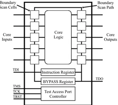
Boundary scan is a standardized method to test interconnects and logic of components. Boundary scan makes it possible to control inputs and outputs on certain components. To accomplish this, boundary scan is implemented by three mandatory registers and a finite state machine called test access port (TAP) controller, controllable by a protocol of five signals. The three mandatory registers are a boundary scan register, an instruction register (IR) and a bypass register, where all are linear shift registers.
The TAP controller controls which of the three registers test data input is shifted into, either the IR, the bypass register or the boundary scan register. By shifting in an instruction into the IR, boundary scan will be set to a test mode (Appendix A.2) equal to the instruction. If the test mode is bypass, the bypass register will be used to connect test data in (TDI) and test data out (TDO) and the component will continue in normal functional mode. The bypass register have a length of a single bit and is used to reduce unnecessary overhead when shifting in test stimuli to other components in the system. If the component is set to any other test mode, the boundary scan register will be connected between TDI and TDO. Test stimuli is shifted into the boundary scan register to set the values of the boundary scan cells, which in turn force input and output pins to the values of the boundary scan cells.
Core Logic Boundary
Scan Cells BoundaryScan Path
Instruction Register BYPASS Register
Test Access Port Controller Core
Inputs OutputsCore
TDO TMS
TCK TRST TDI
Figure 7: Component employing boundary scan
Figure 7 shows the five signals of the boundary scan protocol, the core inputs and outputs, the boundary scan cells, a boundary scan chain and the core logic of a component employing boundary scan. Core logic refers to the processing logic of a component. The boundary scan chain connects the boundary cells, which in turn is connected to the core inputs and outputs. The five signals of the boundary scan protocol, TDI, TDO, TCK, TMS and TRST, are described below.
TDI, test data in, is connected to the in-pin of the boundary scan chain. TDI is the signal where instruction, bypass and boundary scan register values are applied.
TDO, test data out, is connected to the out-pin of the boundary scan chain. While TDI is shifted into a register, the binary values currently in the register are shifted out through TDO.
TCK, test clock, is a clock to control the boundary scan component under test. TCK is used since the internal clock, controlling the components at normal operation, is often too fast and may not be synchronized with the test controller. A slower and synchronized clock is needed to make sure that the boundary scan test is controlled properly.
TMS, test mode select, is controlling the finite state machine of the TAP controller. TRST, test reset, is an optional signal used only to asynchronous reset the TAP controller.
As discussed above, boundary scan is used to access inputs and outputs of components in embedded systems. Boundary scan is implemented as several shift registers between TDI and TDO. In this thesis boundary scan is assumed to provide access to components of a system. The components are assumed to imply a long shift register which is used to apply test stimuli vectors containing test data from all components. More information about the TAP controller and boundary scan instructions are found in Appendix A.
2.2
Related Work
The goal for this thesis is embedded testing of multiple components using deterministic test patterns stored efficiently in an embedded memory with an embedded processor as test controller. There has been considerable research on related areas like embedded testing using compression of deterministic test patterns [4–6] and with reduction of test data volume and test application time [7], built-in self-test (BIST) with pattern generation [8, 9] and/or deterministic patterns [10–12], multi-site testing (using ex-ternal testers), reduction of test data volume and test application time for application-specific integrated circuits (ASICs) with multiple identical cores [13], and embedded software based self-testing [14, 15]. None of the above approaches address all the concerns of this thesis as will be shown in this section.
The main concerns of this thesis are reduction of memory requirements to store deterministic test patterns and to test multiple components at the same time. To address these concerns, this section re-views existing work in the literature related to memory requirements and embedded testing of multiple components in a system.
There are three alternative approaches to deliver test stimuli to the tested system. These three approaches are (1) transporting test stimuli from a source external to the tested system, which is done typically in manufacturing testing, (2) generating the test stimuli on the system (pseudo-random pattern generation, PRPG) [8–12] and (3) storing test stimuli on the system. The first and second approaches share the benefit that no test data needs to be stored on the system. This thesis considers the third approach where test stimuli are stored on the system because the thesis is only concerned with systems that are tested in-field far from any test pattern source. This rules out the first approach, and because the second approach can only generate random test stimuli which are less effective in detecting faults [10] than the deterministic test stimuli [10–12] that can be stored on the system using the third approach. Furthermore, the problems addressed in this thesis (Chapter 3) are found in the domain of systems that employ the third approach by storing deterministic test patterns on the system. In such systems, the amount of dedicated embedded memory required to store the test data (test stimuli and fault-free test responses) is considered a cost. This total amount of test data is called the test data volume. The test data volume can be in order of GiB, which can be seen in [2] where a single component has a test data volume of 0.23 GiB alone. To reduce the test data volume, previous studies have proposed various
test data compression methods [4–6] which reduce the memory requirements for storing the data, but require some processing or dedicated circuitry for expanding the test data to its original form before it is applied to test the components. This thesis provides a method for reducing memory requirements without compression. The author of this thesis however believes that compression of test data can be useful to complement the approach presented in this thesis, which remains to be verified in experiments. Testing of multiple cores has been done in [13]. The technique in [13] reduces the test effort for ASICs with multiple identical cores. The technique generates test data once for identical blocks using PRPG. The technique evaluates tests by comparing responses from the different cores. The comparison is made bit by bit by specialized hardware and if not all bits are the same for each comparison a fault is detected. The evaluations of the tests are therefore dependent on multiple identical cores. The evaluation of test responses used with the method proposed in this thesis does not depend on identical cores and will not need specialized hardware.
To summarize the above literature review, determinism in test patterns achieves high fault coverage but the test patterns need to be stored in a memory. PRPG removes the need of a memory and generates and applies test stimuli when needed and supports in-site testing, but fault coverage tends to be lower. Furthermore compression of test patterns reduces memory requirements but require dedicated hardware or some processing.
As can be seen from the above review of previous research, all previous studies have either focused on manufacturing tests using ATE, compression, PRPG or the observation that test data for identical blocks only need to be stored once [13] to reduce memory requirements. The previous studies have also addressed how to deliver test data to a system for embedded testing, but no previous study has con-sidered the combination of how to store deterministic test patterns for embedded testing while applying the observation from [13] to multiple cores. This motivates the study presented in this thesis as this thesis focuses on in-site embedded testing of multiple components with efficiently stored deterministic test patterns.
3
Software tool for reducing test data memory requirements
This chapter presents a solution to reduce redundancy of test data stored in an embedded memory based on the observation that if a system contains several instances of the same component type only one set of test data is required to be stored for that component type.
The first part explains the software tool by an example. The chapter continues with a more detailed look at the input and output of the software tool.
3.1
The Concatenator Program
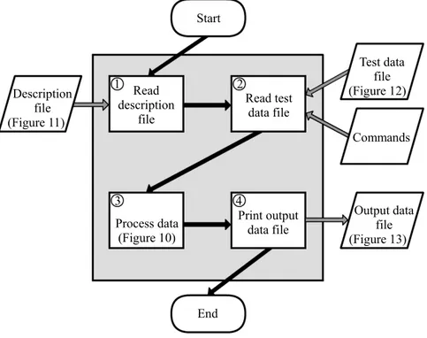
This section explains the software tool, called the Concatenator program. The Concatenator program is divided into four steps (Figure 8). First step is to read a description file of the boundary scan compo-nents within the system. The description file contains the order of the compocompo-nents on the scan chain, which type the components are and information for each type of component; boundary scan register length, instruction register length and available boundary scan instructions with their code words. Sec-ond step is to read and select the component specific test sets used for a particular test from a test data file, based on given commands. Third step is to process the data read and last step is to respond with the fully defined test patterns (FDTPs) created, written into an output file.
3 4 2 1 Read test data file Read description file Process data (Figure 10) Print output data file End Start Test data file (Figure 12) Commands Output data file (Figure 13) Description file (Figure 11)
Figure 8: The Concatenator program flow chart
This part will explain the program flow by an example. The example system (Figure 9) is equipped with three components connected on a boundary scan chain. The first component in the scan chain, marked IC1, is of type A and the two other components, marked IC2 and IC3, are of type B. Figure 10 shows the concatenation method to create fully defined test patterns from component specific test sets. The component specific test set marked Type A Intest 2 are specific to component IC1 and the test set marked Type B Intest 1 are specific to components IC2 and IC3.
The description file (Figure 11) read in step one (Figure 8) is a description of the example system (Figure 9). In this example, the description includes on line 1 the order on the scan chain, IC1, IC2 and
Output
Input IC1 Type A
IC2
Type B Type BIC3
Figure 9: An example system with three components, marked IC1, IC2 and IC3
15 bits
10 bits
15 bits 15 bits 10 bits 10 bits
Test stimuli 1 Test stimuli 1 Test stimuli 1 Test stimuli 3 0 0 Test stimuli 1 Test stimuli 2 Test stimuli 3 Test stimuli 4 Test stimuli 1 Test stimuli 2 Type B Intest 1 Type A
Intest 2 Test IC1 Intest 2, IC2 Intest 1, Command: IC3 Intest 1
Fully defined test stimuli vector
Figure 10: The concatenation process of the Concatenator program shown in step 3 of Figure 8 IC3, with IC1 as first component. The description file also specifies that IC1 is of type A, and IC2 and IC3 is of type B on line 2 and 3. The boundary scan register lengths are also specified, 15 bits for type A and 10 bits for type B.
The command and the test data file read in step two can be seen in Figure 10. The command decides if a component specific test set should be included in the fully defined test patterns or not, if not, the test set are not read. In this example, both test sets are read and Type B’s test set is read twice, Intest 2 is applied to IC1 and Intest 1 is applied to IC2 and IC3. The command is described in detail in Section 3.2.3.
In step three, the test sets are controlled and the appropriate instructions are set for each component. In this example, each test pattern is controlled to be of the right length, 15 bits for type A and 10 bits for type B. The instructions are all set to the INTEST instruction.
Step four prints the fully defined test patterns to a file. As seen in Figure 10, the first test pattern in each test set are merged to the first fully defined test pattern, the second test pattern in each test set to the second fully defined test pattern, and so on.
A more detailed look at the input and output data follows in the sections below. The examples in the following sections are related to the example above.
3.2
Input Data
The input data consist of three parts, a description file (Section 3.2.1), a test data file (Section 3.2.2) and commands (Section 3.2.3).
3.2.1 Description File
In this section the description file format used by the Concatenator program is shown and explained. A description file contains essential information regarding the boundary scan chain and the components in the scan chain.
TypeA INTEST TypeB INTEST 1 IR: 00000111110000111100001111
2 11110000111100001010101010101010101 11100011100011101101101100110110110 3 00001111000011110101010101010101010 00011100011100010010010011001001001 TypeA INTEST1 TypeB INTEST1 TypeA INTEST1 TypeB INTEST1 Test stimuli Expected response
1 IR: 00000111110000111100001111 2 10010010010010001010101010101010101 01010101101010101101101100110110110 3 01101101101101110101010101010101010 10101010010101010010010011001001001 4 IR: 00000111111111111111111111 5 10110111011110100 00000001111111100 6 01001000100001000 11111110000000000
1 IC1 - IC2 - IC3 2 TypeA = IC1
3 TypeB = IC2 = IC3 4 5 TypeA DRLENGTH 15 6 TypeA IRLENGTH 10 7 TypeA IDLENGTH 12 8 TypeA IDCODE 0001011001 9 TypeA vIDCODE 010011011101 10 TypeA vIDCODE 010011011101 11 TypeA BYPASS 1111111111 12 TypeA EXTEST 0000000000 13 TypeA SAMPLE 0001010101 14 TypeA IR_CAPTURE 0101010101 15 TypeA INTEST 0000011111 16 17 TypeB DRLENGTH 10 18 TypeB IRLENGTH 8 19 TypeB BYPASS 11111111 20 TypeB EXTEST 00000000 21 TypeB SAMPLE 00000010 22 TypeB IR_CAPTURE 10000001 23 TypeB INTEST 00001111
Figure 11: Description file
The first line of a description file describes the order of the components. In the example, shown in Figure 11, there are three components, IC1, IC2 and IC3, as can be seen on the first line. In this example IC1 is the first component in the boundary scan chain.
Next, on line 2 and 3, the file contains the description of the type of the components. There is one line for each component type, which gives the list of components that are of the given type. In this example, IC2 and IC3 are of the same type. These type declarations come before the detailed information given for each component type. The detailed information of each component type includes length of boundary scan register, length of instruction register and available boundary scan instructions with their code words.
Instruction Meaning
EXTEST Used to test the interconnects between components. INTEST Used to test the logic of the component.
BYPASS Used to bypass a component by using the bypass register instead of the boundary scan chain to reduce unnecessary overhead. The component remains in its normal functional mode [16]. SAMPLE/PRELOAD Used to take a sample of the functional data entering and
leaving the component. Can also be used to preload data
into the boundary scan register prior to an EXTEST instruction. IR_CAPTURE Used to check if the instruction register of a component
is working correctly.
IDCODE Used to fetch the ID code of a component. Table 1: Instruction support of the Concatenator program 3.2.2 Test Data File
This section shows and explains the test data file format.
TypeA INTEST1 2 111100001111000 111000111000111 000011110000111 000111000111000 TypeA INTEST2 4 100100100100100 010101011010101 011011011011011 101010100101010 101101110111101 000000011111111 010010001000010 111111100000000 TypeB INTEST1 2 0101010101 0110110110 1010101010 1001001001 TypeB INTEST2 4 1111111111 1111111111 0011111100 1111001111 0000110000 1100000011 0000000000 0000000000
Figure 12: Test data file
As seen in the example of a test data file (Figure 12), the file consists of component type specific test sets, which are named with a component type, a test id and the number of component type specific test patterns (CTSTPs) in the test set. The test id consists of an instruction name (for more details see Table 1 and Appendix A.2) and an identifier, where the identifier is used to separate different tests which are to be run with the same instruction. The instruction code is found in the description file (Figure 11). A test id is not component type specific, which means that the same test id can be used for many different test sets.
After the line that names each component type specific test set follows the corresponding CTSTPs. The CTSTPs have two parts, which are stored on the same line separated by a blank-space character. The first part is the test stimuli and the second part is expected test response of a fault-free component.
3.2.3 Command Line
This example will show how to command the Concatenator program of an intest on all three compo-nents, based on the description file (Figure 11) and the test data file (Figure 12). INTEST1 is used for all three components.
The command line will then look like:
concatenator.exe Description.txt Testdata.txt Outdata.data IC1 INTEST1 IC2 INTEST1 IC3 INTEST1
The command line consists of the program command followed by three file paths and pairs of test commands.
The three file paths are Description.txt which is the path to a description file (Section 3.2.1 and Fig-ure 11), Testdata.txt which is the path to a test data file (Section 3.2.2 and FigFig-ure 12) and Outdata.data which is the path to an output file (Section 3.3 and Figure 13).
A test command pair consists of an id of a component to be tested and which test to apply to that device. For example, in the example above, IC1 is the id of a component and INTEST1 is the test applied to IC1.
3.3
Output Data
The output data file consists of two parts, the instruction for the boundary scan protocol (Appendix A.2) and the fully defined test patterns for the considered components in the boundary scan chain, which is created from input data with the Concatenator program (Section 3.1).
3.3.1 Tests With Equal Amount of Test Patterns
The output data file below (Figure 13) is the output created from using the description file (Figure 11), test data file (Figure 12) and commands (Section 3.2.3) from previous examples.
TypeA INTEST TypeB INTEST 1 IR: 00000111110000111100001111
2 11110000111100001010101010101010101 11100011100011101101101100110110110 3 00001111000011110101010101010101010 00011100011100010010010011001001001 TypeA INTEST1 TypeB INTEST1 TypeA INTEST1 TypeB INTEST1 Test stimuli Expected response
1 IR: 00000111110000111100001111 2 10010010010010001010101010101010101 01010101101010101101101100110110110 3 01101101101101110101010101010101010 10101010010101010010010011001001001 4 IR: 00000111111111111111111111 5 10110111011110100 00000001111111100 6 01001000100001000 11111110000000000
1 IC1 - IC2 - IC3 2 TypeA = IC1
3 TypeB = IC2 = IC3 4 5 TypeA DRLENGTH 15 6 TypeA IRLENGTH 10 7 TypeA IDLENGTH 12 8 TypeA IDCODE 0001011001 9 TypeA vIDCODE 010011011101 10 TypeA vIDCODE 010011011101 11 TypeA BYPASS 1111111111 12 TypeA EXTEST 0000000000 13 TypeA SAMPLE 0001010101 14 TypeA IR_CAPTURE 0101010101 15 TypeA INTEST 0000011111 16 17 TypeB DRLENGTH 10 18 TypeB IRLENGTH 8 19 TypeB BYPASS 11111111 20 TypeB EXTEST 00000000 21 TypeB SAMPLE 00000010 22 TypeB IR_CAPTURE 10000001
Figure 13: Output data file
In the output data file (Figure 13) the first line precedes of “IR:” which indicate that this line is to be read as an instruction and the second argument is the instruction. The following lines consist of FDTPs concatenated by the program. As in the test data file (Figure 12) the first group of bits are test stimulus and the second group of bits are expected test responses. If an instruction or test stimuli of the wrong length is applied, the response may be wrong because of that. The program checks that the instruction and the test patterns is of the right length before being printed. The check is performed by comparing the length of the test patterns to data in the description file (Figure 11).
3.3.2 Tests With Different Amount of Test Patterns
The number of test patterns in a component type specific test set will depend on the component, differ-ent tests will therefore in many cases have differdiffer-ent amount of test patterns. A feature of the Concate-nator program is to concatenate test sets with different amount of test patterns. This can for example be useful if one or more components need more extensive testing then the rest of the components or different tests are applied at the same time.
In this example, component IC1 will use INTEST2 from the test data file (Figure 12), while com-ponents IC2 and IC3 still use INTEST1.
The command line in this example looks like:
concatenator.exe Description.txt Testdata.txt Outdata.data IC1 INTEST2 IC2 INTEST1 IC3 INTEST1
The command above creates an output data file that looks like the one below (Figure 14).
TypeA INTEST TypeB INTEST 1 IR: 00000111110000111100001111
2 11110000111100001010101010101010101 11100011100011101101101100110110110 3 00001111000011110101010101010101010 00011100011100010010010011001001001 TypeA INTEST1 TypeB INTEST1 TypeA INTEST1 TypeB INTEST1 Test stimuli Expected response
1 IR: 00000111110000111100001111 2 10010010010010001010101010101010101 01010101101010101101101100110110110 3 01101101101101110101010101010101010 10101010010101010010010011001001001 4 IR: 00000111111111111111111111 5 10110111011110100 00000001111111100 6 01001000100001000 11111110000000000
1 IC1 - IC2 - IC3 2 TypeA = IC1
3 TypeB = IC2 = IC3 4 5 TypeA DRLENGTH 15 6 TypeA IRLENGTH 10 7 TypeA IDLENGTH 12 8 TypeA IDCODE 0001011001 9 TypeA vIDCODE 010011011101 10 TypeA vIDCODE 010011011101 11 TypeA BYPASS 1111111111 12 TypeA EXTEST 0000000000 13 TypeA SAMPLE 0001010101 14 TypeA IR_CAPTURE 0101010101 15 TypeA INTEST 0000011111 16 17 TypeB DRLENGTH 10 18 TypeB IRLENGTH 8 19 TypeB BYPASS 11111111 20 TypeB EXTEST 00000000 21 TypeB SAMPLE 00000010 22 TypeB IR_CAPTURE 10000001 23 TypeB INTEST 00001111
Figure 14: Output data file with different amount of test patterns
As seen in Figure 14 on row four, the instruction is changed. This is done since TypeA´s INTEST2 have four patterns and TypeB´s INTEST1 only two. Component IC1 will continue to be used in intest mode while IC2 and IC3 are put to bypass after the first two test patterns. Notice that this test used the same test patterns as the example in Section 3.2.3, no duplication of data was needed to perform this second example, which highlights the flexibility provided by the Concatenator program.
This feature will not be useful for all types of tests, however when it can be used, both test time and memory requirements can be reduced.
3.4
Extensions for Practical Application of the Concatenator Program
Three help programs have been developed to support the Concatenator program to add additional func-tionality. The most notable were a program to convert the output data from the Concatenator program into STAPL code (Section 3.4.1). A second program was used to compare expected result to the ac-tual response from the boundary scan system (Section 3.4.2) and a third program was used to conduct Experiment 1 (Chapter 4).
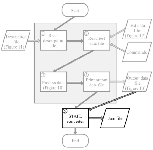
3.4.1 Converting Output Data to STAPL
Standard test and programming language (STAPL) is a high level programming language designed to simplify testing of boundary scan systems. STAPL code is written in ASCII text files called Jam files. Jam files are used together with a Jam STAPL player, which converts the STAPL code to boundary scan instructions at runtime. A Jam STAPL player can be used on an embedded processor for built in testing, which eliminates the need of an external test controller.
This program was developed to verify the output from the Concatenator program on hardware. The hardware used was a demo board developed by SAAB Aerotech AB.
A Jam file with STAPL code can be created from the output data created by the Concatenator program. The response from the STAPL player can then be compared with the expected response in the output data file, to detect any faults.
3 4 Read test data file Read description file Process data (Figure 10) Print output data file End 1 Test data file (Figure 12) Commands Output data file (Figure 13) Description file (Figure 11) STAPL converter 5 2 Start Jam file
Figure 15: Flow chart with STAPL conversion
As seen in Figure 15, the STAPL converter process only use the output data file as input, which contain the necessary information needed to produce STAPL code. The STAPL converter process only converts the output data file to basic STAPL code, which include application of test stimuli and caption of test response of a boundary scan system. The STAPL program run by the STAPL player does not evaluate the response. The evaluation is done by a separate program, described in the next section. 3.4.2 Program to Evaluate Test Response from a Boundary Scan System
A program, developed by SAAB Aerotech AB, named TSTAP-RT was used to test the Concatenator program on hardware. The TSTAP-RT program is the only program used which is not developed by the author of this thesis. The TSTAP-RT program includes a JAM STAPL player and a function to record traffic on the boundary scan port. The recorded traffic is read to extract response from the boundary scan system, to compare with the expected response found in the corresponding output data file (Section 3.3). A log file is created with the result of the comparison. The log file includes the expected data, the read data and the result of the comparison showing which scan cells that are not equivalent.
4
Experiments
Two experiments were conducted to determine how much test data memory requirement can be reduced using the Concatenator program. The first experiment was conducted to gather statistical data using 1000 randomly generated scenarios (Section 4.1. The second experiment was conducted on the ITC´02 SOC test benchmarks (Section 4.2).
4.1
Experiment 1
This section presents the experimental setup and the result of Experiment 1, which was conducted to gather statistical data with randomly generated scenarios. A total amount of 1000 scenarios were generated where each scenario corresponds to a unique configuration of the description and test data files (Section 3.2).
PCB Test Manager / PC
Component 1 Component 2 Component 3
Figure 16: Overview of an embedded system, with an external test manager
Two simplifications are done for the purpose of the experiment. First simplification is that the program is run on a PC instead of an embedded processor on a PCB, as represented by Figure 16, compared to Figure 2 on page 3. The second simplification is that all data files used are text files instead of binary files. By comparing text files representing the stored test data, the expected result is in relative terms the same as when comparing binary files for the same data, and in this study the interesting result is only the relative difference in test data volume.
As seen in Figure 17, the experiment process was divided into three steps. The first step were to generate the files needed, the second step were to run the Concatenator program (Chapter 3) with the files generated, and third step were to evaluate each set of files. The evaluation compared the file size of the description file, test data file and program size to the output data file. Result and conclusion of the experiment are presented in Section 4.1.2.
End The Concatenator Program Start Report size of files Generate Test data file
Generate Description and Commands Done? Database / Save data Output data file Test data file Description file Commands Yes No Generation Program
1
2
3
Figure 17: Program flow for experimentation 4.1.1 Description and Test Data Files
This section presents the process and boundaries concerning the generation of the description and test data files needed to conduct the experiment.
To randomly generate a description file (Section 3.2.1), a few components of one or more types are needed. The content of the description files were generated by randomizing the parameters shown in Table 2. It should be noted that for each component type, the lengths of the boundary scan and instruction registers are required, and these are also taken from random generation as described in Table 2. To conduct the experiment described in this section, a test data file (Section 3.2.2) is needed for every description file. To randomly generate the test data file, some values from the corresponding description file is needed in addition to selecting the number of test patterns per component type, as can be seen in Figure 17. The random values for the description and test data files were generated between the values in Table 2.
Type of value min max
Number of components 2 10
Number of component types 1 #components Boundary scan register length 1 10000 bits Instruction register length 2 20 bits Number of test patterns 1 1000 Table 2: Experimental setup of the description and test data files
and a test data file. The middle column represents the minimum value and the right column represents the maximum value.
The range in which the number of components is chosen is realistic, as can be seen by the following discussion about the minimum and maximum values. The minimum value of two components is chosen since the Concatenator program is not needed in the trivial case of only one component. The maximum number of ten components is chosen since it is big enough to make a good diversity between the results and still small enough to keep the data volume reasonable for experimental purposes; the data volume needed is discussed later in Section 4.1.2. The number of component types is realistic, because a design may consist of completely heterogeneous components or consist of homogeneous components. The boundary scan register length is set to give a good diversity by getting small results as well as bigger ones. Since the instruction register is a small part of the overall test data volume, the instruction register length was chosen to not impact on smaller scenarios. The number of test patterns was chosen low by intention to decrease the data volume needed to conduct the experiment.
4.1.2 Result of Experiment 1
Every pair of description and test data files generated as described in Section 4.1.1 were processed with the Concatenator program. A total of 1000 description and 1000 test data files were generated, which gives a total number of 1000 output data files produced by the Concatenator program.
A large amount of data was generated for this experiment, approximately 37 GiB, since a one or a zero generated in the experiment used one byte instead of one bit. The boundaries set on boundary scan register length and number of test patterns was made to make the time of the experiment reasonable. Below are the real numbers for the data volume for each file type generated in this experiment.
The size of all 1000 description files together made up 307,995 bytes (300 KiB) and the size of all 1000 test data files together made up 11,330,582,604 bytes (10.5 GiB). The size of the description and the test data files are the amount of data that the Concatenator program need in order to create fully defined test patterns (FDTPs), including expected responses.
The size of all 1000 output data files together made up 28,492,295,700 bytes (26.5 GiB). The size of the output data files are the amount of data that would be needed to store all FDTPs, including expected responses.
The Concatenator program itself use 43,520 bytes (42.5 KiB) of memory. To even out the imbalance the size of the Concatenator program is multiplied by 8 to count it in bits instead of bytes. This is done since the description, test data and output data files are counted in bytes as if they were in bits, as discussed in Section 4.1 on simplification.
P
SizeDF +PSizeT DF + (SizeP rogram· #Scenarios)
P
SizeODF
(1) Equation 1 is the equation used to calculate the relative difference in test data volume between using the Concatenator program and storing FDTPs. P
SizeDF is the size of all description files,PSizeT DF
is the size of all test data files andP
SizeODF is the size of all output data files. Since every scenario is
a different test, the size of the Concatenator program (SizeP rogram) have to be multiplied by the number
of scenarios (#Scenarios), which in this case is 1000. With the numbers mentioned inserted in the Equation 1 a result is obtained.
307, 995 + 11, 330, 582, 604 + (43, 520 · 8 · 1000)
Calculation 2 shows that the total amount of memory consumed by the description and test data files were approximately 40% of the output data files consisting of FDTPs. In other words, the data used by the Concatenator program saves approximately 60% memory compared to storing FDTPs.
Test data reduced #Scenarios
>80% 8% >70% 25% >60% 41% >50% 55% >40% 69% >30% 76% >20% 82% >10% 85% >0% 90%
Table 3: Experiment 1 results
Table 3 shows in how many scenarios a certain percentage of test data memory requirements is reduced by the Concatenator program. The left column shows the percentage of reduction of test data memory requirements. The right column shows the percentage of scenarios where the percentage of reduction of test data memory requirements where obtained.
0 100 200 300 400 500 600 700 800 900 1000 -100 -80 -60 -40 -20 0 20 40 60 80 100 T es t d at a re du ce d in p er ce nt Scenario
Figure 18: Sorted graph of Experiment 1 results
Figure 18 shows a sorted graph of the results from Experiment 1. The vertical axis shows the amount of test data reduced in percent and the horizontal axis shows the scenario number.
As seen in Table 3 and in Figure 18, in 55% of the scenarios the Concatenator program decreased the memory needed by more then 50%, and in 76% of the scenarios the program decreased the memory needed by more then 30%, compared to the memory needed to store FDTPs. As seen in Figure 18 the decrease is approximately linear for the first 70% to 75% of the scenarios, at which point the graph starts to decrease at a higher rate towards the horizontal axis.
In 10% of the cases the program increased the memory needed to store test patterns, which can be seen in Figure 18. These cases were small examples where the Concatenator program itself used
more or slightly less memory then the output data, which is seen as a steep fall in the sorted graph, or in the examples of where all components where of different types. The experiment only tested when all devices where used at once and the components of the same type used the same component type specific test patterns. No flexibility were used, for example testing the components one by one or performing different types of tests on different components, which would increase the number of FDTPs and further improve the statistics in favour of the Concatenator program.
4.2
Experiment 2
Experiment 2 was made on the ITC´02 SOC test benchmark. The purpose of this experiment was to see if the Concatenator program were able to reduce test data memory requirements for factory designs.
ITC´02 SOC test benchmarks are a collection of factory designs which purpose is to stimulate research of new methods and tools for modular testing of core-based SOCs and to be able to objectively compare the methods effectiveness and efficiency [17]. The test data for these factory designs is in the order of millions of bits, which can be considered relatively small compared to newer designs with test data in order of billion of bits [2].
The calculations made in this experiment were based on that a component had to have at least one scan chain. If a component had multiple scan chains, all scan chains were added to form one long virtual scan chain. The length of the long virtual scan chain was multiplied by the number of test patterns specified for the component. If two or more components had the same number of pins, scan chains, scan chain lengths and number of test patterns, the components was considered to be of the same type. In three of the SOC designs, test data memory requirements were reduced, which can be seen in Table 4.
SOC design Test data volume Test data volume Test data reduced without Concatenator with Concatenator
f2126 4,914,813 4,868,260 1.0%
p93791 24,515,190 22,666,952 7.5%
q12710 14,129,114 10,400,187 26.4%
Table 4: ITC´02 benchmark results
Leftmost column in Table 4 shows the name of the SOC designs. Second column from the left shows the total test data volume calculated for the SOC design when test data is not reduced using the Concatenator program. Third column shows the test data volume calculated that would be needed to store when the Concatenator program is used. Rightmost column shows the percentage of test data memory requirements reduced by using the Concatenator program.
Since only three out of twelve ITC´02 SOC test benchmark designs have two components of the same type, the statistics does not favour the Concatenator program. However the SOC design q12710 reduced memory requirements with 26.4%, which demonstrates that the proposed concatenator ap-proach is useful for reducing test data memory requirements for well known benchmark designs.
5
Conclusion and Future Work
The target for this thesis was to show a possible solution where increased flexibility and reduced test data memory requirements go hand in hand for embedded testing of systems with multiple components. Many previous studies have focused on reducing test data memory requirements with several different methods. Previous studies have also focused on how to deliver test data to a system for embedded testing, but no study have focused on utilizing the observation of multiple components of the same type in a system to reduce test data requirements and increase flexibility, using deterministic test patterns. A method have been developed to reduce test data memory requirements by storing test patterns specific to every component type (component type specific test patterns, CTSTPs) instead of fully defined test patterns (FDTPs). The method reduces test data memory requirements by reducing the redundancy of test patterns. The method was implemented as the Concatenator program which uses the CTSTPs to create FDTPs when needed. The Concatenator program increase the flexibility by being able to test parts of the system without affecting the rest of the components in the system and without increasing test data memory requirements. Two experiments were conducted to evaluate how much the test data memory requirements is reduced by utilizing the Concatenator program. The first experiment was con-ducted on 1000 randomly generated designs and the second experiment was concon-ducted on the ITC´02 SOC test benchmarks. For the first experiment test data memory requirements were reduced by an average of 60% and in the second experiment test data memory requirements were reduced by up to 26.4%.
For future work, the Concatenator program should be evaluated as part of an embedded system. To make the program work in an embedded system it must be cross-compiled to the CPU platform of the embedded system and possibly there may be some adjustments depending on the design of the embedded system. A further improvement would be to evaluate if it is possible and viable to further reduce memory stored by combining the proposed solution with a compression technique.