Doctoral Thesis in Electronics
Germanium layer transfer and device
fabrication for monolithic 3D
integration
AHMAD ABEDIN
Stockholm, Sweden 2021 www.kth.se ISBN 978-91-7873-834-2 TRITA-EECS-AVL-2021:23 KTH ROYAL INSTITUTE OF TECHNOLOGY AH M AD AB ED IN G erm an iu m l ay er t ra ns fe r a nd d ev ice f ab ric ati on f or m on oli th ic 3 D i nte gra tio n K TH 2 02 1Germanium layer transfer and device
fabrication for monolithic 3D
integration
AHMAD ABEDIN
Doctoral Thesis in Electronics KTH Royal Institute of Technology Stockholm, Sweden 2021
Academic Dissertation which, with due permission of the KTH Royal Institute of Technology, is submitted for public defence for the Degree of Doctor of Philosophy on Friday the 21st May 2021, at 1:00 p.m. in Sal C, Kistagången 16, Stockholm, Sweden.
© Ahmad Abedin
© Mikael Östling, Per-Erik Hellström, Pooria Asadollahi, Konstantinous Garidis, Laura Zurauskaite, Gunnar Malm, Ganesh Jayakumar
ISBN 978-91-7873-834-2 TRITA-EECS-AVL-2021:23
Abstract
Monolithic three-dimensional (M3D) integration, it has been proposed, can overcome the limitations of further circuits’ performance improvement and functionality expansion. The emergence of the internet of things (IoT) is driving the semiconductor industry toward the fabrication of higher-performance circuits with diverse functionality. On the one hand, the scaling of devices is reaching critical dimensions, which makes their further downscaling techno-logically difficult and economically challenging, whereas, on the other hand, the field of electronics is no longer limited only to developing circuits that are meant for data processing. Sensors, processors, actuators, memories, and even power storage units need to be efficiently integrated into a single chip to make IoT work. M3D integration through stacking different layers of devices on each other can potentially improve circuits’ performance by shortening the wiring length and reducing the interconnect delay. Using multiple tiers for device fabrication makes it possible to integrate different materials with superior physical properties. It offers the advantage of fabricating higher-performance devices with multiple functionalities on a single chip. However, high-quality layer transfer and processing temperature budget are the major challenges in M3D integration. This thesis involves an in-depth exploration of the application of germanium (Ge) in monolithic 3D integration.
Ge has been recognized as one of the most promising materials that can replace silicon (Si) as the channel material for p-type field-effect transistors (pFETs) because of its high hole mobility. Ge pFETs can be fabricated at substantially lower temperatures compared to Si devices which makes the former a good candidate for M3D integration. However, the fabrication of high-quality Ge-on-insulator (GOI) layers with superior thickness homogene-ity, low residual doping, and a sufficiently good interface with buried oxide (BOX) has been challenging.
This thesis used low-temperature wafer bonding and etch-back techniques to fabricate the GOI substrate for M3D applications. For this purpose, a unique stack of epitaxial layers was designed and fabricated. The layer stack contains a Ge strain relaxed buffer (SRB) layer, a SiGe layer to be used as an etch stop, and a top Ge layer to be transferred to the handling wafer. The wafers were bonded at room temperature, and the sacrificial wafer was removed through multiple etching steps leaving 20 nm Ge on the insulator with excellent thickness homogeneity over the wafer. Ge pFET devices were fabricated on the GOI substrates and electrically characterized to evaluate the layer quality. Finally, the epitaxial growth of the highly doped SiGe and sub-nm Si cap layers have been investigated as alternatives for improved performance Ge pFETs.
The Ge buffer layer was developed through the two-step deposition tech-nique resulting in defect density of 107cm−3and surface roughness of 0.5 nm.
The fully strained Si0.5Ge0.5 film with high crystal quality was epitaxially
grown at temperatures below 450°C. The layer was sandwiched between the Ge buffer and the top 20 nm Ge layer to be used as an stop in the
etch-back process. A highly selective etching method was developed to remove the 3 µm Ge buffer and 10nm SiGe film without damaging the 20 nm transferring Ge layer.
The Ge pFETs were fabricated at temperatures below 600°C so that they could be compatible with the M3D integration. The back interface of the devices depleted at VBG = 0V , which confirmed the small density of fixed charges at the Ge/BOX interface along with a low level of residual doping in the Ge channel. The Ge pFETs with 70 % yield over the whole wafer showed 60 % higher carrier mobility than Si reference devices.
Low-temperature epitaxial growth of Si passivation layer on Ge was de-veloped in this thesis. For electrical evaluation of the passivation layer, metal-oxide-semiconductor (MOS) capacitors were fabricated and character-ized. The capacitors showed an interface trap density of 3 × 10¹¹
eV−1cm−2, and hysteresis as low as 3 mV at Eox of 4MV/cm corresponding to oxide trap density of 1.5 × 10¹⁰
cm−2. The results indicate that this Si passivation layer substantially improves the gate dielectric by reducing the subthreshold slope of Ge devices while increasing their reliability. The in-situ doped SiGe layer with a dopant concentration of 2.5 × 10¹⁹
cm−3 and resistivity of 3.5 mΩcm was selectively grown on Ge to improve the junction formation.
The methods developed in this thesis are suitable for large-scale M3D integration of Ge pFET devices on the Si platform. The unique Ge layer transfer and etch-back techniques resulted in the fabrication of GOI substrates with high thickness homogeneity, low residual doping, and sufficiently good Ge/BOX interface. The process temperatures for Ge transfer and pFETs fabrication are kept within the range of the M3D budget. Integration of the Si cap for gate dielectric formation and SiGe layers in the source/drain region may increase device performance and reliability.
Keywords: Monolithic, sequential, 3D, silicon, germanium, wafer bonding,
etch back, germanium on insulator, GOI, Ge pFET, low temperature, Si passivation, pn junction
Ahmad Abedin, aabedin@kth.se Department of Electronics
School of Electrical Engineering and Computer Science KTH Royal Institute of Technology, SE-164 40 Kista, Sweden
Sammanfattning
Sakernas internet (eng. Internet of Things, IoT) driver halvledarindustrin mot tillverkning av högprestanda komponenter och kretsar med flertal funk-tionaliteter. Å ena sidan skalas komponenter ned till storlekar där ytterligare nedskalning blir teknologiskt svårt och ekonomiskt utmanande. Å andra si-dan är dagens elektronik inte längre begränsad till kretsar för databehandling. För att sakernas internet ska fungera behöver sensorer, processorer, styrdon, datorminne och även energilagringsenheter integreras på ett effektivt sätt i ge-mensamma chip. Monolitisk 3-dimensionell integration (M3D) baseras på att stapla olika komponentnivåer på varandra. Detta tillvägagångssätt är en av dem mest lovande metoderna för att förbättra kretsarnas prestanda. Prestan-dan förbättras genom att förkorta elektriska ledare och minska fördröjningen i ledarna. Att ha flera komponentnivåer möjliggör integration av komponenter, som kan använda sig av olika material med högkvalitetsegenskaper för olika tillämpningar och funktioner, i ett enda chip. De stora utmaningarna för M3D är högkvalitétsöverföring av skikt och begränsad processtemperatursbudget. Germanium (Ge) anses vara det bästa materialet för att ersätta kisel (Si) som kanalmaterial i p-typs fälteffektstransistorer (pFET) tack vare dess höga hål-mobilitet. Vidare anses germanium lovande för M3D-integration tack germa-niumtransistorernas jämförelsevisa låga processtemperatur mot motsvarande kiseltransistorer. Dock har tillverkning av germanium-på-isolator (eng. germa-nium on insulator, GOI) flera utmaningar: tjockleken på germagerma-niumskiktet måste vara jämnt över skivan, dopningen måste vara låg och gränssnittet mot den begravda oxiden (eng. buried oxide, BOX) måste vara tillräckligt god. I denna avhandling används skivbondning vid låg temperatur och tillbaka-ets för att tillverka GOI-substrat för M3D-tillämpningar. En unik stapling av epi-taxiellt växta skikt har designats och tillverkats för detta ändamål. Skiktstap-lingen innehåller ett relaxerad bufferskikt av germanium, ett etsstoppsskikt av kiselgermanium (SiGe) och ett toppskikt av germanium som i slutändan överförs till en hanteringsskiva. Skivorna direktbondas vid rumstemperatur, och offerskivan togs bort genom flera etssteg som lämnar 20 nm germanium på isolator med utmärkt tjockleksjämnhet över skivan. Germaniumtransistorer tillverkades på GOI-substrat och mättes elektriskt för att utvärdera skiktkva-litén. Epitaxiellt växt av högdopat SiGe och sub-nanometer kiseltäckeskikt (eng. silicon cap layer) utforskades som alternativ för germaniumtransistorer med förbättrad prestanda.
Bufferskikt av germanium togs fram med två-stegs deponeringsteknik vilket gav resultatet att defekttätheten var 107
cm−3 och ytruffighet var 0,5 nm. Töjt Si0,5Ge0,5-skikt med hög kristallkvalité växtes epitaxiellt vid
tempera-turer lägre än 450°C. Skiktet, som infogades mellan bufferskiktet av germa-nium och toppskiktet av 20-nm tjockt germagerma-nium, användes som etsstopp i tillbaka-etsprocessen. En mycket selektiv etsmetod utvecklades för att ta bort den 3-µm tjocka bufferskiktet av germanium och den 10-nm tjocka Si0,5Ge0,5-skiktet utan att skada den 20-nm tjocka germaniumtoppskiktet.
För att tillverkningen av germaniumtransistorerna ska var kompatibla med M3D-integration så tillverkades dem vid en temperatur lägre än 600°C.
Kom-ponentens baksidesgränsnitt (Ge/BOX-gränssnittet) var utarmat vid VBG= 0V , vilket bekräftar att både den fixa laddningstätheten vid gränssnittet och dopningen var lågt. Germaniumtransistorerna hade 70 % avkastning över hela skivan och uppvisade 60 % högre kanalmobilitet än motsvarande komponenter i kisel. In-situ dopat SiGe-skikt med dopningskoncentration på 2.5×1019cm−3
och resistivitet på 3.5 mcm växtes selektivt på germanium för att förbättra käll- och dräneringsövergångsbildningen. Den unika staplingen av grinddie-lektrika Ge/Si/T mSiO/T m2O3/Hf O2/T iN som togs fram i denna
avhand-ling uppvisade en gränssnittsfälltäthet på 3 × 10¹¹
eV−1cm−2 och en hyste-res på låga 3 mV vid ett pålagt elektriskt fält över grinddielektrikastapeln på 4 MV/cm, vilket motsvarar en oxidfälltäthet på 1.5 × 1010cm−2. Dessa
resultat visar att denna grinddielektrikastapel kan potentiellt minska germa-niumtransistorernas undertröskelsving samtidigt som den förbättrar tillförlit-ligheten. Metoderna som har tagits fram i denna avhandling är lämpliga för storskalig M3D-integration av germaniumtransistorer på en kiselplattform. Den unika skiktöverföringmetoden av germanium och tillbaka-ets tekniken resulterade i tillverkningen av GOI-substrat med god tjockleksjämnhet, låg dopning och tillräckligt god Ge/BOX-gränssnitt. Processtemperaturerna för germanium-överföring och transistortillverkning hålls inom ramarna för M3D-integrationens temperaturbudget. Integration av SiGe-skikt i käll/dränerings-områden och kiseltäcket för grinddielektrikumbildning kan öka komponent-prestanda och tillförlitlighet.
Nyckelord:Kisel, germanium, epitaxi, selektiv, pn-övergång, germanium på
isolator, GOI, Ge PFET, bonding, monolitisk, sekventiell, tre dimensionell, 3D, lågtemperarad
Ahmad Abedin, aabedin@kth.se Avdelningen för Elektronik
Skolan för Elektroteknik och Datavetenskap
Contents
Contents i
List of Publications iii
List of Figures vi
List of Tables viii
List of Acronyms ix
1 Introduction 1
1.1 Motivation . . . 1
1.2 Scope, objectives and achievements . . . 3
1.3 Organization of the thesis . . . 6
2 3D Integration 7 2.1 3D Integration . . . 7
3 Epitaxial growth of Ge and SiGe 11 3.1 Epitaxy . . . 11
3.2 ASM Epsilon 2000 Reactor . . . 14
3.3 Epitaxial growth of Germanium SRB on Si(001) . . . 15
3.3.1 Germanium growth using germane . . . 18
3.3.2 Ge growth using digermane . . . 20
3.4 SiGe epitaxial growth on Si and Ge . . . 23
3.4.1 SiGe epitaxial growth using silane-germane . . . 23
3.4.2 SiGe epitaxial growth using disilane-digermane . . . 25
3.4.3 Si0.5Ge0.5 growth on Ge . . . 27
3.5 The full stack growth . . . 28
4 Fabrication of Germanium on insulator 31 4.1 Wafer bonding and layer transfer . . . 32
4.1.1 Direct wafer bonding . . . 32 i
ii CONTENTS
4.2 Removing the sacrificial wafer . . . 34
4.2.1 Smart-Cut and grinding . . . 34
4.2.2 Etch-back . . . 35
4.3 Methods for evaluating wafer bonding . . . 35
4.3.1 Bonding strength measurement . . . 35
4.3.2 Post-bonding process resilience . . . 35
4.3.3 Voids density measurement . . . 36
4.4 GoI fabrication process in this research . . . 37
4.4.1 ALD Oxide Deposition . . . 37
4.4.2 Wafer Bonding . . . 38
4.4.3 Baking . . . 39
4.4.4 Si etching . . . 39
4.4.5 Ge and SiGe etching . . . 40
5 Ge pFET fabrication 43 5.1 Fabrication of Ge pFETs . . . 43
5.2 Fabrication of SoI pFETs . . . 44
5.3 Characterizations of Ge pFETs . . . 45
6 Improvement of Ge transistors performance 49 6.1 Si Cap epitaxial growth on Ge to passivate the surface . . . 49
6.1.1 Si passivation layer deposition . . . 50
6.1.2 Ge MOS capacitor fabrication using Si passivation . . . 52
6.2 Selective epitaxy for source and drain . . . 56
6.2.1 In-situ doped SiGe growth . . . 56
7 Conclusions and outlook 59 7.1 Summary . . . 59
7.2 Outlook . . . 62
Acknowledgements 63
Bibliography 65
List of Publications
This thesis is based on the following papers in peer-reviewed
interna-tional journals and reviewed conference proceedings:
I. ”Epitaxial Growth of Ge Strain Relaxed Buffer on Si with Low Threading
Dislocation Density”
A. Abedin, A. Asadollahi, K. Garidis, P.-E. Hellström, M. Östling ECS Transactions, vol.75, pp.615. (2016)
DOI: 10.1149/07508.0615ecst
II. ”Growth of epitaxial SiGe alloys as etch-stop layers in germanium-on-insulator
fabrication”
A. Abedin*, K. Garidis*, A. Asadollahi, P.-E. Hellström, M. Östling Under review.
III. ”Germanium on Insulator Fabrication for Monolithic 3-D Integration”
A. Abedin, L. Zurauskaite, A. Asadollahi, K. Garidis, G. Jayakumar, B. G.
Malm, P.-E. Hellström, M. Östling
IEEE Journal of the Electron Devices Society, vol.6, pp.588. (2018)
DOI: 10.1109/JEDS.2018.2801335
IV. ”Si-passivated Ge Gate Stacks with Low Interface State and Oxide Trap
Den-sities Using Thulium Silicate”
L. Žurauskait˙e, A. Abedin, P.-E. Hellström, and M. Östling
ECS Transactions, vol.98, pp.387. (2020)
DOI: 10.1149/09805.0387ecst
V. ”Selective epitaxial growth of in situ doped SiGe on bulk Ge substrates for
p+/n junction formation”
K. Garidis, A. Abedin, A. Asadollahi, P.-E. Hellström, M. Östling
Electronics, vol.9, pp.578. (2020)
DOI: 10.3390/electronics9040578 *: Equal Contributions
iv LIST OF PUBLICATIONS
The contribution of Ahmad Abedin to each publication, major ( r r r), partial ( r r), or minor ( r):
Design Fabrication Characterization Analysis Writing
I. r r r r r r r r r r r r r
II. r r r r r r r r r r r r r
III. r r r r r r r r r r r r
IV. r r r r r r r r r
V. r r r r r r r r
The work has also been presented at the following Publications and
international conferences:
VI. ”Semiconductor devices for lasing application and methods of manufacturing such devices
A. Abedin, M. Östling United States Patent Application, US2021/0104871A1,
(2021)
VII. ”Sensitivity of the crystal quality of SiGe layers grown at low temperatures by trisilane and germane”
A. Abedin, M.Moeen, C. Cappetta, M. Östling, H.H. Radamson Thin Solid Films, vol.38, pp.613. (2016)
VIII. ”GOI fabrication for monolithic 3D integration”
A. Abedin, L. Zurauskaite, A. Asadollahi, K. Garidis, G. Jayakumar, B. G.
Malm, P.-E. Hellström, M. Östling
IEEE SOI-3D-Subthreshold Microelectronics Technology Unified Conference (S3S), pp.81-84, Oral Presentation. (2017)
IX. ”IR-Photodetector Fabrication on Suspended Gesn Thin Layers”
A. Abedin, K. Garidis, P.-E. Hellström, M. Ostling ECS Meeting, MA2018-02 1023, Oral Presentation. (2018)
X. ”Integration of highly-strained SiGe materials in 14 nm and beyond nodes FinFET technology”
G Wang, A. Abedin, M Moeen, M Kolahdouz, J Luo, Y Guo, T Chen, H Yin, H.H. Radamson
Solid-State Electronics, vol.103, pp.222-228. (2015)
XI. ”Optimization of SiGe selective epitaxy for source/drain engineering in 22nm node complementary metal-oxide semiconductor (CMOS)”
GL Wang, M Moeen, A. Abedin, M Kolahdouz, J Luo, CL Qin, HL Zhu, H.H. Radamson
v
XII. ”Impact of pattern dependency of SiGe layers grown selectively in source/drain on the performance of 22 nm node pMOSFETs”
G Wang, M Moeen, A. Abedin, Y Xu, J Luo, Y Guo, C Qin, Z Tang, H Yin, H.H. Radamson
Solid-State Electronics, vol.114, pp.43-48. (2015)
XIII. ”Formation of nickel germanides from Ni layers with thickness below 10 nm” L Jablonka, T Kubart, D Primetzhofer, A. Abedin, PE Hellström, M Östling
J. Vac. Sci. Technol., vol.35, 020602. (2017)
XIV. ”Improved designs of Si-based quantum wells and Schottky diodes for IR detection”
M Moeen, M Kolahdouz, A Salemi, A. Abedin, M Östling, HH Radamson
Thin Solid Films, vol.613, pp.19-23. (2016)
XV. ”Scalability Study of Nickel Germanides”
L. Jablonka, T. Kubart, F. Gustavsson, D. Primetzhofer, A. Abedin, P.E. Hellström, Z. Zhang
Paper presented at Materials for Advanced Metallization (MAM), Brussels,
March. (2016)
XVI. ”Effect of strain on Ni-(GeSn)x contact formation to GeSn nanowires” M. Noroozi, M. Moeen, A. Abedin, M.S. Toprak H.H. Radamson
MRS Online Proceedings Library, vol.1707, pp.7-12. (2015)
XVII. ”CVD Growth of GeSnSiC Alloys Using Disilane, Digermane, Tin Tetrachlo-ride and Methylsilane”
M Noroozi, A. Abedin, M Moeen, M Östling, HH Radamson
List of Figures
2.1 Schematic of 3D stacking by using interposer . . . 8
3.1 Schematic of the epitaxial stack for wafer bonding and Ge layer transfer
on insulator . . . 14
3.2 Photo of the quartz chamber of ASM Epsilon 2000 . . . 15
3.3 TDD vs Ge thickness [30]. . . 17
3.4 Ge growth rate versus temperature with germane flow of 400 SCCM at
20 Torr . . . 18
3.5 XRD Omega/2Tetha scan around (004) direction of Ge buffer layer on Si 19
3.6 Etch pit density of Ge SRB revealed by a) Iodine solution and b) Secco
solution . . . 20
3.7 Growth rate of Ge layer on Si substrate at temperatures ranging from
280°C to 600°C with digermane flow of 100 SCCM at 20 Torr . . . 21
3.8 EPD revealed by a) Secco solution and b) Iodine solution. . . 22
3.9 XRD Omega/2Tetha scan around (004) direction of SiGe layers grown
on Si substrates using silane and germane . . . 24
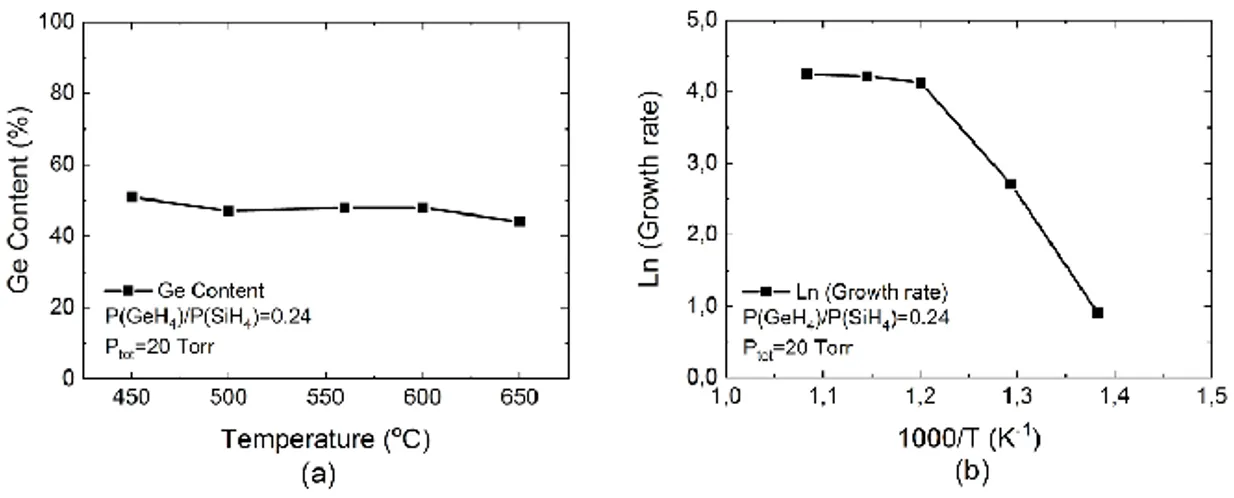
3.10 Ge content and growth rates of the SiGe layers versus temperature at
P (GeH4)/P (SiH4) = 0.24. . . . 24
3.11 Growth rate and Ge contents of SiGe layers versus PPR of germane to
silane . . . 25
3.12 10 µm×10 µm atomic force microscopy (AFM) images of the SiGe
sur-faces grown at P (GeH4)/P (SiH4) = 0.24 in a temperature range of (a)
500ºC, (b) 560ºC, (c) 600ºC, and (d) 650ºC . . . 26
3.13 Ge content and growth rate of SiGe layers as a function of P (Ge2H6)/P (Si2H6),
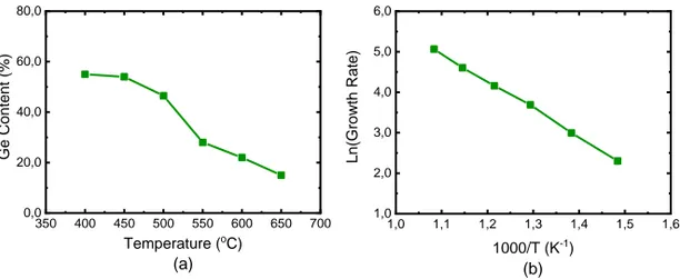
at 450°C and Ptot=20 Torr . . . 26
3.14 The Ge content and growth rate of SiGe layers versus temperature at
P (Ge2H6)/P (Si2H6)=0.067 and Ptot=20 Torr . . . 27
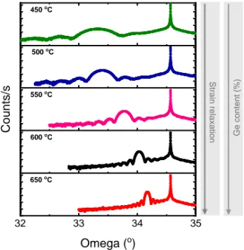
3.15 XRD rocking curve of SiGe layers grown by digermane and disilane at
different temperatures at P (Ge2H6)/P (Si2H6)=0.067 and Ptot=20 Torr. 28
3.16 XRD rocking curve acquired by -2 scan around (004) direction. The
Si0.5Ge0.5 peak position at 34.4° and the thickness fringe to the left
shows that the layer is under tensile strain with a sufficiently flat
inter-face with Ge SRB . . . 29
LIST OF FIGURES vii
3.17 AFM image of Si0.5Ge0.5 layer grown on Ge strain relaxed buffer. The
RMS surface roughness does not change with the deposition of Si0.5Ge0.5
on top of the Ge SRB. . . 30
3.18 AFM surface topology of full-stack containing Si/Ge/SiGe/Ge with RMS
of 0.3 nm . . . 30
4.1 IR image of the bonded SiO2− SiO2 . . . 36
4.2 IR images of bonding process showing bonding wave propagation through
wafer . . . 38
4.3 SEM cross section image of selectively etched Ge/SiGe/Ge/SiGe stack . 40
4.4 Removal of SiGe etch-stop layer and formation of SiO2 during SC-1
etching . . . 41
4.5 a) Optical image of a fabricated GoI substrate, b) Thickness map of a
fabricated GoI wafer with 20 nm Ge on top . . . 42
4.6 AFM image of the surface topography of a fabricated GoI substrate
showing RMS below 0.5 nm . . . 42
5.1 Optical image of six chips fabricated on GoI substrate, b) TEM image
of 0.8 µm pFET device fabricated on GoI substrate . . . 45
5.2 a) ID− VG characteristics of a Ge MOSFET with 0.8 µm gate length,
b) ID− VG behavior under back-bias voltage of -40V to 40V . . . 46
5.3 a) CV curves of Ge/Al2O3 MOS capacitors, b) Carrier mobility in GoI
and SoI pFET devices . . . 47
5.4 Threshold voltage map over wafer . . . 47
6.1 Growth rate of Si versus temperature using silane, disilane, and trisilane 51
6.2 a) Process flow for fabrication of MOS capacitors, b) Schematic
cross-section of gate stack, and c) TEM cross-cross-section image of fabricated gate
stack . . . 52
6.3 (a) CV characteristics of Ge/Si/T mSiO/T m2O3/Hf O2/T iN gate stacks
with Si-cap. (b) Interface state density is 2–4 × 10¹¹eV−1cm−2 at EOT
of 3.75-3.8 nm . . . 53
6.4 Interface state density of Ge/Si/T mSiO/T m2O3/Hf O2/T iN gates as
a function of Si-cap growth time. Average over 10 measuring devices is
displayed. Standard deviation is indicated with error bars . . . 54
6.5 Oxide trap density Nox extracted from CV hysteresis as function of
oxide field Eox. Si-cap devices exhibit more than 20 times lower oxide
trap density than reference GeOx devices . . . 54
6.6 a) AFM image (35 µm × 35 µm) of the p+Si
0.73Ge0.27 film grown
se-lectively on Ge. b) SIMS analysis on 80 nm p+Si
0.73Ge0.27 film grown
selectively on Ge . . . 57
6.7 XRD rocking curve of selectively grown SiGe layer on Ge buffer layer on
List of Tables
1.1 Bulk properties of Si, Ge, and III-V semiconductors . . . 3
5.1 SS comparison with literature . . . 46
List of Acronyms
3D three dimensional
ALD atomic layer deposition
BOX buried oxide
CDE cyclic deposition-etch
CMOS complementary metal oxide semiconductor
CV capacitance-voltage
CVD chemical vapor deposition
CVE chemical vapor etch
DCS Dichlorosilane
FET field effect transistor
FDSOI fully depleted silicon on insulator
IV current-voltage
LPCVD low pressure chemical vapor deposition
M3D monolithic three dimensional (integration)
MOS metal oxide semiconductor
MOSFET metal oxide semiconductor field effect transistor
NW nanowire
PECVD plasma enhanced chemical vapor deposition
PVD physical vapor deposition
RIE reactive ion etching
RPCVD reduced pressure chemical vapor deposition
RTA rapid thermal anneal
SEG selective epitaxial growth
SEM scanning electron microscope
SIMS secondary ion mass spectroscopy
SOI silicon on insulator
SS subthreshold slope
STL sidewall transfer lithography
TEM transmission electron microscope
TMAH tetra-methyl-ammonium-hydroxide
Chapter 1
Introduction
1.1
Motivation
Electronic circuits dramatically changed in the 1960s as they moved from being conventional discrete devices to be the integrated components on a single chip [1]. Integrated electronics improved the reliability and performance of these circuits even as they reduced the cost of design and fabrication. Since then, the dimensions of MOS devices have been continuously downscaled allowing for a larger number of devices per area and faster switching speed [2]. Such downscaling has increased the performance of these circuits while reducing fabrication costs. Today, however, the field of electronics is facing new challenges.
On the one hand, the scaling of devices is reaching critical dimensions in the order of several atoms. This makes further downscaling technologically difficult and economically not beneficial [3]. In turn, it makes 3D integration involving stacking different layers of devices on each other, one of the most promising methods for improving circuits’ performance while keeping the costs down and avoiding atomic-scale challenges [4]. On the other hand, today, the field of electronics is no longer limited to circuits with only data processing applications [4]. IoT systems are emerging, and they require multiple functionalities on a single chip. Sensors, processors, actuators, memories, and even power storage units need to be efficiently integrated to make IoT work [5]. Stacking different device layers on top of each other is one of the most promising methods to overcome these challenges.
One of the advantages of 3D integration over 2D integration is the possibility of using different materials as the active layer in the circuit. As pFETs (p-type field effect transistors) and nFETs (n-type field effect transistors) are fabricated
2 CHAPTER 1. INTRODUCTION
on different tiers, they can be processed sequentially using different materials and techniques [4]. However, their sequential processing imposes a temperature limit on the process. The processing of the top-tier devices must be tuned such that it minimizes the damages to the bottom tier and maintains the performance of already fabricated devices in the first layer. Therefore, it is important to choose the right material for the top tier which would have high carrier mobility and low processing temperature and be compatible with Si CMOS technology.
Ge as top tier material
Ge is one of the most promising candidates for 3D integration with Si devices. It has high carrier mobility compared to Si and a natural lower processing temperature. The first transistor invented in 1947 at the Bell Telephone Laboratories was made on a Ge block [6]. However, it was replaced by Si in the 1960s due to the many advantages of Si. High purity Si substrates were easier to produce, and Si could stand much higher temperatures. However, the main reason for replacing Ge with Si was the high stability of silicon dioxide. Ge oxide is water-soluble, which made it quite difficult to process. The formation of multiple sub oxides GexOy degraded the surface passivation capabilities and limited its application as a high K dielectric [7]. SiO2, on the other hand, could be thermally grown in a well-controlled manner and used as an efficient passivation layer for transistor fabrication. The high stability of SiO2 made Si the best material for the mass production of transistors, and that has remained so until today [8].
Recently, however, advanced gate dielectric materials have been developed using the atomic layer deposition technique. Therefore, there has been growing interest in Ge as the material for future electronics [4]. Ge has a much smaller effective mass in the heave hole (mhh) and light hole (mlh) bands compared to Si. This small effective mass leads to its potentially higher carrier mobility compared to Si. A comparison of the bulk mobilities of Si, Ge, and III-V semiconductor materials is presented in table 1. It can be seen from table 1 that Ge has considerably higher hole mobility than the other semiconductors, which enables enhancing the drive currents in Ge pFETs. By just considering the mobility values, III-V for NMOS (n-type metal oxide semiconductor) and Ge for PMOS (p-type metal oxide semiconductor) seems to be the best combination. However, the fabrication of nanoscale III-V transistors on Si platform suffers from cost and process compatibility issues.
Besides the higher carrier mobility advantage of Ge, its low-temperature process-ing also makes it a good candidate for M3D integration. Since Ge is a group IV ma-terial, it is compatible with Si technology and does not add any cross-contamination issues. SiGe has been already used in CMOS fabrication. Therefore, integration of Ge as the active material in the existing CMOS technology will be straightforward.
1.2. SCOPE, OBJECTIVES AND ACHIEVEMENTS 3
Material/property Si Ge GaAs InAs InSb
Electron Mobility cm2/(V.s)) 1600 3900 9200 40000 77000
Hole Mobility cm2/(V.s)) 430 1900 400 500 850
Bandgap (eV) 1.12 0.66 1.424 0.36 0.17
Dielectric Constant 11.8 16 12.4 14.8 17.7
Table 1.1: Bulk properties of Si, Ge, and III-V semiconductors
Although using Ge has many advantages for CMOS applications, its 4% lattice mismatch with Si makes it difficult to grow high-quality layers directly on Si. The low bandgap of Ge and its higher dielectric constant causes the short channel effect and high leakage current, which can be improved by using GoI substrates instead of bulk Ge. Electronic and photonic devices based on GoI have been shown to be promising solutions for addressing the current difficulties that the electronics industry is facing. However, the fabrication of large-scale thin GoI (top Ge layer <40 nm) wafers with high thickness homogeneity, low defect density, low doping level, and good interface quality is challenging.
1.2
Scope, objectives and achievements
This research aims to develop and investigate new methods to use Ge in the sequen-tial fabrication of 3D integrated electronics. Fabrication of high-quality ultra-thin GoI substrate with high thickness homogeneity has been investigated in this re-search to expand the applications of Ge in M3D integrated circuits fabrication.
Five main objectives were defined for this thesis to address the difficulties in Ge M3D integration. These objectives constitute the main contribution of the thesis. The research objectives and the achievements are the following:
Development of Ge SRB to be used as a virtual substrate for trans-ferring the top tier device layer on an insulator.Since the Ge layer is required
to be single crystalline material with a sufficiently low density of defects, a strain relaxed Ge layer is desired to be epitaxially grown on Si substrate. The layer should have ultra-smooth surface morphology (root mean square (RMS) < 1 nm) to be bondable to the insulator layer. The threading dislocation density should be kept low for better device yield over the wafer. By using the two-step method, Ge layers
with threading dislocation density (TDD) of 107 cm−3 were epitaxially grown on
Si substrates. Hydrogen thermal annealing was carried out to reduce the surface roughness to values below 1 nm. These contributions are discussed in section 3.3 and paper I (listed earlier in the “List of Publications”).
4 CHAPTER 1. INTRODUCTION
Development of epitaxial growth of fully strained SiGe thin films to be used as etch-stop layers in GoI fabrication process. To transfer the
ultra-thin Ge layer to another wafer coated with an insulating material, an etch-stop layer is required, which does not add any defects or roughness to the surface. For this purpose, SiGe layers were epitaxially grown at different temperatures using silane-germane and disilane-digermane gas chemistries. As a result, a SiGe layer containing 50% Ge atoms was developed at temperatures below 450°C, which was fully strained toward Ge SRB. A highly selective etching process was developed that successfully removed microns of Ge while keeping the 20 nm transferring layer intact. The contributions are discussed in section 3.4 and paper II (listed earlier in the “List of Publications”).
Wafer bonding and etch-back process development to be adopted for the fabrication of ultra-thin Ge on the Insulator. A wafer bonding technique
and an etch-back process were required for transferring the desired Ge layer to another wafer that would be compatible with 3D integration. This process was developed through room temperature wafer bonding, a combination of wet and dry etching of Si wafer, Ge buffer, and SiGe etch-stop layers. The fabricated GoI wafers exhibited 5% thickness inhomogeneity over the whole wafer. To our knowledge, such a high thickness homogeneity was not reported in any other studies. Since no ion implantation was performed for the GoI fabrication, the residual dopant
concentration was in the range of 1016cm−3 which is much lower than the range
referred to in the previous reports on GoI fabrication methods. The contributions are discussed in section 4.4 and paper III (listed earlier in the “List of Publications”).
Ge pFETs’ fabrication process compatible with M3D. The advantages of
using Ge as the top-tier device material has been discussed in section 1.1. However, the pFETs’ fabrication process needs to be carried out at temperatures below 600°C for it to be compatible with M3D integration. In the course of this research, Ge pFETs’ fabrication process was developed on GoI wafers. The maximum processing temperature and duration were 600°C for 60 s respectively during the dopant-activation step. Therefore, this process is fully compatible with M3D integration. The 70% yield over the wafer indicated that the wafer bonding and the etch-back process are sufficiently reliable for large-scale Ge device fabrication. Ge devices have shown 60% higher carrier mobility compared to the reference Si devices. The back-gate bias characterizations showed that the Ge/Box interface is depleted at 0 V which can be interpreted as a low-charge density at the interface and low level of residual dopants in the Ge channel. The SS of 170 mV/dec was extracted from the
ID− VG characteristics of the GoI devices. This SS value was in the same range as
it was in the other studies. The contributions are discussed in chapter 5 and paper III (listed earlier in the “List of Publications”).
1.2. SCOPE, OBJECTIVES AND ACHIEVEMENTS 5
Development of Si passivation for improvements in Ge devices. Ge
MOS field-effect transistors (MOSFETs) suffer from high oxide trap density (Nox)
and interface trap density (Dit) at the interface of the Ge layer and the high-K
stack, which increases the SS significantly and degrades the reliability. In this thesis, the epitaxial growth of an ultra-thin Si cap layer on Ge is developed to passivate the surface and minimize the high-K dielectric degradation. The sub-nm Si cap layer is deposited at temperatures as low as 400°C and reduced pressure by using disilane precursor. The low-temperature deposition reduces the chance of strain relaxation and minimizes the interdiffusion of Si and Ge atoms at the Si/Ge interface. MOS capacitor devices were fabricated and characterized by the collab-orators to electrically evaluate the Si passivation layer. The capacitors fabricated on Si passivated Ge layers shown similar behavior as the capacitors fabricated di-rectly on Si substrate. The characterization results shown interface trap density of
3×10¹¹eV−1cm−2, and hysteresis as low as 3 mV at Eoxof 4 MV/cm corresponding
to oxide trap density of 1.5×1010cm−2. The results indicate that this Si passivation
layer substantially improves the gate dielectric quality and potentially reduces the SS of Ge devices while increasing their reliability. The contributions are discussed in section 6.1 and paper IV (listed earlier in the “List of Publications”).
Improving the junction formation in Ge devices. High contact resistance
is one of the major issues that Ge devices face. The low doping concentration levels in ion-implanted Ge and high-temperature annealing requirements make it difficult to drive a high current through Ge transistors. To address this issue, we have investigated the selective epitaxial growth (SEG) of highly doped SiGe layers in source and drain areas. The in-situ doped SiGe layer with a dopant concentration
of 2.5 × 1019cm−3 and resistivity of 3.5 mΩcm was selectively grown on Ge to
improve junction formation. PN diodes are fabricated on the heterojunction and characterized to evaluate the layers. The contributions are discussed in section 6.2 and paper V (listed earlier in the “List of Publications”).
The following research milestones were achieved while carrying out the work presented in this thesis:
• Process design for fabrication of ultra-thin GoI substrate with superior thick-ness homogeneity.
• Epitaxial growth of Ge SRB layer on Si substrate with low TDD and smooth surface.
• Epitaxial growth of fully strained SiGe layers on Ge at low temperatures. • Room temperature wafer bonding and low-temperature post-bonding baking
to fabricate large-scale GoI substrates within the M3D integration tempera-ture budget.
• Highly selective etching method to remove the microns of Ge without affecting the 20 nm transferring Ge layer.
6 CHAPTER 1. INTRODUCTION
• Fabrication of Ge pFETs at temperatures below 600°C with excellent electri-cal characteristics.
• Development of highly reliable Si passivation layer on Ge resulting in a gate
stack with low Ditand oxide trap density.
• SEG of highly doped SiGe on Ge to form junctions in the source and drain regions.
1.3
Organization of the thesis
This thesis comprises seven chapters as follows:
Chapter 1 presents the motivations behind this research. This chapter includes
the scope, aims, and achievements of this research.
Chapter 2 briefly introduces 3D integration applications and methods and
state-of-the-art circuits and devices.
Chapter 3 summarizes the theoretical principles behind the epitaxial growth
of Si-Ge alloys. The initial results of the epitaxial growth of Ge SRB and SiGe layers too have been presented in this chapter.
Chapter 4 details the single-crystal Ge layer transfer and GoI substrate
fabri-cation process during this research.
Chapter 5 provides an analysis of the fabrication process and the electrical
characterization results of Ge pFET devices fabricated on our GoI wafers.
Chapter 6 focuses on the optimization of Ge devices through Si surface
passi-vation for better high-K material development, and SEG of highly doped SiGe to improve junction formation in the source/drain region.
Chapter 7 the concluding chapter, provides the highlights of this research and
Chapter 2
3D Integration
This chapter briefly introduces 3D integration and state of the art. 3D integration that is now seen as the solution for IoT device fabrication along with a discussion on the different methods for achieving 3D integrated circuits.
2.1
3D Integration
3D integration, as an idea, got introduced in 1964 by Texas Instruments [4]. Fujitsu demonstrated the first 3D CMOS integrated circuit in 1983, which included the stack of one type of transistor above a transistor of the opposite type [4]. However, the fabrication costs per transistor in 3D integration were much higher than in 2D miniaturization, which limited the industrial application of this method. The increase in the required investments for further 2D scaling, the need for shorter interconnects to get benefit from high-performance devices, and the introduction of new materials and technologies made 3D integrated circuits interesting again. Nowadays, applications of 3D integration technology are expanding rapidly. Some of the driving forces for 3D integrations are miniaturization, cost reduction, multi-functionality, and performance enhancement. There are three major categories of 3D stacking technologies today: using interposer, parallel through-Si-vias (TSV) integration, and monolithic sequential integration.
3D stacking with interposer (2.5D integration)
In this method, circuits are fabricated separately and attached to an interposer. The interposer provides interconnections between the circuits and acts as a supporting platform for multi-chip solutions. This technique permits high metal thickness but
8 CHAPTER 2. 3D INTEGRATION
not high density. Therefore, it is most useful for biosensing and photonic appli-cations with low-density interconnections [9]. Typical thicknesses of interposers are in the 100 µm range with TSV width and space of 1–10 µm. Bumps used for connecting different chips are usually in the range of 40 µm, while the bumps for joining the interposer are typically in 150+ µm pitch. Figure 2.1 illustrates three chips stacked on each other of which two of the chips include TSVs. These two top chips are stacked face-to-face (F2F), while the bottom chips are joined face-to-back (F2B) [10].
Figure 2.1: Schematic of 3D stacking by using interposer
3D parallel integration TSVs
In this technique, circuits are fabricated on two wafers separately and planarized. Two mirror-polished wafers with metal pads (usually Cu) are aligned and put into contact with each other. Adhesive forces are usually applied at room tempera-ture to form the necessary bonding. The circuits´ electrical contacts are reached through TSVs from the backside of the wafer. This technique becomes more and more attractive because of its advantages such as no temperature limitations for separate circuits’ processing and higher interconnection density compared to the flip-chip technology [10]. Nowadays, most image sensors are fabricated using this method [11]. Sony presented the first 3-layer stacked state-of-the-art CMOS image sensor at the IEEE International Electron Devices Meeting (IEDM) 2017. This chip includes pixel, memory, and image signal processor dies mounted on top of each other. They have shown that integrating memory with the logic enhanced the reading speed of the chip from 30 to 120 frame per second [12]. The intercon-nections pitch in this technique is 1 µm, which is limited by the wafer alignment accuracy. The misalignment between the top and the bottom pads would increase the contact resistivity and reduce the yield. Some other challenges in this technique are choosing the right materials, surface preparation, bonding strength, and metal atoms diffusion.
2.1. 3D INTEGRATION 9
Sequential M3D
The first 2D integrated circuit introduced by Jack Kilby in 1958 was not monolithic [1]. The components were fabricated on a single piece of semiconductor, but the interconnections were made using hand soldering. In 1961, the first monolithic 2D circuit was presented by Robert Noyce in which both components and interconnec-tions were monolithically integrated on a single piece of semiconductor [13]. The same story has got repeated in the case of 3D integration 50 years hence. The first 3D integrated circuits are separately made circuits, which are connected to each other by wires or TSVs. However, for higher interconnect density, M3D is required. Sequential M3D is an ideal alternative to parallel stacking to increase the density of interconnections and reach few tens of nanometer pitches. In this method, the tiers are fabricated on top of each other in a sequential manner. Thus, the M3D process has the following five main steps:
• Step 1: The first-tier transistors are fabricated on a Si or SoI substrate followed by metallization and contact formation. The first-tier transistors are fabricated on a Si or SoI substrate followed by metallization and contact formation.
• Step 2: The surface is passivated with an insulator material and planarized using chemical mechanical polishing (CMP).
• Step 3: The wafer is bonded to another wafer for active layer transfer. The second wafer is called a sacrificial wafer. It contains the active layer of the second-tier devices.
• Step 4: The active layer is transferred to the insulating material, and the sacrificial wafer is removed.
• Step 5: The second-tier devices are fabricated directly on top of the first-tier devices, and the circuits are interconnected through conventional photolithog-raphy, etching, and metallization.
This process can be continued with several tiers to add higher devices and functionalities to the 3D integrated chip. Since the same alignment marks can be used for the fabrication of different tiers, lithography alignment precisions of a few nm can be achieved. This high alignment accuracy range enables via densities of more than 100 million/mm2 between different tiers. Since the nFETs and pFETs are fabricated separately, it is possible to use several materials and technologies for the transistors’ performance improvements. For instance, channel materials with higher carrier mobility can be used. Substrate orientation and strain level
10 CHAPTER 2. 3D INTEGRATION
can be different, and various technologies such as FinFET, fully depleted silicon-on-insulator (FDSoI), and nanowire transistors can be built on top of each other. However, some benefits do not come without attendant troubles.
The major limitation of sequential 3D integration is the thermal budget of top tiers’ fabrication. A reasonable max process temperature is determined to be around 500°C for 2 hours, which can be increased to 600°C if the duration would be lesser [14]. Thermal stability of silicide and metal gate function are the bottlenecks for high-temperature processing. Therefore, the top-tier materials and processing must be chosen correctly to prevent degradation of the bottom-tier transistors while achieving excellent top-tier transistor performance. Ge and III-V materials are con-sidered good candidates for top-tier transistors channel material because of their considerably higher carrier mobility and lower processing temperature compared to Si [15]. Stacking InGaAs nFET on top of SiGeOI pFET is one of the best examples of high-performance CMOS circuits made through sequential 3D integration [16], [17]. In the case of using Si as the active layer of the top-tier transistors, new techniques such as laser annealing and solid phase epitaxy are required to keep the bottom tier circuits intact [18], [19].
One of the main challenges in sequential 3D integration is the formation of
top-tier channel material. This layer can be achieved by either polycrystalline
material deposition followed by recrystallization or direct wafer bonding and layer transfer. Layer transfer is usually more complicated compared to polycrystalline material deposition, and more processing steps are required. However, it has many advantages arising from the single crystallinity of the layer, which compensates for the difficulties.
In this thesis, Ge is investigated as one of the most promising candidates for M3D integration on the Si platform. The reason for choosing Ge is the higher carrier mobility compared to alternative semiconductor materials and the ability to process Ge devices at low temperatures. To monolithically integrate Ge on the already processed Si devices, a unique stack of Si/Ge/SiGe/Ge was epitaxially grown on Si substrates. Low-temperature processes are developed for wafer bonding, etch-back, Ge pFET fabrication, and device performance enhancements. The process steps are discussed in detail in the next chapters.
Chapter 3
Epitaxial growth of Ge and SiGe
Epitaxial growth of Ge, SiGe, and Si layers is discussed in this chapter. The basic concepts behind epitaxial growth are explained with a focus on growth kinetics, and strain relaxation. The layers developed at this step have been used later for the fabrication of Ge on the insulator layer and for Ge pFETs’ performance improve-ments.
3.1
Epitaxy
The term epitaxy has a Greek root meaning “arranged on”. It was first used by Royer in 1928. It is defined as oriented growth of a single crystal material arranged upon a single crystal substrate. The mechanism behind epitaxy is that of lowering the internal energy of the system by aligning the atoms of the guest crystal following the same crystal orientations as the host crystal. This enables the growth of ex-ceptionally high-quality crystalline materials without increasing the defect density of the substrate.
Epitaxial growth can be either homoepitaxy if the layer and substrate are the same materials, or hetroepitaxy if the substrate and layer are different materials. Many different techniques have been developed for the epitaxial growth of high-quality materials. Among them, the two most used methods for the epitaxial growth of group IV semiconductors are molecular beam epitaxy (MBE) and chemical vapor deposition (CVD). In MBE, the source materials are evaporated from heated cells and collimated in a single beam before directing them toward the surface of the substrate. MBE is a flexible method as, in it, the growth parameters can be changed independently. However, this flexibility comes with other limitations such as a low deposition rate which limits MBE’s application mainly to research purposes. CVD has a much higher throughput compared to MBE, which makes it a popular method for the deposition of a wide range of materials. Currently, it is the most used method
12 CHAPTER 3. EPITAXIAL GROWTH OF GE AND SIGE
for epitaxial growth of semiconductor materials because it affords high thickness and composition homogeneity, and reproducibility concerning the wafer and over time (wafer-to-wafer).
In CVD, preheated substrates are exposed to precursors in the gas phase, and the desired layers are grown. Since the reactants are chemically stable at room temperature, the deposition is limited only to the heated zones. Chemical reactions determine the composition and the deposition rates of the layers. Therefore, many parameters such as pressure, temperature, and precursor flow control the layer quality, deposition rate, and compositions of CVD. There are many different CVD processes such as low-pressure CVD (LPCVD), reduced pressure CVD (RPCVD), plasma-enhanced CVD (PECVD), and ultra-high vacuum CVD (UHCVD).
There are two types of reactions that happen during epitaxial growth in a CVD process: gas-phase (homogeneous) and solid-surface (heterogeneous) reactions. A homogeneous reaction happens when the source gasses decompose before reaching the surface and produce solid products. The synthesized particles land on the sub-strate’s surface after the reaction causing defects and poor uniformity. Therefore, in our CVD process, gas-phase reactions were not desirable. In a heterogeneous reaction, the reactant molecules are diffused to the surface where the reaction hap-pens, and the desired materials are grown epitaxially. In our process, the layers grown in heterogeneous reactions were more uniform and desired.
The following are two main parameters in a simplified CVD process mechanism: • Reactant molecules’ diffusion to the surface in the gas phase.
J1= D
dC dx ≈
Dg
δ (Cg− Cs) = hg(Cg− Cs) (3.1)
Where J1 is the flux of the reactant molecules in gas phase to the substrate
surface, D is the diffusion constant of the reactant gasses, Cg is the concentration
of reactant molecules in the bulk gas, Csis the concentration of reactant molecules
on the surface, δ is the thickness of the boundary layer, and hgis the mass transfer
coefficient.
• Adsorption of the reactant molecules on the surface.
J2= KsCs (3.2)
Where J2is the flux of reactant molecules in the reaction site, Ksis the reaction
rate constant, Csis the concentration of reactants on the surface.
The by-products need to be desorbed from the surface after the reaction and diffused from the surface to the gas-phase to be removed from the reactor. When
3.1. EPITAXY 13
the deposition rate is limited by the surface reaction, these two steps can be ignored, and a steady-state can be achieved. In the steady-state, the two fluxes are equal to the steady-state flux, which can be calculated as shown below:
JSS = kTCg (3.3)
Where kT is the overall rate constant defined by the mass transfer coefficient
(hg) and the surface reaction rate constant (ks):
kT =
hgkS
hg+ kS
(3.4)
At high temperatures ks> hgwhich results in kT≈ hgwhich means the reaction
is in diffusion controlled regime. In the case of low-temperature processing, however,
ks< hg which corresponds to kT ≈ Ks and the reaction will be in surface reaction
controlled regime. This temperature effect is mainly due to exponential variation of surface reaction constant with temperature versus small variation of diffusivity
by temperature (αT3/2).
Therefore, the growth rate is highly temperature dependent in the reaction controlled regime. The deposition rate of a film with N number of atoms and the overall deposition rate can be calculated from 3.5 and 3.6.
G = JSS N (3.5) Gtot= kT N( 1 KT)Pg (3.6)
where Pg is the partial pressure of the reactant gasses, and K is the Boltzmann
constant.
In this thesis, two different layers are epitaxially grown on Si substrate to be used for fabrication of ultra-thin Ge on insulator layer for 3D integration applica-tion. The first layer consists of a strain-relaxed Ge layer grown directly on the Si substrate. The second layer is a SiGe layer that is epitaxially grown on the Ge layer to be used as an etch-stop layer in the GoI fabrication process. There are two important parameters for the transferring layer to achieve a high process yield and sufficiently good quality material for device fabrication. These parameters are low surface roughness (below 1 nm) and low defect density. The epitaxial stack shown in figure 3.1 was designed to achieve high crystal quality with a defect density of
1 × 1017cm−2 and surface roughness below 1 nm.
This chapter details reduced pressure chemical vapor deposition (RPCVD) of Ge buffer, SiGe etch-stop, doped SiGe contact, and Si cap layers. The
epitax-14 CHAPTER 3. EPITAXIAL GROWTH OF GE AND SIGE
ial growth and effects of parameters such as precursors, deposition temperature, thermal annealing, and thickness have also been discussed in detail.
Figure 3.1: Schematic of the epitaxial stack for wafer bonding and Ge layer transfer on
insulator
3.2
ASM Epsilon 2000 Reactor
ASM Epsilon 2000 is a single wafer RPCVD tool equipped with a load-lock and wafer handling unit. The wafer handling unit and the load-locks are purged with nitrogen (N) to minimize surface oxidation and oxygen contamination. The wafer handling uses a Bernoulli wand to transfer wafers from the loading cassette to the processing chamber and from the processing chamber to the unloading cassette. In the process chamber, which is made of quartz, the wafers are placed on a silicon carbide coated susceptor which is heated by using lamps from the top and the bottom. The process chamber of Epsilon is shown in figure 3.2.
The gas module handles two Ge sources, four Si sources, two dopant gasses, one
tin source, HCl, H2, andN2. Silane, disilane, trisilane, and dichlorosilane (DCS)
are the Si sources. Germane and digermane are the Ge sources. P-type and N-type
doping are obtained by diborane and phosphine gasses respectively. H2andN2 are
used as charrier gasses. HCl can be used in high flow for cleaning the reactor or in low flow for SEG. Each gas line can go to the vent or the reactor separately, which offers the option of depositing different materials on top of each other in a single epitaxial growth step. The processes can be carried out either at reduced pressures (10–100 Torr) or at atmospheric pressure.
The susceptor is heated through radiation from Tungsten-halogen lamps. There-fore, the susceptor’s temperature is much higher than the rest of the reactor, and a major part of the reaction happens on the wafer. The temperature is measured through five thermocouples placed in the center, sides, front, and end of the suscep-tor area. The thermocouples are connected to temperature-controlling units which adjust the power supplied to the lamps separately for each of them so that they
3.3. EPITAXIAL GROWTH OF GERMANIUM SRB ON SI(001) 15
can reach the temperature set-point homogenously over the wafer. The process temperature can be precisely controlled between 200℃ and 1,200℃.
Figure 3.2: Photo of the quartz chamber of ASM Epsilon 2000
3.3
Epitaxial growth of Germanium SRB on Si(001)
Heteroepitaxial growth can be classified into three distinct modes which have been detailed in the following paragraph. Growth mode mainly depends on two param-eters, i.e., the lattice mismatch between the growing layer and the substrate and
the balance between the free energy of substrate (σs), layer (σL), and the interface
(σi).
The Frank-Van der Merwe growth mode is the case where the free energy of the substrate is higher than the free energy of the layer and the interface. In this mode, the single crystalline film is grown layer-by-layer on top of the substrate. It is also called 2D growth. The Volmer-Weber growth mode is the one where the free energy of the substrate surface is lower than the layer and the interface. Therefore, the adatoms bond to themselves to have the minimum free energy and form 3D islands that cause rough surfaces. The third growth mode is the Stranski-Krastanov (SK) mode. It is a combination of both 2D and 3D growth modes. In this case, the growth begins with the 2D layer formation and continues with 3D growth and formation of islands due to gradual strain accumulation. SK is the main mode for epitaxial growth of Ge layers on Si substrate [20].
Ge, with a lattice constant of 5.530 Å, has a 4% lattice mismatch with Si hav-ing a lattice constant of 5.530 Å. This lattice mismatch makes it difficult to grow smooth single-crystalline layers having less defect density. The critical thickness of Ge on Si is reported to be less than 9 atomic monolayers and depends on the growth conditions. The first few monolayers of Ge on Si will be compressively strained since the layer’s in-plane crystal lattice matches the substrate. However, by growing Ge
16 CHAPTER 3. EPITAXIAL GROWTH OF GE AND SIGE
layers thicker than the critical thickness, the layer loses the strain gradually through defect formation. By continuing the growth, these defects penetrate through the film and generate threading dislocations that degrade the crystalline quality and electrical properties of the material. Besides the defect formations, the 3D island growth of Ge on Si increases the surface roughness that degrades device perfor-mance. Several different techniques have been proposed and developed to improve the surface roughness and lower the defect density. These techniques include graded SiGe buffer layers [21, 22, 23], two-step growth (low temperature and high temper-ature), and thermal annealing.
Two step Ge epitaxial growth on Si
The two-step method was proposed in 1998 by Colace et al. [24] and further
developed by Hartman et al. and Luan et al. [25, 26, 27]. In this method, first, a Ge seed layer is deposited at low temperature (LT) (below 400°C) and then a second Ge layer is grown on the seed layer at higher temperatures (HT) (above 550°C).
In the low temperature step, 50–100 nm Ge layer is grown on Si surface to gradually release the 4% misfit stress through misfit dislocations formation. The surface mobility of Ge atoms is substantially low at temperatures below 400°C. This lower atom mobility leads to 2D growth morphology instead of 3D and lowers surface roughness compared to high temperature growth [28]. The seed layers grown
at this step have a high density of threading dislocations in the orders of 1012cm−2.
Therefore, they are not suitable for electronics applications at this stage.
In the second step, Ge layers are grown at temperatures above 600°C to achieve higher crystal quality and faster deposition rates. By growing thicker Ge layers, threading dislocations collide and eliminate each other. As a result, growing thicker layers reduces the level of TDD [29]. However, the thickness cannot be increased more than five microns as the Ge layer has a slight tensile strain and bends the Si wafer. Therefore, post-cycle thermal annealing has been proposed to improve the crystal quality and surface roughness [29]. During cycle thermal annealing, the temperature is increased up to 900°C and reduced to 100°C several times. Yamamoto et al. [29] have shown that by choosing the right temperatures and
thickness, it is possible to reduce defect densities to 7 × 105cm−2while keeping the
surface roughness below 1 nm (figure 3.3). However, thicknesses as high as 4.5 µm are required.
In this thesis research, a two-step process followed by thermal annealing was used for epitaxial growth of the Ge buffer layer with sufficiently high crystal quality. Two commercially available gas sources, germane and digermane, were used for the
3.3. EPITAXIAL GROWTH OF GERMANIUM SRB ON SI(001) 17
directly after growth to reduce the defect density to 107cm−2. The results of
the growth conditions and material characterizations have been presented in this chapter.
Figure 3.3: TDD vs Ge thickness [30].
Pre-Epitaxy treatment
The surface of the wafers must be perfect and without any contaminations to achieve high-quality epitaxial growth. Basically, an epitaxy-ready surface needs to be free from oxide films, contaminations, and etched-surface damages. The best choice for surface preparation is performing both ex-situ and in-situ cleanings. Different processes for wafer cleaning have been presented in [30]. One of the most common
choices for ex-situ cleaning is treatment in a “Piranha” (H2SO4: H2O2) solution to
oxidize the surface and remove organic contaminations. The process is followed by hydrofluoric acid (HF) treatment to remove the native oxide and particles on the surface. The in-situ surface treatment can be performed at different temperatures and gas ambient conditions. Using hydrogen at elevated temperatures is the most common in situ treatment for group IV materials growth. This step can be skipped if cluster tools with in situ wet cleaning stations are being used [31].
For this research, the layers were grown on 100 mm Si wafers that were sub-merged in a “Piranha” bath for 15 min, rinsed in di-water, and dipped in an HF solution before loading to the nitrogen purged load-lock. Substrates were in-situ hy-drogen baked at 1,050℃ for 10 seconds. This prebaking step was enough to remove all oxygen and carbon contaminations that remained on the surface. In the case of Ge wafers and pre-processed wafers, 800℃ and 950℃ for 15 min were enough to prepare a clean surface for epitaxial growth. Ge buffer layers were grown by using
18 CHAPTER 3. EPITAXIAL GROWTH OF GE AND SIGE
both germane and digermane sources for comparison. In paper 1, we have detailed our investigation of two Ge SRBs which were grown with a two-step method by varying the seed layer growth temperature.
3.3.1
Germanium growth using germane
Germane is the most used gas for Ge and SiGe layer depositions. It is in the gas
phase at room temperature and is usually diluted with either H2 or N2. For this
research, 10% germane in H2 was used for epitaxial growth of Ge buffers. During
the growth and baking steps, the pressure was constantly kept at 20 Torr. Ge layers were grown in two-step processes with the first layer at 400°C and the second layer at 600°C followed by thermal annealing in a hydrogen ambient condition. Ge layers were grown directly on Si at temperatures ranging from 350°C to 600°C for the development of the seed layer. The flow of germane was kept constant at 400 SCCM during the growth step. Figure 3.4 shows the deposition rate versus temperature. The results show that by increasing the temperature from 350°C to 400°C, the growth rate sharply increased from 5 nm/min to 37 nm/min. This growth rate enhancement indicates that the process is controlled by the reaction at these temperatures. However, at a temperature higher than 425°C, the growth rate is not significantly changed by temperature. This shows that the process, at this point, is controlled by the gas flow at these temperatures.
1,1 1,2 1,3 1,4 1,5 1,6 636 560 496 441 394 352 1 10 100 Gro wth r ate (n m/m in) 1000/T (1000/K)
GeH4 Growth Rate
Flow rate: 400 SCCM Pressure: 20 Torr
Figure 3.4: Ge growth rate versus temperature with germane flow of 400 SCCM at 20
3.3. EPITAXIAL GROWTH OF GERMANIUM SRB ON SI(001) 19
From the experimental data, 400°C was chosen for low temperature growth and 600°C was chosen for the high temperature growth. A 100 nm Ge seed layer was grown at 400°C followed by ramping up the temperature to 600°C in hydrogen am-bient conditions with the rate of 50°C/min. The second Ge layer with a thickness of 2 µm was deposited at 600°C on top of the seed layer. After the growth, the temper-ature was increased gradually to 850°C, and the sample was hydrogen baked at this temperature for 10 min. Hydrogen baking smoothens the surface of the Ge layer and reduces its defect density. The layers were characterized by high-resolution X-ray diffraction (HRXRD) rocking curve and reciprocal space mapping to investigate the crystallinity and the residual strain level. Secco solution consisted of 1 part of
K2Cr2O70.15 M, 2 parts of HF (49%), and 3 parts H2O [32, 33], and the Iodine
so-lution consisted of [CH3COOH(65mL)|HN O3(20mL)|HF (10mL)|I2(30mg)] [34,
35]. These were used for the delineation of threading dislocations, and the defect density was measured from optical microscope and images from scanning electron microscope (SEM).
The XRD rocking curve of the Ge layer grown on Si can be seen in figure 3.5. It indicates that the layer is under 0.15% tensile strain. This amount of strain is due
to the lower thermal expansion coefficient of Si (2.6 × 10⁻⁶C−1) compared to Ge
(5.9 × 10⁻⁶C−1). The Ge layer is grown strain relaxed on Si at high temperature,
but during its cooling to room temperature, Ge shrinks faster than Si and becomes tensile strained. The right side of the Ge peak has some broadening. This is because of the interdiffusion of Si and Ge atoms at the interface, which results in a Ge-rich SiGe layer between Si and Ge.
32 33 34 35 101 102 103 104 105 106 Ge Si Cou nts /s Omega (°)
20 CHAPTER 3. EPITAXIAL GROWTH OF GE AND SIGE
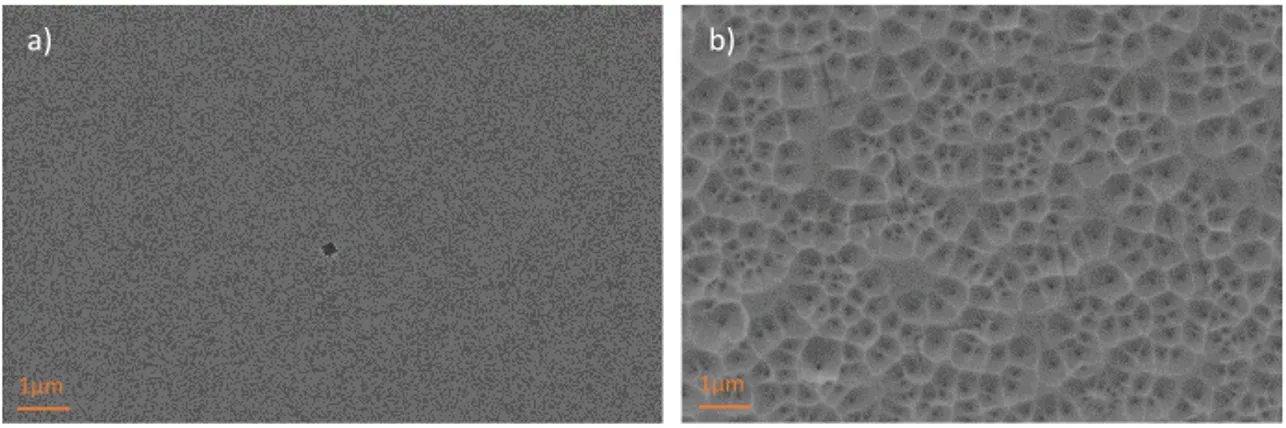
Similar TDD of 2×107cm−2was delineated after the etching in Secco and Iodine
solutions. Scanning electron microscope (SEM) images of the surface topography after defect selective etching are shown in figure 3.6. For further improvement of the crystal quality, the Ge buffer layers were grown on Si substrates by using digermane as the Ge precursor.
1µm 1µm
a) b)
Figure 3.6: Etch pit density of Ge SRB revealed by a) Iodine solution and b) Secco
solution
3.3.2
Ge growth using digermane
The lower activation energy of digermane compared to germane makes it possible to deposit the Ge seed layer at temperatures below 300℃. The growth rate of the Ge layer on Si substrate at temperatures ranging from 280°C to 600°C is shown in figure 3.7. The flow of digermane (10% diluted in hydrogen) was 100 SCCM, and the reactor pressure was kept at 20 Torr during the growth. By using digermane, the Ge layers are deposited at much higher rates compared to when germane is used. The lowest growth temperature decreased from 350°C to 280°C by using digermane instead of germane because of the lower activation energy of digermane when compared with that of germane. The activation energy of 1.1 eV was calcu-lated from the slope of the graph, which is in line with previous studies [36]. The reaction is in the kinetic regime at temperatures below 360°C, and the growth rate increases by increasing the temperature. At these temperatures, the deposition is controlled by chemical reactions on the surface, atoms’ mobility, and desorption of by-products. At temperatures above 360°C, however, the reaction happens in a diffusion-controlled regime that is limited by the mass flow of the reactants. There-fore, increasing the temperature does not increase the growth rate of the layers. At temperatures above 400°C, the higher gas-phase decomposition of digermane reduces the growth rate.