ACTIVE LIMITING FREQUENCY SELECTIVE SURFACE AT X-BAND
A thesis submitted to the Faculty and the Board of Trustees of the Colorado School of Mines in partial fulfillment of the requirements for the degree of Master of Science (Electrical Engineering). Golden, Colorado Date: _________________________ Signed: _________________________ Patrick Bay Signed: _________________________ Dr. Payam Nayeri Thesis Advisor Golden, Colorado Date: _________________________ Signed: _________________________ Dr. Peter Aaen Professor and Head Department of Electrical Engineering
ABSTRACT
Receivers used in wireless communication systems will commonly employ limiters to protect sensitive low-noise electronics from high-power emitters that may be located nearby. Receivers may be designed to operate with signals in the nanowatt (10-9 W) range, while nearby transmitters may be broadcasting hundreds or thousands of Watts of power. The disadvantage of traditional receiver limiters are that they are located downstream from the antenna, which will commonly have gain and increase the amount of power that the limiter must handle. A frequency selective surface with integrated limiter protection is proposed to mitigate this issue by moving the limiting function before the antenna, and this type of receiver protection has had minimal investigation in the existing literature. A new design operating at X-band is proposed using a square-plate element, and is simulated and measured for both small-signal and large-signal conditions. The measurements show that the concept is capable of non-linear limiting behavior with insertion loss comparable to the traditional microstrip limiter approach.
TABLE OF CONTENTS
ABSTRACT ... iii
LIST OF FIGURES ... vi
CHAPTER 1 BACKGROUND ... 1
1.1 Receiver Protection and Noise Sensitivity ... 1
1.2 PIN Diode Limiters ... 3
1.3 Frequency Selective Surfaces... 7
CHAPTER 2 PROPOSED DESIGN ... 11
2.1 Design Overview ... 11
2.2 Design Parameters ... 12
2.3 Similar Research ... 13
CHAPTER 3 DESIGN SIMULATION ... 16
3.1 Small-Signal Simulation Overview ... 16
3.2 Small-Signal Simulation Results ... 20
3.3 Sensitivity Analysis ... 27
3.4 Large-Signal Simulation ... 31
CHAPTER 4 TEST RESULTS ... 35
4.2 Test Fixture & Calibration ... 37
4.3 Small-signal measurements ... 39
4.4 Large-signal measurements ... 43
4.5 Beam-lead diode testing ... 44
CHAPTER 5 CONCLUSIONS AND FUTURE WORK ... 47
REFERENCES ... 48
LIST OF FIGURES
Figure 1.1 Traditional vs. proposed receiver block diagram. ... 2
Figure 1.2 PIN diode symbol, structure, and equivalent circuit. ... 3
Figure 1.3 PIN diode series switch ... 5
Figure 1.4 PIN diode limiter and equivalent small-signal circuit. ... 5
Figure 1.5 PIN limiter DC current path. ... 6
Figure 1.6 Anti-parallel PIN limiter configuration. ... 7
Figure 1.7 “Gangbusters” FSS. ... 8
Figure 1.8 Square-plate FSS and equivalent circuit... 9
Figure 1.9 Square-plate unit cell repeated through FSS. ... 9
Figure 2.1 Proposed FSS unit cell and schematic representation. ... 11
Figure 2.2 Electric field strength on FSS. ... 12
Figure 3.1 Unit cell and master / slave boundaries in HFSS Floquet analysis. ... 17
Figure 3.2 RLC surface to simulate diode. ... 18
Figure 3.3 Antenna in a 90° corner reflector and its images. ... 19
Figure 3.4 Simulation results, passive FSS, Floquet model. ... 21
Figure 3.6 Simulation results, passive FSS, waveguide model. ... 23
Figure 3.7 Simulation results, active FSS w/ MACOM, Floquet model. ... 24
Figure 3.8 Simulation results, active FSS w/ MACOM, waveguide model. ... 24
Figure 3.9 Size comparison of designs w/ MACOM & Microsemi Diodes. ... 25
Figure 3.10 Simulation results, active FSS w/ Microsemi, Floquet model. ... 26
Figure 3.11 Simulation results, active FSS w/ Microsemi, waveguide model. ... 26
Figure 3.12 Sensitivity analysis for azimuth (Φ) ... 27
Figure 3.13 Sensitivity analysis for elevation (Θ) ... 28
Figure 3.14 Diode labels for capacitance sensitivity analysis. ... 29
Figure 3.15 Shifting capacitance of all diodes. ... 29
Figure 3.16 Shifting capacitance of individual diodes. ... 30
Figure 3.17 Offsetting capacitance shifts... 31
Figure 3.18 Voltage measurement line across RLC surface. ... 33
Figure 3.19 Simulated non-linear responses using MACOM diode. ... 34
Figure 4.1 Gold pads on diode. ... 35
Figure 4.2 Assembled active FSS w/ Microsemi diodes. ... 36
Figure 4.5 Sample holder measurement after TRL calibration... 38
Figure 4.6 Passive FSS installed in sample holder. ... 39
Figure 4.7 Passive FSS, simulated vs. measured. ... 39
Figure 4.8 Active FSS w/ MACOM, simulated vs. measured. ... 40
Figure 4.9 Active FSS w/ Microsemi, simulated vs. measured. ... 41
Figure 4.10 Baseline microstrip limiter w/ MACOM diode. ... 41
Figure 4.11 Measured insertion loss of microstrip limiter w/ MACOM diode. ... 42
Figure 4.12 Measured insertion loss of microstrip limiter w/ Microsemi diode. ... 42
Figure 4.13 Non-linear response of active FSS w/ Microsemi diodes. ... 43
ACKNOWLEDGEMENTS
I would like to thank my committee members including Dr. Christopher Coulsten , Dr. Randy Haupt, and Dr. Payam Nayeri for their support with this research. I would also like to give a special thanks to Dr. Nayeri for his guidance and encouragement during this process.
CHAPTER 1 BACKGROUND
1.1 Receiver Protection and Noise Sensitivity
When deploying RF communications systems, it is often necessary to have receivers and transmitters located in close proximity to one another. One common example is a basestation tower for mobile telephone systems; even if a communication system is not actively transmitting, there may still be high-power transmitters present from other operators / carriers. Receivers typically use sensitive electronic devices designed for low RF input power levels, and can be damaged by high RF power levels if precautions are not taken in the design.
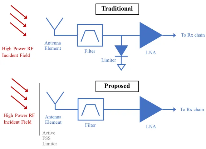
A well-designed receiver system will also include protection from high RF power levels, typically in the form of a PIN diode limiter [1]. It is commonly installed after any applicable filtering (so that it is not triggered by out-of-band signals) and before the first low-noise
amplifier (LNA), as shown in Figure 1.1. The disadvantages of this approach are increased loss before the LNA, and the fact that an antenna with gain can increase the amount of power that the limiter is required to handle. For example, a microstrip patch antenna element with a gain of 6 dB would more than double the amount of power that the limiter needed to handle compared to an ideal dipole antenna element. By integrating a limiter into a frequency selective surface (FSS) before the antenna, higher power handling may be possible.
Figure 1.1 Traditional vs. proposed receiver block diagram.
Noise performance of a receiver system is typically characterized by its noise figure (decibel form) or noise factor (linear form). The noise factor is given by the ratio of input to output signal-to-noise ratios [2]:
𝐹 = (𝑆 𝑁⁄ )𝐼
(𝑆 𝑁⁄ )𝑂 (1.1)
Thus, the noise factor / figure is a measure of how the signal-to-noise ratio degrades through a system. Passive devices such as limiters have a noise factor / figure that is equal to their loss, and the noise factor of a cascaded system is given by [2]:
F = F1 + (F2-1) G 1
⁄ + (F3-1)⁄G1G2+… (1.2)
Where Fn is the noise factor of the nth stage, and Gn is the gain of the nth stage. Components located after gain stages will have a lower contribution to the overall system noise, and any passive components located before the first gain stage will add a one-for-one contribution to the system noise figure based on their loss. Achieving good noise performance in a receiver requires minimizing any losses before the first amplifier, which includes limiter losses. If an active limiting FSS is to be used, the loss introduced relative to a standard passive FSS should be comparable or better than existing microstrip limiter approaches.
1.2 PIN Diode Limiters
PIN diodes are devices that are used in many common RF circuits, including switches, variable attenuators, and phase shifters. The schematic symbol is the same as a standard diode, as shown in Figure 1.2. The structure of a PIN diode is similar to a standard PN junction diode, but has an intrinsic region of undoped silicon in the center. The equivalent circuit for the PIN diode consists of a junction resistance RS, junction capacitance CJ, and package inductance LP.
At RF frequencies, the unbiased PIN diode will have no charge carriers in its I-region and can be represented by the junction capacitance CJ, along with a large value for the junction series resistance RS. Because the impedance of the junction resistance RS is significantly larger than the impedance of the junction capacitance CJ at high frequencies, the junction resistance can often be ignored and the diode can be modeled as a capacitor (neglecting any package parasitics).
Control of the PIN diode is achieved by applying a DC bias, which injects charge carriers into the I-region and allows the PIN diode to conduct. At RF frequencies, the diode effectively acts as a current-controlled resistor, where the DC bias current modulates the RF junction resistance RS. If the DC bias current sets the junction resistance to a small enough value, the junction capacitance may be ignored as its RF impedance is greater than the resistance and is effectively “shorted out” by the resistor.
Figure 1.3 shows an example of a typical use of a PIN diode as a series-element RF switch [3]. Inductors are used to “choke” the RF signal while allowing the DC bias signal to pass through, and the capacitors function as DC blocks while allowing the RF signal to pass through. When a DC bias is applied, the diode conducts and the RF impedance is small (1-2 Ω for
example), and the switch is “ON” (low loss). When the DC bias is removed, the diode is not conducting and the switch is “OFF” (high loss). Some small amount of RF energy will still leak through the switch due to the small parasitic capacitance of the diode in the “OFF” (high loss) state.
Figure 1.3 PIN diode series switch
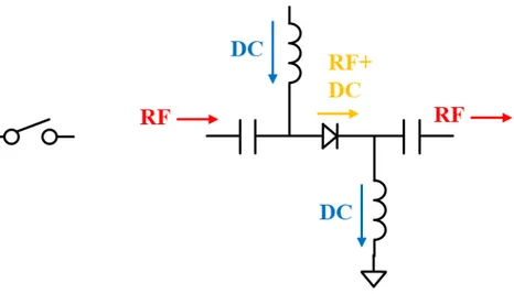
For a PIN diode limiter used for receiver protection, the diode is connected without any external DC bias. The most basic configuration of a PIN limiter is shown in Figure 1.4, where the diode is installed in a shunt configuration, and an inductor is also connected in a parallel shunt configuration. When small RF signals are present, charge carriers are injected into the I-region during one half of the RF cycle, and removed during the opposite cycle. The diode is unbiased and can be modeled as a parasitic capacitor.
Figure 1.4 PIN diode limiter and equivalent small-signal circuit.
Under large RF signal conditions, charges are again injected into the I-region during half of the RF cycle. During the opposite half of the RF cycle, most of the charge carriers are
removed from the I-region, but some of the carriers closer to the center of the I-region remain. When this process repeats for several RF cycles, enough charge carriers are present in the I-region such that the diode starts to conduct at RF frequencies, and the junction resistance RS is low [4]. When this occurs, the PIN diode starts to appear as a short circuit, and RF energy is reflected back toward its source. The inductor provides a return path for the charges flowing through the diode, and a DC current loop is formed as shown in Figure 1.5.
Figure 1.5 PIN limiter DC current path.
It is important to note that a PIN diode functions as a self-biased current-controlled resistor in the limiter case, and not as a “clipping” diode such as those installed for electrostatic discharge (ESD) protection in commercial integrated circuits. This allows the PIN diode limiter to provide higher levels of isolation (protection) than a diode intended for rectifying / clipping (e.g. Schottky diode) [4].
The inductor in Figure 1.5 provides a DC return path for the charge carriers flowing through the PIN diode. An alternative approach is the anti-parallel configuration shown in Figure 1.6. In this configuration, 2 PIN diodes are installed with opposite polarities such that the
Figure 1.6 Anti-parallel PIN limiter configuration.
1.3 Frequency Selective Surfaces
As the name implies, a frequency selective surface (FSS) allows some RF frequencies to pass through with low loss, and rejects others by reflecting the propagating waves back toward their source. They can be viewed as a surface that provides RF filtering, and most commonly use the band-pass and band-stop response types.
A FSS can be implemented using standard printed circuit board (PCB) technology, whereby a conductive pattern is etched on a copper-clad substrate. More complex FSSs can be formed by using multiple conductive layers with different patterns.
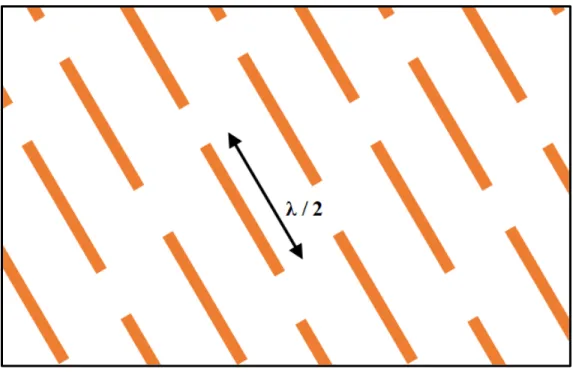
One of the simplest FSS types is the “gangbusters” design [5] shown in Figure 1.7. This design uses an array of dipole elements to form a bandpass response; the frequency where the dipole is a half wavelength long will pass through the surface. The type number (density) of the elements can be increased to form a narrower bandpass response. Although this FSS element is very simple to implement, it does not lend itself to easy integration of active electronic
Figure 1.7 “Gangbusters” FSS.
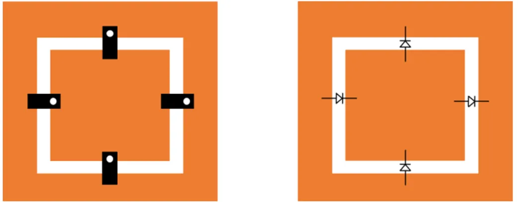
Another FSS element with a bandpass response is the loaded square plate element shown in Figure 1.8. In this element, the square plate in the center forms a capacitive coupling to the outer plane, and the narrower portions of the outer plane form a series inductance. The total element forms a LC resonant circuit that determines the location of the passband [5]. The
structure of this element type makes it easier to integrate with active electronic components, and its symmetry also makes it more stable with respect to the polarization and angle of incidence of incoming RF waves. The simple geometry makes it easy to fabricate, and it is less prone to manufacturing problems such as trace peeling that affect a design with thin traces like the Gangbusters FSS.
Figure 1.8 Square-plate FSS and equivalent circuit.
A FSS is a periodic structure, and the single element shown in Figure 1.8 forms the unit cell that is repeated over the entire surface. An ideal FSS would repeat the unit cell pattern infinitely in both directions.
It is important to note that a FSS is typically bounded by free space on at least one side, where the fields have the free-space impedance given by [6]:
η0= √μ0 ε 0
⁄ ≈ 377 Ω (1.3)
When an incident wave encounters a boundary with a different dielectric constant (such as a PCB substrate), some of the energy is reflected back toward the source. The reflection coefficient is given by [6]:
Γ= (η - η0)
(η + η0)
⁄ (1.4)
For this reason, it is desirable to use a PCB material with a low dielectric constant in order to minimize unwanted reflections from the substrate, so that the desired reflections from the conductive pattern dominate the FSS response.
CHAPTER 2 PROPOSED DESIGN
2.1 Design Overview
The proposed design for the active limiting FSS is shown in Figure 2.1. It uses the square-plate structure for a bandpass response, and PIN diodes are installed across the gap between the center plate and outer plane. Because the diodes can be modeled as a capacitor under small-signal conditions, they serve to supplement the capacitance between the center plate and outer plane that is normally part of the design (shown previously in Figure 1.8). This has some benefit in reducing the size of the design, which has been investigated with a different strategy for this FSS topology in [7]. Additionally, the diodes form an anti-parallel pair in each polarization direction, providing the DC return paths necessary for high-power limiting
conditions.
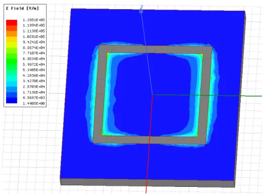
As shown in Figure 2.2, the electric field strength is highest near the centers of the square edges of the FSS. To provide the highest limiting action, the diodes are installed in this location in order to short out the electric field where it is strongest with high-power incident fields.
Figure 2.2 Electric field strength on FSS. 2.2 Design Parameters
There are several parameters that must be selected in the design of the active FSS. First, the size of the unit cell is selected to be approximately λ / 4 at the center of the passband, as mentioned in [5]. Some minor tweaking of the size may be needed when the supporting PCB material is added to the model, depending on its dielectric constant. This design was initially fabricated on Rogers 4350B material with a thickness of 0.762 mm (.030 inch) to utilize a
low-Next is diode selection. Because this design was intended to operate at X-band, it was necessary to find a diode with a small package and low package parasitics (inductance and capacitance). Because larger values of diode capacitance will increase the capacitive coupling between the outer plane and center plate, the size of the center plate must be reduced to reduce its contribution to the overall capacitance as the diode capacitance is increased. For this reason, selecting a diode with a low capacitance will help prevent the size of the center plate from shrinking to an unreasonably small size. For this design, the MEST2GFC-010-25 diode from MACOM and the MPL4700-206 diode from Microsemi were selected.
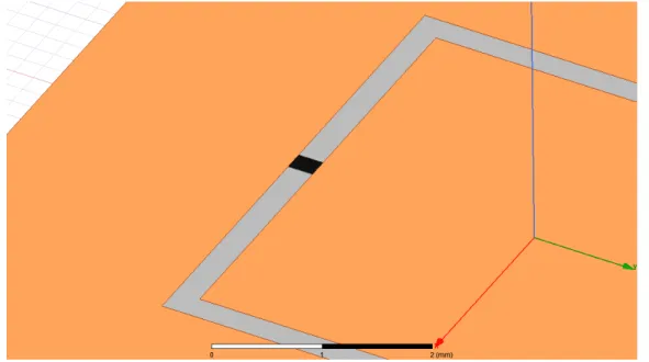
The gap between the center plate and outer plane will affect the coupling and
capacitance, but selection of the gap size is limited by the footprint of the selected diode. For this design, the size of the diodes was approximately equal to the EIA 0402 (Microsemi) and 0201 (MACOM) case sizes, so a gap of 0.254 mm (.010 inch) was used. The passive design variant without diodes does not have the same constraint, and a spacing of 0.5 mm (.020 inch) was chosen.
Once all of the other parameters have been selected, the size of the center patch is adjusted to fine-tune the frequency of the desired passband. This adjustment is done during the simulation process.
2.3 Similar Research
Currently, there is minimal research into power-limiting FSSs. An early example of this application is forming a RF “shutter” through the use of electrostatic switches, described in [8]. A primary disadvantage of this approach is that it requires an external control voltage in order to activate the switches, and is more applicable to protection of a transmitter than a receiver since a
receiver will have no a priori knowledge of when an incoming signal will be received. Additionally, while the author discusses the potential application of the device on an airplane wing, the use of electromechanical switches in a high-vibration environment would present a reliability concern.
Similar to the above, another proposed design in [9] is for an active FSS using PIN diodes that are externally biased to form a RF “shutter.” The design is simulated for operation in the ISM band at 2.45 GHz. While this design is potentially more rugged due to the solid-state nature, it still requires a priori knowledge of a potential high-power signal for receiver
applications. It could potentially be useful in an application that is transmit-only, when the system has knowledge of when to “open” the RF shutter based on the transmit waveform.
Using PIN diodes to provide reconfigurability for polarization or frequency of operation has received more attention in the literature. Reconfigurability of polarization of a patch antenna is shown in [10], while [11] and [12] show active components being used to change the operating frequency.
A more recent example of a power-limiting FSS is given in [13]. In this design, a resist material consisting of Vanadium dioxide is placed across the FSS surface. Under small-signal conditions, the Vanadium dioxide presents a high resistance and does not interfere with normal operation of the FSS. In the presence of a high-power RF signal, the Vanadium dioxide heats up until it undergoes a phase change and its resistance is lowered, shorting out the FSS and
reflecting the high-power incident signal. The advantage of this approach is that it is completely passive like a traditional limiter. However, because the limiting action is dependent on a
The closest designs to the proposed are a limiter using metamaterials in [14], and an active FSS using PIN diodes described in [15]. The FSS design uses loop elements for the FSS structure, and also needed to be retuned to compensate for the capacitive loading of the diodes. The authors chose the loop element for the angular stability, but it does require a more intricate PCB artwork that will be more difficult to fabricate at higher frequencies. This design operated in the center of S-band at 3 GHz.
CHAPTER 3 DESIGN SIMULATION
3.1 Small-Signal Simulation Overview
Small-signal modeling of the FSS was conducted in the High Frequency Structure Simulator (HFSS) package from Ansys, which is a 3D electromagnetic solver. Because of the difficulty of simulating a large or infinite array, the software has capabilities of performing a Floquet analysis that allows the FSS to be simulated at the unit cell level.
Floquet theory is used to find the solution of a periodic set of differential equations (including the differential form of Maxwell’s equations), and the resulting solution is also periodic [16]. To perform Floquet analysis within HFSS, “master” and “slave” boundaries are used at the edges of the unit cell. HFSS will force the solutions of Maxwell’s equations to be equal for each master and slave boundary pair, resulting in a periodic solution to the analysis. This allows HFSS to analyze the structure in the unit cell as it would appear in an infinite array.
Additionally, the phase relationship between each master and slave boundary can be specified in order to simulate different scan angles (i.e. angles of incidence). Setting these angles to project-wide variables will allow a swept analysis to be performed using the Optimetrics feature within HFSS [17].
Figure 3.1 Unit cell and master / slave boundaries in HFSS Floquet analysis.
HFSS is typically only used to model passive structures, so active devices such as diodes are usually not included. As mentioned in paragraph 1.2, diodes may be modelled as capacitors under small-signal conditions. To include the diodes in the HFSS simulation, a RLC surface impedance was placed across the gap between the outer plane and inner plate at each of the diode locations. To simplify the model, only the junction capacitance was included in the RLC surface, and a 2nd RLC surface to model the series inductance of the package was not included.
Figure 3.2 RLC surface to simulate diode.
Although Floquet analysis is extremely useful for analyzing a periodic structure in an infinite array, it does not provide an easy means of testing the design as an infinite array cannot be realized in practice. Testing the FSS in a manner that replicates the behavior in an infinite array requires the use of waveguide as a test fixture. To illustrate how a waveguide fixture can be used to simulate an infinite array, consider how an antenna placed within a 90° corner reflector with perfect conductor walls will produce “images” of the original antenna. The solution of the EM fields is equivalent to that of the sum of the fields of the original antenna and the fields from its images [18]. Similarly, placing the FSS unit cells inside a waveguide cavity with conductive walls will produce images of the original FSS and simulate the unit cell in an infinite array.
Figure 3.3 Antenna in a 90° corner reflector and its images.
It should be noted that when simulating or testing the FSS in a waveguide, the incident plane waves may not necessarily be at boresight (i.e. zero scan angle) because waveguide typically relies on a transverse electric mode of propagation (TE10 mode) instead of the transverse electromagnetic (TEM) mode of propagation used by other structures such as microstrip. For waveguide, the scan angle is given by [19]:
sin 𝜃 = 𝜆 𝜆𝐶⁄ (3.1)
where θ is the scan angle, λ is the test frequency wavelength, and λC is the wavelength of the waveguide cutoff frequency. For this reason, the angular stability of the FSS design will contribute to the simulated and measured performance over frequency in waveguide, since the scan angle will vary as a function of frequency.
As is common in RF circuits, scattering parameters (S-parameters) are used as the figures of merit for small-signal conditions. The FSS can be considered to be a 2-port device, since energy incident on it will either be reflected (as measured by the magnitude of S11) or
terms used to refer to the magnitudes of S11 and S21 respectively, though they are opposite in sign (and defined as positive quantities). The FSS is a passive, reciprocal device, so S22 and S12 may be neglected in the analysis since they are equal to S11 and S21 respectively.
3.2 Small-Signal Simulation Results
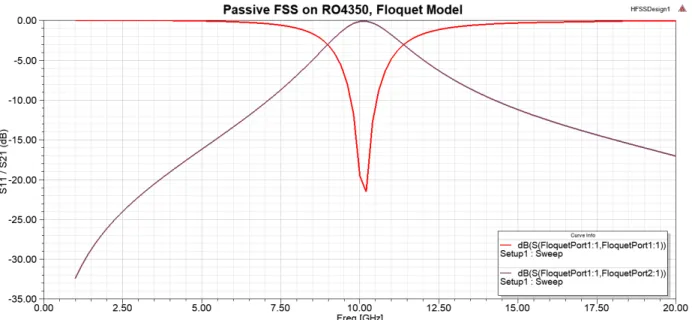
All the designs in this research used a target operating frequency of 10 GHz (the center of X-band). A passive FSS without diodes was modeled first, and is used as a baseline for
comparison. For the 0.762 mm thick RO4350B substrate and a center plate gap of 0.5 mm, a center plate size of 5.6 mm in each direction resulted in a passband centered at 10 GHz. The results shown in Figure 3.4 show that the magnitude of S11 is minimized and the magnitude of S21 is maximized at 10 GHz, indicating that most of the energy is transmitted through (S21) with minimal energy reflected (S11) at that frequency but the FSS provides rejection via reflection (low S21 / high S11) at other frequencies.
Figure 3.4 Simulation results, passive FSS, Floquet model.
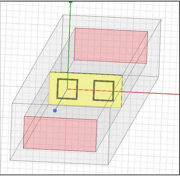
Next, the FSS is simulated in a waveguide cavity to more closely resemble the final test configuration. WR-90 waveguide has a recommended operational frequency range of 8.2 to 12.4 GHz, making it a good selection for the target operating frequency. The inner dimensions of 22.86 mm (.900 inch) by 10.16 mm (.400 inch) allow two unit cells to be placed in the waveguide cavity, as shown in Figure 3.5.
Figure 3.5 Simulation model, passive FSS in waveguide.
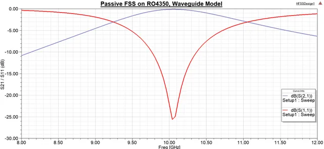
No adjustments to the center plate size were required to keep the design centered at 10 GHz in the waveguide model, as shown in Figure 3.6.
Figure 3.6 Simulation results, passive FSS, waveguide model.
The active FSS designs with diodes follow the same process as the passive design. For the design with the MACOM MEST2GFC-010-25 diodes, the datasheet capacitance of 0.04 pF typical @ VR = -10V is used. It should be noted that although a reverse bias is not applied to the diodes when installed on the FSS, the datasheet capacitance under reverse bias should be used in the model because the datasheet capacitance is measured at a much lower frequency (1 MHz), and the capacitance at this frequency under reverse bias is more representative of the capacitance at microwave frequencies and zero bias due to the punch-through effect [4].
The size of the center plate is reduced from the 5.6 mm passive design size to 5.092 mm in order to compensate for the additional capacitance from the diodes. No adjustment was made in the design from the Floquet model to the waveguide model, but the waveguide model did show some small ripples in the insertion loss and return loss that were not present in the Floquet model. By comparing Figure 3.4 and Figure 3.7, it can also be seen that the passband is narrower for the active design than for the passive design.
Figure 3.7 Simulation results, active FSS w/ MACOM, Floquet model.
A second design using the Micosemi MPL4700-206-HS was also simulated. The
datasheet for this part specifies a CP = 0.04 pF typical and CT = 0.15 pF typical, so a capacitance of 0.12 pF was used for the simulation. To keep the passband centered at 10 GHz, the size of the center plate is further reduced to 4.09 mm. A comparison is shown in Figure 3.9 illustrating how the increased capacitance further reduces the plate size. The simulated performance in the Floquet model and waveguide model is shown in Figure 3.10 and Figure 3.11 respectively. One interesting effect of the increased capacitance is a narrowing of the bandwidth, which can be seen by comparing Figure 3.11 with the MACOM design in Figure 3.8. An even sharper contrast is visible when comparing to the passive design in Figure 3.6.
Figure 3.10 Simulation results, active FSS w/ Microsemi, Floquet model.
3.3 Sensitivity Analysis
As mentioned previously, the scan angle incident on the device under test will vary with frequency when testing the design in waveguide. Having a design that is stable with angle of incidence of incoming waves is critical to obtaining good test results in the waveguide fixture. The optimetrics feature in HFSS can be used to sweep the azimuth and elevation scan angles [17] during Floquet modeling. For this design, each of the scan angles was varied from 0 to 45° in steps of 11.25°. As shown in Figure 3.12 and Figure 3.13, the design is quite stable with angle of incidence.
Figure 3.13 Sensitivity analysis for elevation (Θ)
Each of the design simulations used the same value of capacitance for all 4 diodes (or 8 diodes in the case of waveguide models). For fabricated hardware, some amount of variation in capacitance between diodes can be expected, so the effects of these variations were investigated using the Floquet model of the design with MACOM. A variation of ±0.005 pF (±12.5%) was used for the capacitance sensitivity analysis. Diodes typically have less unit-to-unit variations in performance between pieces from the same manufacturing lot, so small variations in the
sensitivity analysis are appropriate. For this simulation, the diode capacitances were individually adjusted using the labeling scheme shown in Figure 3.14.
Figure 3.14 Diode labels for capacitance sensitivity analysis.
As expected, shifting the capacitances of all diodes equally resulted in a shift of the passband frequency as shown in Figure 3.15. Note that the nominal design is centered at 10.6 GHz in this simulation (it was simulated using a Rogers 5880 PCB substrate, so the response is slightly different than shown in Figure 3.7). An adjustment of ±0.005 pF to all diodes resulted in a frequency shift of approximately ±150 MHz.
When the diodes are individually adjusted, changing the values of C1 and C2 had no effect on the center frequency of the passband. Changing the value of C3 or C4 did result in a shift to the passband of approximately 75 MHz, and changing the value of both C3 and C4 resulted in the full shift of 150 MHz. These results are shown in Figure 3.16 for a lower capacitance shifting the response up-frequency, but the same effect occurs in the opposite direction (i.e. response shifts down-frequency) when the diode capacitances are increased.
Figure 3.16 Shifting capacitance of individual diodes.
Because the capacitance of C3 and C4 had the most effect on the center frequency of the passband, the effect of offsetting capacitances was investigated on these diodes. The simulation showed that offsetting capacitances would result in no shift to the passband, as plotted in Figure 3.17. The capacitances of diodes in a real FSS would likely follow a normal distribution, and so the mean capacitance would likely shape the frequency response in a real array. When simulating
using Floquet analysis, any errors introduced are periodic in nature and may not reflect the real performance of the array.
Changing the Floquet simulation with the azimuth scan angle Φ rotated by 90° shows the same results, but with C1 and C2 showing the same frequency shift due to capacitance change instead of C3 and C4. Based on this result, we can expect that any frequency shift due to capacitance variation in a full array will be dependent on the polarization of the incident wave.
Figure 3.17 Offsetting capacitance shifts. 3.4 Large-Signal Simulation
Simulating the non-linear performance of PIN diode circuits is difficult because
manufacturers typically do not provide non-linear models of their devices, and modeling must be performed with the limited characteristics provided on a datasheet. The resistance of a PIN diode under self-biasing high-power conditions is given by:
R= h β√D ω⁄ √
Z0
where h is the I-region thickness in cm, β = q/kT = 40, D is the diffusion coefficient (15.6 cm2/sec, Pi is the incident pulse power, and ω is the frequency in radians [20]. However, this assumes the diode is installed in a typical transmission line structure (e.g. microstrip) with a defined characteristic impedance. In the case of a FSS, no such characteristic impedance can be used.
Additionally, EM tools such as HFSS do not provide non-linear analysis tools such as harmonic balance solvers. To work around these problems, a Matlab script for performing non-linear analysis was created to use data inputs from HFSS. An equation from [4] relating the diode resistance to current in limiter applications is used:
RI= w√F 20×I⁄ RF (3.3)
where RI is the diode resistance in Ohms, w is the I-region width in microns, and IRF is the microwave current in ARMS.
An optimetrics sweep was set up in the HFSS simulation to vary diode resistance and measure the corresponding voltage across the resistor. The resistor value was included in the same RLC surfaces used previously, and a measurement line was set up across the RLC surface. The HFSS fields calculator was used to measure the voltage across the RLC surface for each swept value of diode resistance. All measurements were done using the HFSS default power level of 1 W. Changing the default power level in HFSS simply results in a linear scaling factor being applied to the results, so it was not necessary to modify the power level in the simulation because it can be scaled afterward in the nonlinear model.
Figure 3.18 Voltage measurement line across RLC surface.
The table of HFSS simulated diode resistance vs. voltage and S21 was loaded into a Matlab script which sweeps the RF input power by applying a linear scaling factor to the HFSS voltage / current. The diode resistance and current are interdependent and as such cannot be solved directly. To calculate the diode resistance and current at each power level, an iterative solver is used with an initial guess of the diode resistance in order to calculate the current, and then makes adjustments until the equation relating diode resistance to current is satisfied within an acceptable error tolerance. This allows the input / output power compression curve to be calculated with the I-region thickness as the only required diode parameter.
A similar script was created for simulating diodes in a standard microstrip configuration. This script uses standard closed-form equations for calculating the diode voltage and current instead of interpolating from HFSS results. A comparison of the simulated non-linear responses for the microstrip and FSS configurations using the MACOM diode is shown in Figure 3.19. The simulations predict that the FSS will have a lower compression point than a standard microstrip
CHAPTER 4 TEST RESULTS 4.1 FSS Assembly
Before testing the active FSS, the diodes must be installed onto the FSS PCB. As
discussed previously, the diodes used in the initial design and simulation were selected based for their low values of package parasitics (including capacitance). However, these attributes are achieved by using “flip chip” style packaging instead of standard plastic packages for the diode die. These packages also use pure gold metallization for their interconnects instead of plated copper leads used in plastic packages.
Figure 4.1 Gold pads on Microsemi diode.
The tin present in standard tin-lead or RoHS solders tends to scavenge any gold present during solder reflow [21]. This is normally not a problem when gold is used as an anti-corrosion surface finish (such as in the electroplated nickel, immersion gold, or ENIG, surface finish commonly used for PCBs) since the solder joint will form to the underlying metal. However, since gold is the only metallization for the diodes used in the FSS, any tin present in the solder
would remove the only metallization present and no solder joint would form. For this reason, a non-standard indium-lead solder alloy needed to be used for assembly, which made the assembly process more difficult.
The indium-lead solder did not have any problems with gold scavenging, but it did seem to be more difficult to get good adhesion to the gold in the diodes, even when using the included flux. This was less of a problem with the Microsemi diodes due to their larger overall size and larger land pads, and the active FSS was successfully assembled as shown in Figure 4.2.
Figure 4.2 Assembled active FSS w/ Microsemi diodes.
For the MACOM diodes, the smaller package size and smaller land pads made the
assembly even more difficult, and attempts to solder the diodes were unsuccessful. To get around this problem, attachment of the diodes using conductive silver epoxy was attempted, as shown in Figure 4.3. This resulted in some of the diodes being connected successfully, while the others
then more epoxy was added to the open-circuit diodes to try to connect them. However, this resulted in excess epoxy forming short-circuits at the diodes and rendering the prototype unusable for further testing. More advanced manufacturing methods such as gold-tin eutectic attach may be required for proper installation of these parts, but such methods were not possible and not attempted for this build.
Figure 4.3 Silver epoxy attachment of MACOM diodes.
4.2 Test Fixture & Calibration
As mentioned previously, a WR-90 waveguide fixture is used for testing the FSS structure. Each half of the test fixture consists of a SMA-to-waveguide adapter followed by a 100 mm length of straight waveguide. A small center section of waveguide is used as a sample holder and is designed for holding PCBs that are 1.57 mm (.062 inch) thick.
To remove the effects of the waveguide adapter in the measurement results, a thru-reflect-line (TRL) calibration was performed with the waveguide adapters in place to remove their effects. The calibration standards used were a 9.75 mm length of waveguide and a flat block to create a short. After performing the calibration, the sample holder was inserted into the setup
to measure its performance. The sample holder measured more than 34 dB of return loss (S11) across the band, indicating a good match and good calibration.
4.3 Small-signal measurements
After calibrating the test fixture, the passive FSS was measured first to establish a
baseline. The FSS installed in the sample holder is shown in Figure 4.6. The passive FSS showed excellent agreement between the simulated and measured results and very low loss (0.3 dB) as shown in Figure 4.7.
The active FSS with MACOM diodes was measured next. As mentioned previously, not all of the diodes were properly connected in the FSS; some of the diodes were open-circuit. From Figure 4.8 it can be seen that although the center frequency is within 5% of the target passband, the loss is significantly higher at approximately 2.8 dB. If all the diodes were connected, the additional capacitance would likely move the passband response further down-frequency.
Figure 4.8 Active FSS w/ MACOM, simulated vs. measured.
Finally, the design with the Microsemi diodes was measured. Unlike the prototype with the MACOM diodes, the FSS with the Microsemi diodes did have all diodes connected properly. The measured response showed the passband was significantly down-frequency from the 10 GHz target, indicating that the diode capacitance is likely higher than simulated. This design also
Figure 4.9 Active FSS w/ Microsemi, simulated vs. measured.
Limiters using the standard microstrip configuration were also fabricated in order to provide a baseline for comparison. The microstrip limiter using the MACOM diode along with a DC return coil is shown in Figure 4.10, and its measured insertion loss is shown in Figure 4.11. The insertion loss measured 0.6 dB at 10 GHz. The same circuit using a Microsemi diode showed slightly higher loss (0.7 dB) as shown in Figure 4.12.
Figure 4.11 Measured insertion loss of microstrip limiter w/ MACOM diode.
4.4 Large-signal measurements
Next, the non-linear response of the FSS with Microsemi diodes was measured. The measurement was performed by connecting a RF signal generator to the input via a coupler and power sensor to monitor input power, and a 2nd power sensor connected to the output. The measured response is shown in Figure 4.13. A comparison of the measured & simulated
responses of the microstrip coupon are shown in Figure 4.14. Both the simulated and measured results show that the compression point is lower for the active FSS configuration than the microstrip configuration when using the same diode. For both circuits, it appears that package inductance may be affecting the attenuation of the limiter and causing a larger discrepancy between measured and simulated results at higher power levels.
Figure 4.14 Non-linear response of microstrip limiter w/ Microsemi diodes.
4.5 Beam-lead diode testing
Because the MACOM and Microsemi diodes did not show the desired performance at X-band, another FSS was built and tested using the Skyworks DSG9500-000 beam-lead diode. This diode is extremely small (0.28 x 0.18 mm / .011 x .007 inch) and utilizes gold ribbons for
interconnects, which results in very low package parasitics. The diode junction has a very low capacitance of 0.025 pF. This diode was tested on one of the PCBs intended for use with the MACOM diode as shown in Figure 4.15.
Figure 4.15 PCB with beam-lead diodes.
The lower parasitics of the beam-lead diode did result in improved small-signal
performance. The measured insertion loss of this configuration was 1.1 dB, which is significantly better than the loss measured with the other diodes, and the passband frequency was closer to the original 10 GHz target.
The beam-lead diode has a larger I-region width than the other diodes, and has a higher input compression point that is more difficult to measure due to the higher RF power levels required for test. The measured input 1 dB compression point was approximately +27 dBm (0.5 W) as shown in Figure 4.17, which was significantly higher than the simulation model. The compression characteristics do not show a trend back toward linear behavior like the Microsemi diode, but since the test data only captures a limited portion of the compression curve it is difficult to tell how the compression curves compare.
CHAPTER 5
CONCLUSIONS AND FUTURE WORK
An active limiting FSS operating at X-band was designed, simulated, and tested; the active limiting FSS previously demonstrated in the literature was only tested to approximately 4 GHz. When using diodes with low parasitic values, good small-signal insertion loss can be achieved with a passband close to the simulated value. The active FSS prototypes tested did show the desired non-linear behavior and achieved approximately 8 dB of compression for the Microsemi diode. Measured results agreed with the conclusion shown by simulations that the compression point of the FSS is lower than a traditional microstrip limiter when using the same diode.
Future investigations into this work might include testing with other low-parasitic diodes with different compression characteristics, as well as characterizing the RF power handling capability of this approach as compared to the traditional microstrip limiter approach.
REFERENCES
[1] R. Cory, "PIN-Limiter Diodes Effectively Protect Receivers," Electrical Design News, pp. 59-64, 17 December 2004.
[2] S. A. Maas, Noise in Linear and Nonlinear Circuits, Norwood: Artech House, 2005, pp. 36-39.
[3] Microsemi, PIN Diode Handbook, Version 2 ed., Watertown: Microsemi, 1999, pp. 3-4.
[4] J. F. White, Microwave Semiconductor Engineering, New York: Van Nostrand Reinhold, 1982, pp. 43-48,245-255.
[5] B. A. Munk, Frequency Selective Surfaces: Theory and Design, New York: Wiley, 2000, pp. 28-32, 52-53.
[6] D. M. Pozar, Microwave Engineering, Third Edition ed., Hoboken: Wiley, 2005, pp. 16, 27-29.
[7] B.-q. Lin, S.-h. Zhou, X.-y. Da, Y.-w. Fang, Y.-j. Li and W. Li, "Compact miniaturised-element frequency selective surface," Electronics Letters, pp. 883-884, 15 June 2015.
[8] H. C. Nathanson, M. C. Driver and R. J. Betsch, "High Attenuation Broadband High Speed RF Shutter and Method of Making Same". United States Patent 4,922,253, 1 May 1990.
[9] G. I. Kiani, K. P. Esselle, A. R. Weily and K. L. Ford, "Active Frequency Selective Surface Using PIN Diodes," in IEEE Antennas and Propagation Society International Symposium, Honolulu, 2007.
[10] W. Lin and H. Wong, "Polarization Reconfigurable Aperture-Fed Patch Antenna and Array," IEEE Access, vol. 4, pp. 1510-1517, 2016.
[11] M. Bouslama, M. Traii, T. A. Denidni and A. Gharsallah, "Active Antenna Based on a New Cylindrical Frequency Selective Surface," in Mediterranean Microwave Symposium, Marseille, 2017.
[12] M. Bouslama, M. Traii, G. Ali and T. A. Denidni, "Reconfigurable Dual-Band 3D Frequency Selective Surface Unit-Cell," in IEEE International Symposium on Antennas
and Propagation & USNC/URSI National Radio Science Meeting, Vancouver, 2015.
[13] S. Scott, C. D. Nordquist, M. J. Cich, T. S. Jordan and C. T. Rodenbeck, "A frequency selective surface with integrated limiter for receiver protection," in Proceedings of the 2012
IEEE International Symposium on Antennas and Propagation, Chicago, 2012.
[14] A. R. Katko, A. M. Hawkes, J. P. Barrett and S. A. Cummer, "RF Limiter Metamaterial Using p-i-n Diodes," IEEE Antennas and Wireless Propagation Letters, vol. 10, pp. 1571 - 1574, 2011.
[15] S. Monni, D. J. Bekers, M. van Wanum, R. van Dijk, A. Neto, G. Gerini and F. E. van Vliet , "Limiting Frequency Selective Surfaces," in Proceedings of the 39th European
Microwave Conference, Rome, 2009.
[16] Wikipedia, "Floquet Theory," Wikipedia, [Online]. Available:
https://en.wikipedia.org/wiki/Floquet_theory. [Accessed 7 September 2020].
[17] N. Appannagaari, I. Bardi, R. Edlinger, J. Manges, M. Vogel and Z. Cendes, "Modeling Phased Array Antennas in Ansoft HFSS," in IEEE International Conference on Phased
Array Systems and Technology , Dana Point, 2000.
[18] C. A. Balanis, "Antenna Theory: Analysis and Design," 4th Edition ed., Hoboken, Wiley, 2016, pp. 876-880.
[19] P. W. Hannan and M. A. Balfour, "Simulation of a Phased Array Antenna in Waveguide,"
IEEE Transactions on Antennas and Propagation, vol. 13, no. 3, pp. 342-353, 1965.
[21] Indium Corporation, "Soldering to Gold," [Online]. Available:
https://www.indium.com/technical-documents/application-notes/download/10/. [Accessed 7 September 2020].
APPENDIX
SUPPLEMENTAL ELECTRONIC FILES
PIN_limiter_compression_FSS.m MATLAB script for calculating the non-linear behavior of the active FSS.