Research article
Mahtab Aghaeipour and Håkan Pettersson*
Enhanced broadband absorption in nanowire
arrays with integrated Bragg reflectors
https://doi.org/10.1515/nanoph-2017-0101
Received October 13, 2017; revised December 9, 2017; accepted January 8, 2018
Abstract: A near-unity unselective absorption spectrum is desirable for high-performance photovoltaics. Nano-wire (NW) arrays are promising candidates for efficient solar cells due to nanophotonic absorption resonances in the solar spectrum. The absorption spectra, however, display undesired dips between the resonance peaks. To achieve improved unselective broadband absorption, we propose to enclose distributed Bragg reflectors (DBRs) in the bottom and top parts of indium phosphide (InP) NWs, respectively. We theoretically show that by enclosing only two periods of In0.56Ga0.44As/InP DBRs, an unselective 78% absorption efficiency (72% for NWs without DBRs) is obtained at normal incidence in the spectral range from 300 nm to 920 nm. Under oblique light incidence, the absorption efficiency is enhanced up to about 85% at an incidence angle of 50°. By increasing the number of DBR periods from two to five, the absorption efficiency is further enhanced up to 95% at normal incidence. In this work, we calculated optical spectra for InP NWs, but the results are expected to be valid for other direct band gap III–V semiconductor materials. We believe that our pro-posed idea of integrating DBRs in NWs offers great poten-tial for high-performance photovoltaic applications. Keywords: light trapping; distributed Bragg reflectors (DBRs); nanowires; photovoltaics.
1 Introduction
Nanowire (NW) arrays are intensively investigated for their potential use in photodetectors [1–4] and photovol-taics [5, 6] due to absorption of excited optical modes. In order to optimize the photovoltaic efficiency of NW array solar cells, it is important to engineer and rein-force absorption of the relevant excited optical modes to achieve an enhanced broadband light absorption in the solar spectrum. NWs support resonant optical modes due to their comparable dimensions to optical wavelengths [5, 7, 8]. One well-known strategy to enhance absorption is by tailoring the NW geometry [7–10], e.g. for an identi-cal diameter, by increasing the NW length and decreasing the distance between the NWs (pitch of the array). Such methods, however, lead to significantly increased mate-rial consumption. Moreover, the dark current in NW-based solar cells typically increases with NW length, which in turn reduces photovoltaic efficiency [11]. Another strat-egy to improve the absorption characteristics in NWs is to break the symmetry of the NW array/light incidence system [12]. Invoking oblique light incidence conditions improves absorption due to excitation of new polariza-tion-dependent optical modes [12, 13]. The improvement is, however, limited to relatively narrow regions of the solar spectrum [12]. To obtain further enhanced absorp-tion for identical geometry of the NWs in a broad spectral range, light trapping mechanisms have been invoked to reduce transmission through the NW/substrate interface [5] and light reflection at the superstrate/NW interface [14– 16] and to enhance the absorption in the NWs [17–19]. An ultimate strategy would offer strong absorption through-out the solar spectrum; wherefore, novel light trapping mechanisms [20] need to be explored in order to improve the solar cell efficiency [21, 22].
In this theoretical study, we propose to integrate axially distributed DBRs in the NWs as wavelength-selec-tive mirrors that efficiently trap the light inside the NWs and strongly suppress the leakage of light into the sub-strate [23]. An increased optical path length of the excited modes, due to multiple round trips in the DBR-NWs as a result of multi-reflection from the DBRs, leads to enhanced
*Corresponding author: Håkan Pettersson, Solid State Physics and
NanoLund, Lund University, Box 118, SE-22100 Lund, Sweden; and Department of Mathematics, Physics and Electrical Engineering, Halmstad University, Box 823, SE-301 18 Halmstad, Sweden, e-mail: hakan.pettersson@hh.se. http://orcid.org/0000-0001-5027-1456
Mahtab Aghaeipour: Solid State Physics and NanoLund, Lund
University, Box 118, SE-22100 Lund, Sweden
absorption and enhanced photovoltaic efficiency without the drawbacks of, e.g. increased dark current observed in elongated NWs [11]. Moreover, by properly optimizing the position of DBRs in the NWs, in addition to employing oblique incident light conditions, a near-unity absorption can be achieved throughout most of the solar spectrum. It should be noted that the embedded DBRs might poten-tially act as traps for the photogenerated charge carriers. In a recent report from our group, we showed, however, that InP NW photodetectors with embedded axial InAsP quantum discs with relatively deep confining potentials along the NWs exhibit excellent electro-optical properties at room temperature [4]. The high electric field strength in a typical p-i-n geometry of the NWs is likely to efficiently collect the photogenerated carriers. The proposed design of realizing integrated DBRs in NWs offers a novel promis-ing route to realize enhanced broadband absorption and photovoltaic efficiency in photodetectors and solar cells.
2 Calculations
In this work, we consider square arrays of vertically stand-ing InP NWs containstand-ing two absorbstand-ing DBRs compris-ing two (or five) alternatcompris-ing quarter-wave In0.56Ga0.44As/ InP layers. Here, we calculate the absorption spectra for sparse square NW arrays. As the optical absorption of sparse NW arrays does not depend strongly on the lattice arrangement, we believe that the results are valid to a good approximation for other arrangements, like, e.g. hexagonal arrays [12]. Figure 1 shows schematics of the square array with DBR-NWs of diameter (D), length (L), and pitch (P). Ltop is the distance from the top surface of
the NW to the upper DBR. The polar angle θinc indicates the angle of incidence of the light relative to the NWs. The inset illustrates the geometry for the transverse electric (TE) and transverse magnetic (TM) polarized light. One DBR period consists of layers with refractive indices nInGaAs and nInP and corresponding thicknesses dInGaAs and dInP. As the lateral scale of the DBR (equal to the diameter of the NW) is comparable to the wavelength of the incident light, diffraction effects become significant [24, 25]. To take the diffraction effects into account, we perform an analysis of the DBR-NWs based on the finite element numerical method. The thicknesses of the quarter- wave stacked layers are taken as
InP InP HE11 /4 d =λ and InGaAs InGaAs HE11 /4, d =λ where InP HE11 λ and InGaAs HE11
λ are the wavelengths of the fun-damental excited HE11 mode in InP NWs and InGaAs NWs for a given geometrical parameter, respectively [25].
To evaluate the absorption spectra of DBR-NWs under plane wave incidence, we implemented a numeri-cal full-wave finite element method in COMSOL to solve Maxwell’s equations. We use perfectly matched layer (PML) boundary conditions in the vertical z-direction and Floquet boundary conditions in the x- and y-direction to construct an infinite periodic square array. The solutions to Maxwell’s equations describe the electric field distri-bution inside and outside of the NWs. The absorption at each wavelength λ over the volume V of the NW is given by ( ) 1 2 0 | ( )| Im( ( )) V2 2 2 c A λ πε E λ n λ d λ =
∫
[16], where ε0 isthe vacuum permittivity, c is the speed of light in vacuum, λ is the photon wavelength, E is the electric field, and n is the complex refractive index. Here, the absorption A(λ) is defined as the fraction of incident light absorbed in the NWs at wavelength λ, while the transmission T(λ) is the fraction of incident light transmitted into the substrate. From energy conservation, the reflection is calculated through the relationship R(λ) = 1 − T(λ) − A(λ). In our pre-vious studies [9, 10], we have shown that there is a good agreement between the optical response determined from experiments and from calculations based on NW array models similar to that described above. We expect that oblique incident light conditions will result in polariza-tion-dependent absorption spectra. To investigate the effects of incidence angle θinc on the absorption charac-teristics, we average the TM and TE absorption spectra and denote the resulting spectrum polarization-averaged. We used tabulated data for refractive indices of InP [26] and In0.56Ga0.44As [27]. To evaluate the absorption charac-teristics of the DBR-NWs in the solar spectrum, we calcu-lated the normalized absorption efficiency, η, defined as follows:
Figure 1: Schematics of a square DBR-NW array with defined
H polarization vectors of the TM and TE modes in the plane of incidence.
The blue and orange thin layers depict alternating quarter-wave layers of In0.56Ga0.44As and InP forming the DBRs.
λ λ λ λ λ λ η λ λ λ λ
λ
=∫
∫
300 300 ( ) ( ) , ( ) g g g g I A d I d (1)where λg is the photon wavelength corresponding to the band gap of InP (920 nm, 1.344 eV). I(λ) is the solar spec-tral irradiance assuming standard air mass 1.5 (AM1.5) [28]. We chose the spectral range from 300 nm to λg in the integration due to the band gap of InP and to the fact that I(λ) is negligible for λ < 300 nm. The band gap energy of the In0.56Ga0.44As layers in the DBRs is set to 0.95 eV (1300 nm).
3 Results and discussion
Geometrically tailored NWs have been invoked to enhance the light absorption in NWs in the solar spectrum [6, 16, 29]. One alternative to enhance absorption is by elongat-ing the NWs to completely absorb the guided light inside the NWs (reducing the transmission at the NW/substrate). Besides the obvious disadvantage of increased material consumption, this approach also reduces the photovol-taic efficiency of the solar cell as the dark current is pro-portional to the length of the NWs. Instead, to reduce the transmission of guided modes into the substrate without elongating the NWs, we consider two DBRs inside the NWs forming an effective light-trapping Fabry-Perot cavity (see Supplementary Figure S1), which elongates the optical path length of the excited modes, thereby enhancing the absorption of the guided modes. We note that possible trapping of carriers by the valence band and conduction band “wells” induced by the DBRs should not impose a significant problem at room temperature, in particular, not for the relatively small offsets in the present case (about 0.25 eV in the conduction band [30–32]) in combi-nation with a high-electric field strength. In fact, in our recent study, we show excellent responsivity in a photode-tector with a conduction band offset of 0.40 eV [4].
To broaden the absorption spectra of the NWs, their diameter should be increased to couple a larger number of spectrally different excited modes into the NWs [13]. The optical path length of the fundamental HE11 mode, however, decreases for thicker NWs (see Supplementary Figure S2), which confines the absorption region of this excited mode to the top part of the NWs [6, 33]. To com-pensate this and to make sure that the larger refractive index of InGaAs [27] compared to InP [26] would not cause increased reflection of incident light from the top surface of the NWs, we insert the DBRs at a distance of 400 nm
from the top surface of the NW based on the optical path length relation of the HE11 mode [8]. Here, the optical path length relation is 1/α, where α is the absorption coefficient of InP. The two DBRs in the respective ends of the NWs each comprise two periods of alternating quarter-wave In0.56Ga0.44As and InP layers. In order to further increase the reflection from the DBRs, we included an additional high-index In0.56Ga0.44As terminating layer to the DBRs [25] in the final geometry. We consider the well-established photovoltaic material system InGaAs/InP [3, 34, 35] for the DBRs. More specifically, the composition In0.56Ga0.44As
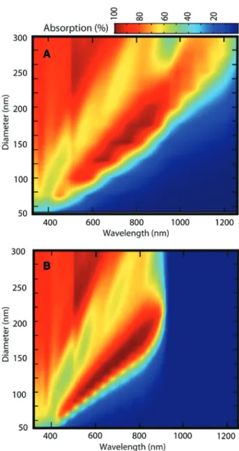
Figure 2: Calculated absorption in NW arrays versus wavelength
and NW diameter at normal incidence.
(A) and (B) show NW arrays with and without embedded DBRs, respectively. The geometrical parameters for both panels are
[36] was chosen to optimize the conditions of good lattice matching to InP for future realization of the solar cells and the requirement of a finite index difference in the DBRs [24]. For the NWs, we chose the diameter D = 200 nm, total length L = 1100 nm (with or without DBRs), and pitch P = 500 nm to make sure that no absorption saturation occurs, which can be observed for longer NWs [9, 10] or denser arrays (smaller pitch) of NWs [6, 8, 12].
Figure 2 shows a comparison between absorption spectra of InP NWs and InGaAs/InP NW-DBRs under normal incidence (θinc = 0°) as a function of D for identical values of P and L. Note that L accounts for the total length of the NWs, including the DBRs. The results indicate two key points: first, the absorption extends to longer wave-lengths by employing DBRs. In particular, the wavelength position of the HE11 mode extends up to about 1150 nm. The extension originates from the absorbing InGaAs layers in the DBRs (see Supplementary Figure S3). Second, the absorption is improved in NW-DBRs in the middle spectral range (500 nm–800 nm for varying D) due to enhanced contributions from the longitudinal Fabry-Perot modes. These longitudinal modes form when the guided modes undergo multiple reflections from the embedded DBRs [8].
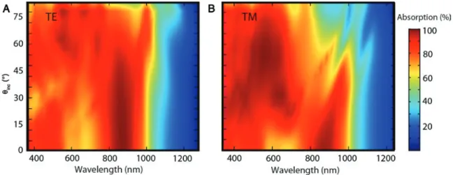
Oblique incident light breaks the symmetry of a NW/ light incidence system and enhances the absorption in the middle part of the solar spectrum by exciting additional Mie resonances [12, 13]. For NWs without DBRs, however, the excitation of symmetry-dependent guided HE1m modes (m is the radial mode number) becomes weaker in both the longest and shortest wavelength parts of the spectrum [12]. By incorporating top and bottom DBRs in the NWs, we can reinforce both the excitation of HE1m modes and Mie resonances and consequently achieve unselective broad-band absorption at certain angles of incidence. Figure 3
below shows TM- and TE-polarized absorption spectra of DBR-NWs versus incident angle θinc. It is readily observed that both polarized spectra exhibit an improved absorp-tion over a broad spectral range at certain incident angles compared to normal incidence absorption.
To clearly compare the absorption enhancement versus θinc, we plot the polarization-averaged absorption spectra of DBR-NWs in Figure 4A. The observed enhancement implies a strong light trapping in the NWs, which effectively reduces the transmission (leakage) of light into the substrate (Figure 4B) while maintaining a more or less constant reflection (not shown). Evidently, the absorption profile around the band gap of InP is significantly broadened upon introducing the InGaAs/InP DBRs, in particular, for θinc ≤ 45° (Figure 4B). To investigate this observation in more detail, we explore sepa-rately the absorption properties of the DBRs and especially the InGaAs layers. Figure 4C shows the absorption spectra versus θinc of the InGaAs layers in the DBRs. A new strong absorption peak at 960 nm is excited, which strongly affects the absorption profile around the band gap energy of InP, leading to the observed broadening effect. Our calculations confirm that the absorption peak at 960 nm stems from rein-forced absorption of the fundamental HE11 mode in the thin InGaAs layers [5] due to multi-reflection from the DBRs. The photon absorption profile for normal incidence at 960 nm, shown in Figure 4D, displays strong light confinement in the InGaAs layers, leading to 390% enhanced absorption from 16% at 800 nm to 78% at 960 nm (Figure 4C). The enhancement at 960 nm can be further boosted up to 83% for oblique incidence at θinc = 30°. The presence of this new strong absorption peak flattens and enhances the absorp-tion spectra of DBR-NWs at long wavelengths ranging from 850 nm to 1000 nm (Figure 4A). Furthermore, calculations show that by increasing the number of DBR periods from 2
Figure 3: Calculated absorption in DBR-NW arrays versus wavelength and angle of incidence.
to 5, the absorption at 960 nm at normal incidence can be enhanced from 78% up to 95% at the expense of slightly more absorbing material. This drastic improvement is due
to a suppressed light transmission from 20% to merely 3% from the DBR-NWs into the substrate while maintaining a constant low reflection of 2% from the NWs.
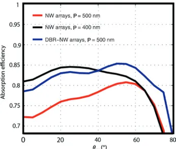
Figure 5 shows the effect of light trapping due to DBRs on the enhancement of the absorption efficiency versus θinc. The results indicate that the absorption efficiency of DBR-NWs with 500-nm pitch (blue trace) exceeds not only that of InP NWs with 400-nm pitch (black trace) for θinc > 40° but also for all angles of incidence for InP NW arrays with 500-nm pitch (red trace).
4 Conclusions
We have theoretically investigated optical absorption in InP NW arrays on InP substrates with integrated In0.56Ga0.44As/InP DBRs inside the wires forming a resonant Fabry-Perot cavity. Detailed calculations show that an unselective 85% light absorption efficiency in the range 300 nm < λ < 920 nm can be achieved in optimized array structures at 50° oblique light incidence. The DBR-NW arrays have the main advantage of small transmission (leakage) of light into the substrate due to strong light
Figure 4: Calculated absorption and transmission in DBR-NW arrays versus wavelength and angle of incidence.
(A) Polarization-averaged absorption spectra versus light incidence angle (θinc) of DBR-NWs. The green trace shows the absorption spectrum
of InP arrays without DBRs under normal incidence. (B) Transmission spectra of DBR-NWs versus θinc. (C) Absorption spectra of the InGaAs
layers as a function of θinc, revealing a strong peak around the band gap wavelength of InP. (D) Photon absorption profile at 960 nm. Inset
shows x-y cross section of photon absorption profile in the middle layer of the top DBR (InGaAs layer).
Figure 5: Calculated absorption efficiency of DBR-NW arrays with
500-nm pitch (blue trace), and for NW arrays without DBRs with 500-nm pitch (red trace) and 400-nm pitch (black trace), respec-tively, versus light incidence angle.
trapping provided by DBRs. The light trapping due to mul-tiple reflections from the DBRs effectively increases the optical path length of the excited modes in the NWs and enhances the absorption efficiency. A key feature underly-ing the significantly enhanced and broadened absorption profile is the appearance of an additional fundamental mode at 960 nm, which leads to both a strong tion in the InGaAs layers and strongly modified absorp-tion properties around the band gap energy of InP. Here we calculated optical spectra for InP NWs, but the results are expected to be valid for other direct band gap III–V semiconductor materials. We believe that our proposed idea of integrating DBRs in NWs offers great potential for new types of high-performance photovoltaic applications. Acknowledgments: This research was supported by Nano-Lund, the Swedish Research Council (VR), the Swedish Foundation for Strategic Research (SSF), and the Knut and Alice Wallenberg Foundation. The authors would like to thank Prof. Mats-Erik Pistol and Dr. Nicklas Anttu for helpful discussions.
References
[1] VJ L, Oh J, Nayak AP, et al. A perspective on nanowire photode-tectors: current status, future challenges, and opportunities. IEEE J Selected Topics Quantum Electron 2011;17:1002–32. [2] Pettersson H, Trägårdh J, Persson AI, Landin L, Hessman D,
Samuelson L. Infrared photodetectors in heterostructure nano-wires. Nano Lett 2006;6:229–32.
[3] Dongdong Y, Tingting H, Qin H, Qianqian L, Yejin Z, Xiaohong Y. High-responsivity 40 Gbit/s InGaAs/InP PIN photodetectors integrated on silicon-on-insulator waveguide circuits. J Semicond 2016;37:1140061–6.
[4] Karimi M, Jain V, Heurlin M, et al. Room-temperature InP/InAsP quantum discs-in-nanowire infrared photodetectors. Nano Lett 2017;17:3356–62.
[5] Lu H, Gang C. Analysis of optical absorption in silicon nanowire arrays for photovoltaic applications. Nano Lett 2007;7:3249–52. [6] Wallentin J, Anttu N, Asoli D, et al. InP nanowire array solar
cells achieving 13.8% efficiency by exceeding the ray optics limit. Science 2013;339:1057–60.
[7] Seo K, Wober M, Steinvurzel P, et al. Multicolored vertical silicon nanowires. Nano Lett 2011;11:1851–6.
[8] Wang B, Leu PW. Tunable and selective resonant absorption in vertical nanowires. Opt Lett 2012;37:3756–8.
[9] Aghaeipour M, Anttu N, Nylund G, Samuelson L, Lehmann S, Pistol ME. Tunable absorption resonances in the ultraviolet for InP nanowire arrays. Opt Express 2014;22:29204–12. [10] Aghaeipour M, Anttu N, Nylund G, Berg A, Lehmann S, Pistol
ME. Optical response of wurtzite and zinc blende gap nanowire arrays. Opt Express 2015;23:30177–87.
[11] Kayes BM, Atwater HA, Lewis NS. Comparison of the device physics principles of planar and radial p-n junction nanorod solar cells. J Appl Phys 2005;97:114302.
[12] Aghaeipour M, Pistol ME, Pettersson H. Considering symmetry properties of InP nanowire/light incidence systems to gain broadband absorption. IEEE Photonics J 2017;9:4501310. [13] Abujetas DR, Paniagua-Domínguez R, Sánchez-Gil JA.
Unrave-ling the Janus role of Mie resonances and leaky/guided modes in semiconductor nanowire absorption for enhanced light harvesting. ACS Photonics 2015;2:921–9.
[14] Kuang P, Eyderman S, Hsieh ML, Post A, John S, Lin SY. Achiev-ing an accurate surface profile of a photonic crystal for near-unity solar absorption in a super thin-film architecture. ACS Nano 2016;10:6116–24.
[15] Muskens OL, Rivas JG, Algra RE, Bakkers EP, Lagendijk A. Design of light scattering in nanowire materials for photovol-taic applications. Nano Lett 2008;8:2638–42.
[16] Van Dam D, van Hoof NJ, Cui Y, et al. High-efficiency nanowire solar cells with omnidirectionally enhanced absorption due to self-aligned indium-tin-oxide Mie scatterers. ACS Nano 2016;10:11414–9.
[17] Fountaine KT, Kendall CG, Atwater HA. Near-unity broadband absorption designs for semiconducting nanowire arrays via localized radial mode excitation. Opt Express 2014;22 Suppl 3:A930–40.
[18] Sturmberg BCP, Dossou KB, Botten LC, et al. Optimizing photovoltaic charge generation of nanowire arrays: a simple semi-analytic approach. ACS Photonics 2014;1:683–9. [19] Fountaine KT, Cheng WH, Bukowsky CR, Atwater HA. Near-unity
unselective absorption in sparse InP nanowire arrays. ACS Photonics 2016;3:1826–32.
[20] Garnett E, Yang P. Light trapping in silicon nanowire solar cells. Nano Lett 2010;10:1082–7.
[21] L. Zeng, Bermel P, Yi Y, et al. Demonstration of enhanced absorption in thin film Si solar cells with textured photonic crystal back reflector. Appl Phys Lett 2008;93:221105.
[22] Zhou D, Biswas R. Photonic crystal enhanced light-trapping in thin film solar cells. J Appl Phys 2008;103:093102. [23] Shen JL, Chang CY, Liu HC, et al. Reflectivity and
photolumi-nescence studies in Bragg reflectors with absorbing layers. Semicond Sci Technol 2001;16:548–52.
[24] Chen L, Towe E. Photonic band gaps in nanowire superlattices. Appl Phys Lett 2005;87:103111.
[25] Svendsen GK, Weman H, Skaar J. Investigations of Bragg reflec-tors in nanowire lasers. J Appl Phys 2012;111:123102.
[26] Glembocki OJ, Piller H. Indium phosphide (InP). In: Palik ED, editor. Handbook of Optical Constants of Solids. Burlington: Academic Press, 1997:503–16.
[27] Kim TJ, Ghong TH, Kim YD, et al. Dielectric functions of InxGa1-xAs alloys. Phys. Rev. B 2003;68:1153231–10.
[28] Accessed October 4, 2017, at http://rredc.nrel.gov/solar/spec-tra/am1.5/.
[29] Fan Z, Kapadia R, Leu PW, et al. Ordered arrays of dual-diam-eter nanopillars for maximized optical absorption. Nano Lett 2010;10:3823–7.
[30] Soucail B, Voisin P, Voos M, Rondi D, Nagle J, de Cremoux B. Optical investigations of the band offsets in an InGaAs-InGaAsP-InP double-step heterostructure. Semicond Sci Technol 1990;5:918–20.
[31] Nahory RE, Pollack MA, Johnston Jr WD, Barns RL. Band gap versus composition and demonstration of Vegard’s law for In 1-xGaxAsyP1-y lattice matched to InP. Appl Phys Lett 1978;33:659–61.
[32] Furtado MT, Loural MSS, Sachs AC, Shieh PJ. Band offset in GaAlAs and InGaAs: InP heterojunctions by electro chemical CV profiling. Superlattices Microstruct 1989;5:507–10. [33] Grzela G, Paniagua-Domínguez R, Barten T, van Dam D,
Sánchez-Gil JA, Rivas JG. Nanowire antenna absorption probed with time-reversed fourier microscopy. Nano Lett 2014;14:3227–34.
[34] Zhang X, Sun XH, Huang H, Wang X, Huang Y, Ren X. Optical absorption in InP/InGaAs/InP double-heterostructure nanopillar arrays for solar cells. Appl Phys Lett 2014;104:0611101–5.
[35] Wilt DM, Fatemi NS, Hoffman Jr RW, et al. High efficiency indium gallium arsenide photovoltaic devices for thermophotovoltaic power systems. Appl Phys Lett 1994;64:2415–7.
[36] Lee CD, Forrest SR. Effects of lattice mismatch on InxGa1-xAs/ InP heterojunctions. Appl Phys Lett 1990;57:469–71.
Supplemental Material: The online version of this article offers