Abstract
Electronics today rely heavily on silicon transistors which are unsuitable for extreme environments where temperatures potentially could reach up to 500◦C. Materials other than silicon has been proposed to solve this problem, one of which is silicon carbide. Transistors made of silicon carbide can with-stand higher temperatures than its silicon counterparts and could potentially be used for exploring hostile planets such as Venus or in high temperature applications such as sensors for engines.
This project is a part of KTHs student satellite initiative which will send a satellite into orbit containing several experiments. One of the experiments is the SiC in space project which is described in this thesis and is largely based on previous works in this particular project.
The goal for this thesis is to ensure that the SiC in space experiment is ready for launch into orbit. This was done by conducting tests in differ-ent temperatures as well as developing software for analyzing data from the experiment as well as modifying already existing software. Based on these tests, it is concluded that the silicon carbide transistors behaves in an ex-pected way and that the platform which operates the experiment is capable of withstanding temperatures up to 100◦C. If the satellite survives launch it is most likely that the data generated by the SiC in space project will be of use for determining the suitability of silicon carbide for space applications. Keywords
Sammanfattning
Elektronik idag f¨orlitar sig p˚a kiseltransistorer som ¨ar ol¨ampliga f¨or extrema milj¨oer d¨ar temperaturer kan n˚a upp till 500◦C. Andra material ¨an kisel har f¨oreslagits f¨or att l¨osa detta problem, d¨ar kiselkarbid ¨ar en av dem. Transis-torer gjorda av kiselkarbid klarar av h¨ogre temperaturer ¨an kiseltransistorer och kan potentiellt anv¨andas f¨or utforskning av planeter med extrema klimat eller f¨or applikationer vid h¨oga temperaturer s˚a som sensorer inne i motorer. Detta projekt ¨ar en del av KTHs student satellit som kommer s¨andas ut i omloppsbana runt jorden b¨arandes p˚a ett antal olika experiment, d¨aribland dem finns ”SiC in space” projektet som beskrivs i denna uppsats.
M˚alet med arbetet i denna rapport ¨ar att s¨akerst¨alla att ”SiC in space” experimentet ¨ar redo f¨or uppskjutning till rymden. Detta gjordes genom att testa vid olika temperaturer och genom att utveckla mjukvara f¨or analyser-ing av experimentdata samt genom sm˚a modifieringar av mjukvara skriven i tidigare arbeten. Baserat p˚a de tester som har genomf¨orts dras slutsatsen att kiselkarbidtransistorn har en acceptabel karakt¨aristik och att plattformen som k¨or experimentet klarar av temperaturer upp till 100◦C. Om satelliten ¨
overlever uppskjutning ut i rymden kommer med st¨orsta sannolikhet ex-perimentet att fungera som ¨onskat och generera data som kan p˚avisa ifall kiselkarbid ¨ar l¨ampligt f¨or applikationer i rymden.
Table of Contents
1 Introduction 1 1.1 Background . . . 1 1.2 Problem description . . . 1 1.3 Purpose . . . 2 1.4 Goal . . . 21.5 Benefits, Ethics and Sustainability . . . 2
1.6 Delimitation . . . 3
1.7 Methodology . . . 3
1.8 Outline . . . 3
2 Background - SiC in space 5 2.1 MIST . . . 5
2.2 Suitability of SiC . . . 5
2.3 Previous works - SiC in space . . . 5
2.4 MIST Space Protocol . . . 6
2.5 Testing of PCB . . . 6
2.6 BJT - Bipolar Junction Transistor . . . 7
3 Method 9 3.1 Literature study . . . 9 3.2 SiC PCB . . . 9 3.3 Working method . . . 9 3.4 Documentation . . . 9 4 Measurements 11 4.1 Calculating current gain . . . 11
4.2 Physical implementation - Measurement circuit . . . 12
4.3 Measuring temperature . . . 13 5 Hardware 15 5.1 Assembly . . . 15 5.1.1 ESD . . . 15 5.1.2 Contamination . . . 15 5.1.3 Preparations . . . 15 5.1.4 Solder tools . . . 16 5.2 Temperature tolerance . . . 16 5.3 Circuit blocks . . . 17 5.4 Temperature sensors . . . 19 5.5 SiC BJT . . . 20
6 Software for SiC PCB 21 6.1 Tools . . . 21 6.2 Communication . . . 21 6.2.1 MSP opcodes . . . 21 6.2.2 I2C . . . . 21 6.2.3 RS-485 - Piezo LEGS . . . 22 6.3 Test driver . . . 22 6.4 Software modifications . . . 23 6.5 Core loop . . . 24 6.6 Experiment driver . . . 25 6.7 UML diagrams . . . 29
7 Data graphing tool 31 7.1 Data format . . . 31
7.2 Configuration file . . . 31
8 Testing 33 8.1 Tools used when testing . . . 33
8.2 Hardware verification . . . 33 8.3 Expected results . . . 34 9 Results 35 9.1 Graphs . . . 35 9.2 Temperature shift . . . 36 10 Evaluation 37 10.1 Current gain beta . . . 37
10.2 Diode characteristics . . . 37
10.3 Conclusion . . . 38
11 Future work 39
A Bill of materials 43
B Temperature Look up table 45
C On-Board computer emulator config 48
D Testing procedure 50
E Graphing tool - configuration file 54
F Github 56
G MCU pin-out 57
H Bigger graphs 58
H.1 Beta . . . 58 H.2 Ube, Ib . . . 60
List of Figures
1 BJT symbol . . . 7
2 Measurement circuit for Ub and Uc . . . 12
3 Sub-circuits on PCB . . . 17
4 SiC PCB connectors . . . 18
5 Die with array of SiC BJTs . . . 20
6 Main loop flowchart . . . 24
7 SiC experiment flowchart . . . 26
8 UML Piezo . . . 29
9 UML diagram SiC . . . 30
10 BJT characteristic Ube curve . . . 34
11 BJT characteristic Beta curve Si . . . 34
12 Analyzed and filtered data. . . 35
13 SiC Ib/Ube . . . 38 14 Si Beta . . . 58 15 SiC β/Ic . . . 59 16 Si Ib/Ube . . . 60 17 SiC Ib/Ube . . . 61
List of Tables
1 List of components and temperature tolerances . . . 162 SiC PCB, pin-out for LEGS section . . . 18
3 SiC PCB, Pin-out Seud . . . 19
4 SiC PCB, pin-out for Cubes section . . . 19
5 MSP opcodes for Sic in Space and Piezo LEGS. . . 22
6 ASCII commands used for Piezo Legs . . . 22
7 SiC experiment data buffer . . . 27
8 Structure of CSV, with the proper header descriptors . . . 31
9 Units of each data field . . . 31
10 Configuration settings for graphing tool . . . 32
11 Average Ube shift over measured temperatures . . . 36
List of abbreviations
MIST MIniature Student saTellite SiC Silicon Carbide
BJT Bipolar Junction Transistor
LEO Low Earth Orbit
PCB Printed Circuit Board
MSP MIST space protocol
OBC On-Board computer
ESD Electrostatic Discharge
LUT Look up table
CSV Comma Seperated Values
MCU Microcontroller Unit
SWD Serial Wire Debug
1
Introduction
This thesis is based on and a continuation of previous works on the SiC in space KTH MIniature STudent satellite (MIST) project. The aim for this thesis is to test the design and correct the design where possible.
1.1
Background
MIST is a project organized by KTH Space Center [1] which gives students the opportunity to take part in the development a satellite. The experiments which will be carried by MIST are as follows[2].
• CubeProp, Propulsion experiment
• RATEX-J, testing of key components for mass spectrometer • Piezo LEGS, testing of linear piezoelectric motor
• CUBES, X-ray Background Explorer
• SiC in space, testing of integrated circuit made of silicon carbide • MoreBac, resuscitation of lyophilized microorganisms
• SEUD, testing of correcting faults in memory due to radiation Descriptions for each project can be found on the MIST website[3]. SiC in space - Working on Venus
Working on Venus is a project that aims to develop silicon carbide (SiC) devices and integrated circuits that can withstand the harsh environment on Venus [4, 5].
The SiC in space project aims to send a bipolar junction transistor (BJT) made of SiC into low earth orbit(LEO) in order to test if the technology works in space. If the tests are successful the SiC BJT might be used in a future probe that will be sent to Venus.
1.2
Problem description
This thesis will cover these four tasks:
1. Assemble and test the final PCB(Printed Circuit Board) in different temperatures up to 100◦C to ensure that the PCB does not have any unexpected break downs.
2. Update code to support the PCB handled in this work. The latest work were done on version 3 of the system, this work will focus on version 4. 3. Write a program for analyzing the data generated by the PCB.
4. Document code and hardware for handing over the PCB to the MIST team, or the next group that will work on this project.
1.3
Purpose
The purpose of this thesis is to document the testing of the complete PCB, including software and hardware, and establishing documentation for the PCB and its final code. The documentation of software will help with future projects should the need arise.
1.4
Goal
The goal of this project is to ensure that the final version of the PCB is ca-pable of withstanding the temperature that it will be subjected to in space. The PCB needs to be tested in different temperatures to determine if the components can withstand the temperature in space. Earlier works has cre-ated a testing procedure for testing the different components, which needs to be extended for the final version.
Along side with the goal of this project is the overarching goal present in all previous works with the purpose of collecting data about the behavior of a SiC BJT and the Piezo motor in space.
1.5
Benefits, Ethics and Sustainability
It is currently known that SiC components can withstand higher tempera-tures than regular Si which makes SiC a suitable material when designing high temperature environments[6, p. 6]. The SiC in space experiment could provide valuable information about SiC BJTs and their capabilities in space. A big problem with sending satellites into space is space debris. It is cur-rently feasible to send satellites into space with low risk of losing the satellite to space debris. In order to prevent producing more space debris, which could potentially lead to an unsafe environment for satellites, the satellite in this project will burn up in the atmosphere once the experiments are com-plete. Should this fail however, there is a possibility that the MIST project creates more space debris which could potentially destroy future satellites or spacecraft [7, 8, 9].
1.6
Delimitation
This project is limited to testing version 4 of the PCB for the SiC and Piezo LEGS experiments, this includes writing/modifying already existing code to work with version 4. The modifications to the PCB were made by Bengt Molin.
Software for analyzing the data generated by the SiC experiment will be made. Analysis for the Piezo LEGS or any other experiment sent with the SiC experiment into space will not be included in this project. Gathering of data and the subsequent organizing will not be part of this project either, attempts will however be made to make the organization of data simple.
1.7
Methodology
The nature of this project is to gather and solidify data from previous works as well as testing the PCB to ensure that it works. For this, a qualitative research has been conducted where the previous works has been read and analyzed in order to understand the structure of the software and the hard-ware.
An empirical study has been used for testing the PCB to ensure the integrity of the hardware and software.
1.8
Outline
Chapter 2 explains some of the background for this project and brings up some of the necessary information used in this project.
Chapter 3 describes the methodology behind this project.
Chapter 4 describes how measurements will be taken in the experiment as well as describing the calculations used in the project.
Chapter 5 describes the hardware in this project as well as the procedure used during the assembly of the PCB.
Chapter 6 describes the software used to control the two experiments. Chapter 7 describes the tool developed for viewing data generated by the SiC in space project.
Chapter 9 contains the results from the testing. Chapter 10 discusses the results.
Chapter 11 discusses tasks that could be worked on by future groups.
2
Background - SiC in space
SiC in space is part of a project organized by the MIST team and is one of seven experiments that will be sent into a lower Earth orbit. The satellite that will be used is a CubeSat, which is a very small satellite designed by California Polytechnic State University, San Luis Obispo and Stanford Uni-versity’s Space Systems Development Lab to make it easier for students to launch experiments into space[10].
2.1
MIST
The MIST project, led by Dr (h.c.) Sven Granh, is a project that sev-eral groups of students has worked on since 2015 where the experiments are handed over to new groups of students after every semester with the goal of eventually getting the experiments ready for space.
2.2
Suitability of SiC
The environment aimed for with SiC are high-temperature climates, or for this project, the surface of Venus which is approximately 470◦C[11]. It has been shown that components made of SiC can withstand this temperature[5]. Apart from working on other planets, SiC transistors could potentially be used for applications located in high temperature places such as a sensor in an engine.
This experiment tries to determine the suitability for SiC in space. If this experiment is successful, SiC electrical components could possibly be sent to Venus.
2.3
Previous works - SiC in space
The SiC in space project has been worked on for a few years with a number of different groups of students which are listed below.
• Design of measurement circuits for SiC experiment[12]
• Design of microcontroller circuit and measurement software for SiC and MOREBAC experiment[13]
• Design of power supplies for Piezo LEGS and SiC experiment[14] • Design and test of SiC circuit board for MIST satellite[15]
• Embedded programming and construction of the PCB SiC In Space experiment[16]
• Implementation of the communication between SiC, Piezo-LEGS and On-board Computer[17]
The main focus of this thesis revolves around testing and evaluating the work done in [16] and [17].
2.4
MIST Space Protocol
The MIST team has developed a protocol called MSP(MIST Space Protocol) which is built on I2C and is used to handle all communications with the OBC. The protocol specifies what kind of information will be sent and in what order.
MSP uses a transfer speed of 400 kbit/s, also known as ”fast mode” in I2C .
2.5
Testing of PCB
The protocol for testing the board was created by D. Rosenkvist and J. Eriksson and focuses on the function of the components and verifying the electrical characteristics of both the SiC BJT and the Si BJT.
A tool to process the raw data from the PCB was written for testing purposes which includes visual representation of the processed data in graphs.
2.6
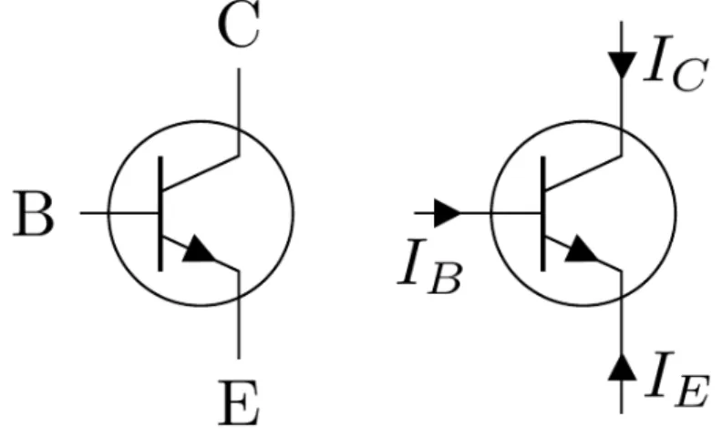
BJT - Bipolar Junction Transistor
A BJT is a type of transistor that is controlled by currents rather than voltages. The base current controls the current flow from collector to emitter. Normal applications for a BJT could be in switches as well as being used for amplification of currents.
Figure 1: BJT symbol and current paths.
Figure 1 shows the direction of currents in relation to the transistor where B is the base, C the collector and E the emitter.
3
Method
A literature study was conducted studying previous works in the project, since it was the resulting products of these works that was under testing for the work described in this thesis.
3.1
Literature study
This project is a continuation of previous works within the SiC in space project and in order to understand the current state of the project, all pre-vious works regarding the SiC in space and Piezo Legs were read. Most of the focus were on the latest two works due to relevance to this project where the latest works described the current state of the software and the different parts of the PCB and its design in its most up-to-date form.
The MSP was studied in order to understand the underlying work that had been implemented in the project for communication between the OBC(On-board Computer) and SiC in space.
3.2
SiC PCB
With each iteration of hardware tests must be conducted to ensure that any defects are discovered and corrected. For this, software were developed to specifically allow for testing without the need for the OBC to provide instructions in order to simplify the testing procedure.
3.3
Working method
The software used for the experiment PCB was developed using an iterative approach since the majority of the code was already written and only needed small changes to function properly.
Software for the graphing tool was developed using test driven develop-ment. This approach was deemed to be good enough for the lightweight tool that was created. Using this has the advantage of compartmentalizing the code and making sure that any changes made does not break the code in other places.
3.4
Documentation
In order for this project to be useful to others, it is important that it is doc-umented properly. However, the different parts for the SiC in space project has already been documented in the works that designed the parts. Instead
of documenting these parts again, the documentation for this project was written for ease of implementation and access to the basics of how the SiC PCB operates.
4
Measurements
The MCU can only measure voltage levels with its ADC, due to this we have to calculate the desired measurements from these voltages.
The circuit used for this experiment uses instrumentation amplifiers in order to measure the voltage used to determine the currents Ib and Ic for each of the transistors. The temperature is measured with sensors mounted on the PCB.
4.1
Calculating current gain
The current gain β is calculated with the formula β = Ic
Ib. The currents Icand Ib is derived by measuring the voltage drop over resistors placed in series with the base and collector respectively for each BJT. Each side of the resistor is connected to an instrumentation amplifier which feeds the difference in voltage to an ADC. The instrumentation amplifier has a high resistance on its inputs preventing it from drawing too much of the current itself allowing us to simplify the equations. Using Ohm’s law it is possible to calculate the current
U = R ∗ I (1)
I = U
R (2)
Where the voltage drop is calculated as
U = U1− U2 (3)
R is the resistance, I the current and U the voltage. Combining equations 3 and 2 we get the formula
I = U1− U2
R (4)
We can determine the function for calculating current gain from the volt-ages by combining equation 4 with the formula for current gain 5.
β = Ic Ib (5) β = U1c−U2c Rc U1b−U2b Rb (6)
β = Rb∗ (U1c− U2c) Rc∗ (U1b− U2b) (7) β = Rb Rc ∗ U1c− U2c U1b− U2b (8) β = Rb Rc ∗ Uc Ub (9)
4.2
Physical implementation - Measurement circuit
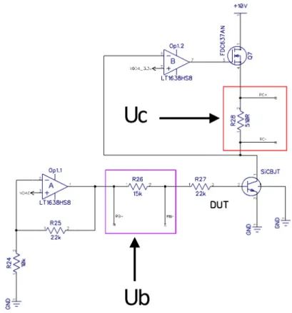
Figure 2: Measurement circuit for Ub and Uc
Figure 2 shows how the function to calculate current gain is implemented on the SiC PCB. The formula for calculating the current gain is in this case
β = R26 R28 ∗ URC+− URC− URB+− URB− (10) β = 15000 510 ∗ Uc Ub (11) 12
4.3
Measuring temperature
The temperature sensors output a voltage level in the range of 301 to 1955 mV which can be translated into Celsius with a LUT(Look-Up table) or calculated directly from the formula [18].
T = 8.194 −p(−8.192)
2 + 4 ∗ 0.00262 ∗ (1324 − mV )
2 ∗ −0.00262 + 30 (12)
5
Hardware
The PCB used in this project is a slightly modified PCB from previous works and is version 4 of the SiC PCBs. Changes made to version 3 includes adding an additional signal line for the RS-485 circuit which makes it possible to turn off the communication with Piezo-LEGS when it is not in use, and repositioning as well as changing the type of some of the Molex connectors.
5.1
Assembly
Since version 4 is the current candidate for launch into space, some precau-tions were taken to mitigate damage and contamination of the PCB during assembly and handling when testing the PCB.
5.1.1 ESD
ESD(Electrostatic Discharge) can cause damage to electrical components. If a discharge occurs it can be difficult to determine the full extent of the dam-age caused by it. If ESD has occured, a component might not look damdam-aged and could potentially function for a while, but with a severe reduction on its lifetime [19].
In order to mitigate ESD, all sensitive equipment and all electrical com-ponents as well as the PCB were placed on an ESD-mat in addition to using an ESD-bracelet at all times while handling the components and PCB. These precautions, however, does not guarantee that the PCB and its components was not exposed to ESD.
5.1.2 Contamination
Contamination of the PCB could cause problems in a vacuum when fat from fingers or moisture is present on the PCB. In order to mitigate this, gloves were used to prevent fat from fingers when handling the card. Isopropyl alcohol was used to clean the tools used during assembly and the PCB where needed.
5.1.3 Preparations
The steps taken 1. Put on gloves
3. Clean tools with isopropyl alcohol 4. Place tools on ESD-mat
5.1.4 Solder tools
The PCB was assembled using a hot air gun at 270◦C and a heating bed set to 230◦C. Lead-free solder was used during assembly.
5.2
Temperature tolerance
All components were chosen in order to withstand higher temperatures where possible whilst only considering commercially available products.
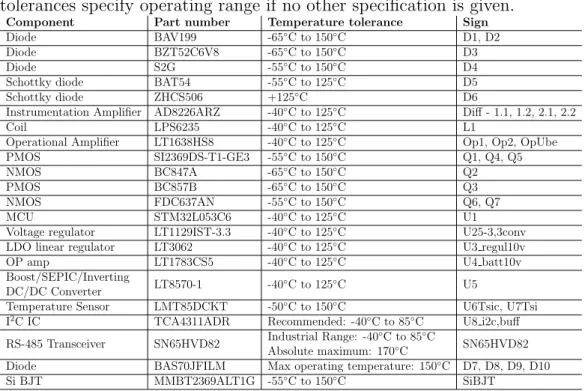
Table 1: List of components with respective temperature tolerances. All tolerances specify operating range if no other specification is given.
Component Part number Temperature tolerance Sign
Diode BAV199 -65◦C to 150◦C D1, D2
Diode BZT52C6V8 -65◦C to 150◦C D3
Diode S2G -55◦C to 150◦C D4
Schottky diode BAT54 -55◦C to 125◦C D5
Schottky diode ZHCS506 +125◦C D6
Instrumentation Amplifier AD8226ARZ -40◦C to 125◦C Diff - 1.1, 1.2, 2.1, 2.2
Coil LPS6235 -40◦C to 125◦C L1
Operational Amplifier LT1638HS8 -40◦C to 125◦C Op1, Op2, OpUbe
PMOS SI2369DS-T1-GE3 -55◦C to 150◦C Q1, Q4, Q5
NMOS BC847A -65◦C to 150◦C Q2
PMOS BC857B -65◦C to 150◦C Q3
NMOS FDC637AN -55◦C to 150◦C Q6, Q7
MCU STM32L053C6 -40◦C to 125◦C U1
Voltage regulator LT1129IST-3.3 -40◦C to 125◦C U25-3,3conv
LDO linear regulator LT3062 -40◦C to 125◦C U3 regul10v
OP amp LT1783CS5 -40◦C to 125◦C U4 batt10v
Boost/SEPIC/Inverting
DC/DC Converter LT8570-1 -40
◦C to 125◦C U5
Temperature Sensor LMT85DCKT -50◦C to 150◦C U6Tsic, U7Tsi
I2C IC TCA4311ADR Recommended: -40◦C to 85◦C U8 i2c,buff
RS-485 Transceiver SN65HVD82 Industrial Range: -40
◦C to 85◦C
Absolute maximum: 170◦C SN65HVD82
Diode BAS70JFILM Max operating temperature: 150◦C D7, D8, D9, D10
Si BJT MMBT2369ALT1G -55◦C to 150◦C SiBJT
5.3
Circuit blocks
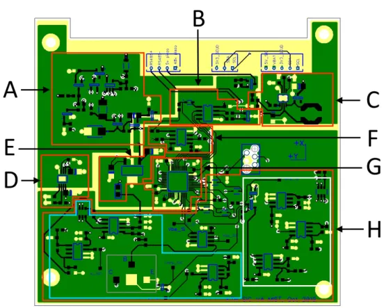
Figure 3: Sub-circuits on PCB
Each block in figure 3 represents the physical placement of the sub-circuits.
A Battery Bus Power Switch with an inrush current protection circuit B RS-485 Transceiver
C 48V Piezo LEGS DC-DC Boost converter D 10V Linear converter
E 3.3V Linear converter F I2C Buffer
G MCU
• White: Si specific circuit • Teal: SiC specific circuit Connectors
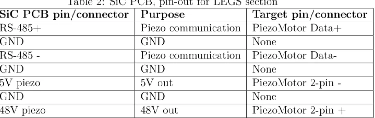
These tables correspond to the physical placement of each pin, where the first pin to the left of each connector is the first pin in each table.
Figure 4: SiC PCB connectors
Table 2: SiC PCB, pin-out for LEGS section
SiC PCB pin/connector Purpose Target pin/connector
RS-485+ Piezo communication PiezoMotor Data+
GND GND None
RS-485 - Piezo communication PiezoMotor
Data-GND GND None
5V piezo 5V out PiezoMotor 2pin
-GND GND None
48V piezo 48V out PiezoMotor 2-pin +
Table 3: SiC PCB, pin-out for Seud section. The text on the PCB for SDA is slightly misaligned. The correct pin is as shown in the table.
SiC PCB pin/connector Purpose Target pin/connector
3V3 seud ? None
GND GND None
SDA I2C OBC or SDA 20 on DUE
GND GND None
SCL I2C OBC or SCL 21 on DUE
Table 4: SiC PCB, pin-out for Cubes section
SiC PCB pin/connector Purpose Target pin/connector
5V SiC 5V in Power supply
GND GND None
VBAT 14V in Power supply
GND GND None
3V3 SEUD ? Not connected to SiC
GND GND None
SDA I2C OBC or SDA 20 on DUE
GND GND None
SCL I2C OBC or SCL 21 on DUE
5.4
Temperature sensors
Two temperature sensors are used to measure the temperature of each BJT. The grounds on the two respective BJTs are connected to their separate temperature sensors creating a path for the heat to transfer over to the sensors. The SiC BJT is not bonded to the large ground pad but instead glued onto the pad, which should not affect to temperature transfer too much but it is worth keeping in mind that the results might not be as expected due to this. It is important to note that the temperature sensors have a typical accuracy of ±0.4◦C but can vary up to ±2.7◦C in a worst case scenario.
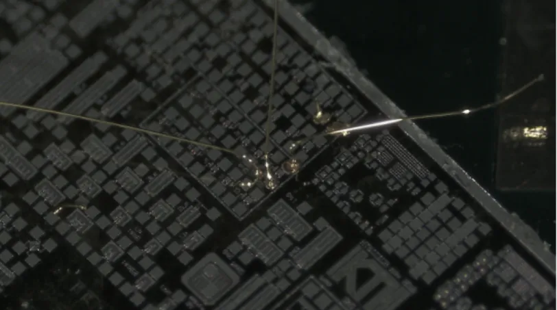
5.5
SiC BJT
The SiC BJT is an experimental BJT from KTH and is attached to an array of SiC BJTs on a small die. There is no package to protect the bonds from breaking and care needs to be taken with the PCB to prevent detachment of the bonding wires.
Figure 5: Die with array of SiC BJTs
6
Software for SiC PCB
The code used in this project for controlling the MCU, running the experi-ments and handling communications of both I2C and RS-485 was written in previous works with a small modification to the RS-485 protocol along side creating a test driver to run tests on the PCB and some minor changes to the code.
For an in-depth look of how the code works, it is recommended to read the previous works [16, 17].
Software written for the SiC PCB was made following the requirements from the MIST team such as implementing MSP and the capability to turn off power to the experiment sub-circuits.
6.1
Tools
All software was written in IAR Embedded Workbench and uses the HAL library. CubeMX was used to generate the initialization code for the MCU. The development board STM32F3DISCOVERY was used to program the MCU over SWD(Serial Wire Debug) as well as debugging and retrieving data.
6.2
Communication
MSP is implemented for SiC in space and Piezo LEGS, where the SiC in space MCU handles all communications with the OBC and acts as a middleman for Piezo LEGS.
6.2.1 MSP opcodes
Commands created for both the SiC experiment and Piezo LEGS utilizes the same pattern as specified by MSP with 0x5X as system commands and 0x6X as requests.
6.2.2 I2C
The implementation of I2C utilizes an interrupt-based system making it pos-sible to communicate with the SiC in space MCU when needed. However, this also brings the risk of interrupting the experiment or task being per-formed. As mentioned in 2.4, the OBC has a transfer rate of 400 kbit/s but the current implementation of I2C in the SiC in space project is only capa-ble of 100 kbit/s. This remains unsolved since the reason of this procapa-blem is unknown.
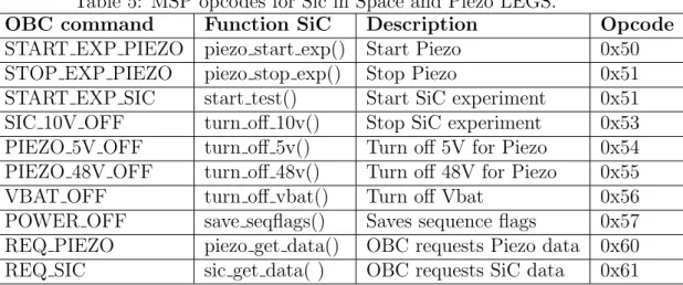
Table 5: MSP opcodes for Sic in Space and Piezo LEGS.
OBC command Function SiC Description Opcode
START EXP PIEZO piezo start exp() Start Piezo 0x50
STOP EXP PIEZO piezo stop exp() Stop Piezo 0x51
START EXP SIC start test() Start SiC experiment 0x51
SIC 10V OFF turn off 10v() Stop SiC experiment 0x53
PIEZO 5V OFF turn off 5v() Turn off 5V for Piezo 0x54
PIEZO 48V OFF turn off 48v() Turn off 48V for Piezo 0x55
VBAT OFF turn off vbat() Turn off Vbat 0x56
POWER OFF save seqflags() Saves sequence flags 0x57
REQ PIEZO piezo get data() OBC requests Piezo data 0x60
REQ SIC sic get data( ) OBC requests SiC data 0x61
6.2.3 RS-485 - Piezo LEGS
Communication between the SiC in space MCU and Piezo LEGS is handled using the protocol RS-485 and is implemented with a RS-485 transceiver SN65HVD82. UART is used to communicate Between the SiC in space MCU and the RS-485 transceiver.
All data sent between Piezo LEGS and the SiC PCB is in ASCII char-acters and uses simple commands to specify the desired operation of Piezo LEGS similar to MSP opcodes.
Table 6: ASCII commands used for Piezo Legs
Command Function
XM3 Start experiment
XM4 Stop experiment
XU6 Collect data
6.3
Test driver
The test driver developed in this project was made to act as if a command has been sent by the OBC and consists of a few tests that turns the two experiments on and off as well as testing the voltage regulators.
The test driver does not test communication with the OBC and instead focuses on the functionality of the PCB itself, but it does attempt to com-municate with Piezo LEGS and retrieve data from it ensuring that the whole package of SiC in space and Piezo LEGS will behave in a reasonable way.
6.4
Software modifications
The ADC was previously set to a sampling time of 1.5 cycles which was too short to be able to measure any of its channels. Using a sampling rate of at least 12.5 cycles should provide enough time to sample each channel. In addition to this change, the number of samples taken for a data point was increased to 16 samples instead of 1 sample. This did not have a pronounced effect on the results, only increasing the accuracy of the ADC with a few units. Considering that the ADC has 12 bits of resolution and a few units can in this case be defined as 4 units for simplicity, the total gain in accuracy lies somewhere around 40954 . However, in the event of a spike due to radiation or any other unexpected cause, this sampling might provide some stability to the results and is for this reason kept rather than dismissed.
6.5
Core loop
Figure 6: Main loop flowchart. Slightly modified from [17, p. 23].
Implementation
The core loop is implemented with a short infinite while loop which waits for I2C communication before proceeding with any calculations or measure-ments.
1 i f( HAL I2C Slave TxRx IT(& h i 2 c 1 , ( u i n t 8 t ∗ ) a B u f f e r , b u f f L e n g t h ) != HAL OK) 2 { 3 E r r o r H a n d l e r ( ) ; 4 } 5 6 // w a i t f o r t h e i 2 c r e c e p t i o n t o f i n i s h t h i s must t i m e o u t a t some p o i n t , o t h e r w i s e t h e r e i s r i s k f o r g e t t i n g s t u c k .
7 w h i l e ( HAL I2C GetState(& h i 2 c 1 ) != HAL I2C STATE READY) 8 {
9 10 }
Whatever command that has been sent during communication will be executed if the transferdirection is set to 0, otherwise a callback is called.
1 i f ( ! t r a n s f e r D i r e c t i o n G l o b a l )// i f we r e c i v e d a command 2 { 3 // t h i s f u n t i o n r e t u r n e s t h e n e g a t i v e e r r o r c o d e s i n MSP. 4 m s p r e c v c a l l b a c k ( ( u i n t 8 t ∗ ) a B u f f e r , b u f f L e n g t h , addr ) ; 5 m s p s e n d c a l l b a c k ( ( u i n t 8 t ∗ ) a B u f f e r , &b u f f L e n g t h , addr ) ; 6 7 /∗ t h i s t e l l s us i f we a r e i n a msp t r a n s a k t i o n , e x c e p t f o r t h e t i m e i n b e t w e e n t h e msp c o d e i s r u n n i n g 8 and t h e i 2 c c o d e i s r u n n i n g , n e e d s t o be c o v e r e d by f l o w c o n t r o l l ∗/ 9 } 10 e l s e // i f a command was s e n t 11 { 12 F l u s h B u f f e r 8 ( ( u i n t 8 t ∗ ) a B u f f e r , b u f f L e n g t h ) ; 13 i f( m s p e x p s t a t e . t y p e == MSP EXP STATE READY &&
h a s f u n c t i o n t o e x e c u t e ) 14 { 15 ( ∗ command ptr ) ( ) ; 16 h a s f u n c t i o n t o e x e c u t e = f a l s e ; 17 } 18 } 19
If a command has been received from the OBC, the pointer command ptr is set to the desired method and then executed.
6.6
Experiment driver
The main bulk of the experiment driver was written by H. Hatemipur and operates by simply adjusting the voltage level over the base resistors of the
BJTs with a DAC(Digital-to-Analog Converter) and then reading the voltage drop using an ADC measuring the voltage as specified in 4.2.
Figure 7: SiC experiment flowchart 26
The driver saves the result from the ADC through a custom struct and takes 90 samples for each transistor at different base voltages by setting the DAC to 90 different voltage steps in the range of 300 mV to 3000 mV.
1 s t r u c t e x p e r i m e n t p a c k a g e { 2 u i n t 1 6 t t e m p e r a t u r e ;
3 u i n t 1 6 t Vbe ; // v o l t a g e drop from b a s e t o e m i t t e r 4 u i n t 1 6 t Vb ; // v o l t a g e o v e r r e s i s t o r on b a s e 5 u i n t 1 6 t Vc ; // v o l t a g e o v e r r e s i s t o r on c o l l e c t o r 6 } ;
It was found that the experiment package does not clear any residual data if the MCU is not rebooted, causing faulty data to lie in the memory. This was changed to allow for multiple experiments on a single boot-cycle by clearing the data after every experiment cycle.
Experiment data
Data generated from the experiment is saved in a buffer containing 64 un-signed bytes, 2 bytes for each data point since the data points are stored as unsigned 16 bit values. This is done to be able to send data over I2C which works by sending 1 byte at a time. Due to this, each data point needs to be restored once received either by the OBC or on ground. Table 7 shows the byte sequence in which the data is sent to the OBC.
Table 7: SiC experiment data buffer
Byte Data BJT Byte Data BJT Byte Data BJT
0 Temp Si 6 Uc Si 12 Ub SiC
1 Temp Si 7 Uc Si 13 Ub SiC
2 Ube Si 8 Temp SiC 14 Uc SiC
3 Ube Si 9 Temp SiC 15 Uc SiC
4 Ub Si 10 Ube SiC
5 Ub Si 11 Ube SiC
The sequence to restore the data could look like this.
1 t e m p e r a t u r e r e c o n s t r u c t e d = ( d a t a [ 0 ] << 8 ) + d a t a [ 1 ] ; 2 u b e r e c o n s t r u c t e d = ( d a t a [ 2 ] << 8 ) + d a t a [ 3 ] ; 3 u b r e c o n s t r u c t e d = ( d a t a [ 4 ] << 8 ) + d a t a [ 5 ] ; 4 u c r e c o n s t r u c t e d = ( d a t a [ 6 ] << 8 ) + d a t a [ 7 ] ;
The way the data has been disassembled is by shifting the highest byte one byte lower.
And then placing the lower byte into the buffer after the previous byte.
1 b u f f e r [ i +1]= e x p e r i m e n t s [ y ] . t e m p e r a t u r e & 0xFF ;
6.7
UML diagrams
UML diagrams for the operation of both experiments were made in a pre-vious work by S. Lagerqvist and D. Ghaderi but is presented here to make it accessible. These diagrams describes the desired communication pattern from the OBC regarding both Piezo LEGS and the SiC in space project. Operation procedure for the SiC in space project has been slightly modified and requires more time to complete a full run of the experiment. [17].
Figure 9: UML diagram for SiC experiment
7
Data graphing tool
The software developed in this project aims to visually represent the data gathered by the SiC experiment and is written in python 3 with the packages matplotlib and scipy. The tool can generate graphs from data as well as provide fitted equations simplifying the process of analyzing the data.
Data is read from a file called ”data.csv” by default and can be changed through a configuration file called ”config” along side with a few other com-mands. Data generated by the tool will be saved in a csv file with the delimiter set to ”;”.
7.1
Data format
Data is stored in a CSV(Comma Separated Values). The order of data is not important as long as the header contains the proper descriptions of each column. When the program parses the CSV it will try to organize the data in each header into two different tables based on the keywords ”sic” and ”si”.
Table 8: Structure of CSV, with the proper header descriptors
time sic ube sic uc sic ub sic temp si ube si ub si uc si temp
2019-12-23 13:34 2000 9000 3000 1176 700 9000 4000 1423
2019-12-23 14:34 2000 1000 8000 659 700 3000 10000 579
2019-12-23 15:34 2000 2000 6000 1936 700 5000 1000 623
Table 9: Units of each data field
Header(s) Data unit
time Year-Month-Day Hour:Minute
ube, uc, ub [mV]
temp [mV] or [◦C]
The format of the data needs to be either an integer, hexadecimal value or float. If floats are used, it is important that there is no hexadecimal value in the data. As an example, table 8 contains floats and integers forcing the definition of the data format to be specified as floats. Table 9 shows the physical unit used for each data field.
All data can be in either ADC values or regular values.
7.2
Configuration file
The configuration file is used by the tool to determine the data format of the data and the graph settings as well as determining the value of the resistors
used to calculate current gain. The available settings that can be changed are showed in table 10.
Table 10: Configuration settings for graphing tool
Setting Description
Filename The file where data is stored
si rb, si rc, sic rb, sic rc Resistor value for electrical current calculation sic color, si color Sets the color of the graphs
dotted Set if the data points should be added to the graph
lines Set if a line should be drawn between data points
graph type Sets the graph type to display
fit function Specifies the function for the fitting the data
x axis Determine what unit the X axis is expressed in
number base Set the base of the numbers, either hex or decimal
The fit function tag is necessary to specify, but can be found through trial and error. It is recommended to set it to ”3” which refers to a third degree polynomial if the function is unknown. Possible settings can be seen in the configuration file or in appendix E.
8
Testing
To ensure that the PCB will function as desired it is important to test parts of it. This is done by measuring the voltage levels across important components such as voltage regulators and checking for shorts throughout the board since these could potentially destroy other components if they are not found.
Since the PCB or its parts may act differently than expected in higher temperatures, the PCB needs to be exposed to different temperatures which can be achieved through a climate chamber for a more controlled tempera-ture, or by using any a heat gun when an oven is unavailable. Using a heat gun, while efficient at raising the temperature fast, has the drawback of de-pending on the distance from the nozzle to the PCB which can vary between each test.
The testing was conducted physically with a multimeter as well as through monitoring the state of the MCU over SWD.
8.1
Tools used when testing
A FLUKE multimeter was used to measure voltage levels. SWD was moni-tored through a STM32F3Discovery board using the program IAR Embedded Workbench. Temperature was controlled using a heat gun.
Gloves were used when handling the PCB to prevent oils from the skin transferring to the PCB.
All tools were placed on an ESD-mat and an ESD-bracelet was used in an attempt to prevent ESD.
8.2
Hardware verification
To verify that the PCB worked as intended tests were conducted according to the hardware test procedure created by D. Rosenkvist and J. Eriksson in [15]. The testing procedure is presented in appendix D.
8.3
Expected results
There are two relations being sought after in this project.
The first relation is the curve of Ib/Ube which should follow a diode curve, demonstrated in figure 10. For a regular Si BJT, the diode curve is expected to shift to the left by 2mV /C as the temperature rises.
Figure 10: BJT characteristic Ube curve
The second relation being sought after is β/Ic. For the Si BJT, this rela-tion will grow as the temperature rises as can be seen in figure 11. However, for the SiC BJT, it is expected that the relation will shrink as the tempera-ture rises.
Figure 11: BJT characteristic β/Iccurve. Figure is taken from the datasheet [20]
9
Results
The data shown in this chapter is processed with the graphing tool. All collected data can be found on github [21].
9.1
Graphs
Figure 12 shows a compact view of the data, larger graphs can be seen in appendix H.
9.2
Temperature shift
Table 11: Average Ube shift over measured temperatures
BJT Si SiC
Ube shift 1.6 mV 1.26 mV
10
Evaluation
The aim of this project was to test the SiC in space PCB in higher temper-atures, up to 100◦C, in order to determine if the PCB is ready for launch. Unfortunately, the bond between the SiC PCB and the SiC BJT itself is hard to attach properly, which resulted in a broken connection between the two. Due to this, the SiC in space PCB could not be tested at a temperature higher than 67◦C, the temperature at which the bond failed during testing.
10.1
Current gain beta
From the results it is seen that the current gain, β, declines as the temper-ature increases in regards of the SiC BJT. The opposite can be seen from the Si BJT where β increases as the temperature rises, as expected from the datasheet.
The graph Si Beta/Ic in figure 12 shows what looks like a noisy graph, but the ragged graph lines is most likely a result of two factors. Firstly, the temperature was not raised smoothly due to problems with adjusting the heat gun. Secondly, the data behind the graphs is actually an interval of the specified temperature ±1◦C. Both of these factors contributes to the ragged look of the graph.
10.2
Diode characteristics
The interesting part of the Ib/Ube graphs is the shifting of Ube for both the SiC and Si BJT. As seen in figure 12, when the temperature rises both types of BJTs shifts to the left. Table 11 shows the shifted voltage of Ube, averaged over the upper, middle and lower levels of Ib. The Si is below the expected 2mV /C shift, which could be due to the rapid temperature increase of which the PCB was exposed to as well as the filtering algorithm or the interval of ±1◦C.
The SiC BJT also shows a similar shift, with an even lower shift than the Si BJT. Interestingly, the shift seems to grow as the temperature increases. If we look at figure 13, the shift of Ube seems to increase per degree Celsius.
Figure 13: SiC Ib/Ube
The shift in Ube from the 50◦C line to the 60◦C line is 2.97mV /C. The shift of Ube between the 30◦C line and the 50◦C line is on average 0.95mV /C. The reason for this is unknown at the moment.
10.3
Conclusion
The goal for this project was not fulfilled due to time constraints and the failure of the SiC BJT bonds, but the ground work has been done in order to ensure a proper delivery of the SiC in space experiment to the MIST team when further testing has been completed. The main work that has been completed in this project is the experiment driver update and the analyzing tool.
When testing the SiC in space PCB, an oven should probably be used instead of a heat gun to smooth out the temperature curve and provide an even distribution of heat across the PCB. This could potentially provide valuable data and makes sure that no stress is added to the PCB due to localized heat and wind, which could be the reason for the failure of the SiC BJT bond. Another problem with localized heating is that the temperature sensor and the BJTs are not at the same temperature making the data for the temperature shift unreliable.
Another problem with using a heat gun, other than the fluctuating tem-perature, is that the heat gun raises the temperature too fast if one is not careful. This could however, be solved in the experiment driver itself. It cur-rently takes around 12 seconds for all tests to complete, which includes 90 different DAC levels each sampled 16 times. By either reducing the amount of DAC levels, which would result in a poorer graph resolution, or reducing the samples taken for each DAC level. If the sampling rate is reduced to 4 samples per DAC level, it would potentially decrease the sampling time to 3 seconds. This sample time might be better suited to the sudden temperature rise of the heat gun.
11
Future work
Since the PCB has only been tested in the temperature range of 20◦C to 67◦C, further testing needs to be conducted in higher temperatures. The point of testing the PCB in temperatures up to 100◦C is to make sure that the PCB does not break down when subjected to high temperatures in space. Likewise, it is important to test the PCB in lower temperatures, possibly down to -40◦C. If the PCB remains functional in the range of -40◦C to 100◦C, it should be able to withstand the temperatures it will be subjected to in space.
Aside from the temperature testing, further testing needs to conducted with the communication protocols since it is unclear at the moment whether the implementation of the MSP protocol for the SiC in space project works reliably.
References
[1] MIST organization. [Online]. Available: https://mistsatellite.space/ organization/
[2] Studentsatelliten MIST. [Online]. Available: https://www.kth.se/sci/ centra/rymdcenter/studentsatellit/studentsatelliten-mist-1.481707 [3] Experiments – MIST – the MIniature student saTellite. [Online].
Available: https://mistsatellite.space/experiment-descriptions/
[4] WOV - working on venus. [Online]. Available: https://www.kth.se/ blogs/wov/
[5] M. Ostling,¨ “Working on venus, KAW,” 2016. [Online]. Avail-able: https://www.kth.se/blogs/wov/files/2014/10/Working on Venus KAW 160304.pdf
[6] C.-M. Zetterling, Ed., Process technology for silicon carbide devices, ser. EMIS processing series. INSPEC, 2002, no. 2, OCLC: 248499865. [7] E. Gregersen. space debris | facts, removal, & research. [Online].
Available: https://www.britannica.com/technology/space-debris
[8] M. Garcia. Space debris and human spacecraft. [Online]. Available: http://www.nasa.gov/mission pages/station/news/orbital debris.html [9] M. Wei-Haas. Space junk is a huge problem—and it’s only getting
bigger. [Online]. Available: https://www.nationalgeographic.com/ science/space/reference/space-junk/
[10] CubeSat - about. [Online]. Available: http://www.cubesat.org/about [11] In depth | venus. [Online]. Available: https://solarsystem.nasa.gov/
planets/venus/in-depth
[12] M. Ericson and J. Silverudd, Design of measurement circuits for SiC experiment : KTH student satellite MIST. [Online]. Available: http://urn.kb.se/resolve?urn=urn:nbn:se:kth:diva-191137
[13] M. Andr´e and H. Paulsson, Design of microcontroller circuit and measurement software for SiC and MOREBAC experiment. [Online]. Available: http://urn.kb.se/resolve?urn=urn:nbn:se:kth:diva-188836
[14] S. Johansson, Design of power supplies for Piezo LEGS and SiC experiment : KTH Student satellite MIST. [Online]. Available: http://urn.kb.se/resolve?urn=urn:nbn:se:kth:diva-196216
[15] D. Rosenkvist and J. Eriksson, Design and test of SiC circuit board for MIST satellite : KTH Student Satellite MIST. [Online]. Available: http://urn.kb.se/resolve?urn=urn:nbn:se:kth:diva-210666
[16] H. Hatemipur, Embedded programming and construction of the PCB SiC In Space Experiment. [Online]. Available: http://urn.kb.se/resolve? urn=urn:nbn:se:kth:diva-244395
[17] D. Ghaderi and S. Lagerqvist, Implementation of the communication between SiC, Piezo-LEGS and On-board Computer. [Online]. Available: http://urn.kb.se/resolve?urn=urn:nbn:se:kth:diva-269173
[18] “LMT851.8-v, SC70/TO-92/TO-92s,AnalogTemperatureSensors.” [On-line]. Available: http://www.ti.com/lit/ds/symlink/lmt85.pdf
[19] What is ESD damage & how to protect electronics from
it? [Online]. Available: https://www.txo-systems.com/news/ esd-damage-protection/
[20] MMBT2369lt1-d.pdf. [Online]. Available: https://www.onsemi.com/ pub/Collateral/MMBT2369LT1-D.PDF
[21] Github - sic in space, rasmus ahlb¨ack. [Online]. Available: https: //github.com/Rahlback/SiC-in-space
A
Bill of materials
RefDes Value CRs1, C1, C4, C5, C6, C7, C9, C10 100n C20, C21, C22, C27, C32, C37, C42, C44 100n C2, C3, C11, C12, C13 10u C8, C26, C31, C36, C41, C43 1u C14 10n C15 220n C16 4u7 C17, C23, C25, C28, C30, C33, C35, C38, C40 47p C18 3n3 C19 1n C24, C29, C34, C39 470p Cubes 53048-0910 D1, D2 BAV199 D3 BZT52C6V8 D4 S2G D5 BAT54 D6 ZHCS506 D7, D8, D9 Diode D10 Diode D11 SchottkydiodDiff1.1Si, Diff1.2Si, Diff2.1SiC, Diff2.2SiC AD8226ARZ
FB1 220
L1 220u
LEGS 53048-0710
Op1, Op2, OP SiC Vbe LT1638HS8
Q1, Q4, Q5 SI2369DS-T1-GE3 Q2 BC847A Q3 BC857B Q6, Q7 FDC637AN R1, R10, R11, R12, R13, R16, R18, R38, R48 100k R2 1k R3 0 R4 750k R5, R14, R15, R17, R21, R24, R31 10k R34, R35, R42, R45, R46, R47, R49, R53 10k R6, R37 47k
RefDes Value R7 0R51 R8, R23 8k87 R9 33R R19 10R R20 562k R22 69k8 R25, R27, R36 22k R26 15k R28 510R R29, R30, R32, R33, R40, R41, R43, R44 4k02 R39 300R R51, R52 10 Seud 53048-0510 SiBJT MMBT2369ALT1G SiCBJT KTH SN65HVD82 SN65HVD82D SWD SKEDD KONTAKT 1,4 U1 STM32L053C6 U5 LT8570-1 U9 CDSOT23-SM712 U25-3,3conv LT1129CST-3.3 U3 regul10v LT3062 U4 batt10v LT1783CS5 U6Tsic, U7Tsi LMT85DCKT U8 i2c,buff TCA4311ADR
Note that D7 through D10 was chosen as BAS70JFILM, but any other diode with the same footprint and similar specifications will suffice, and is therefore only mentiond as ”Diode” in the table.
B
Temperature Look up table
The LUT is read by matching the Celsius value with the corresponding volt-age value located to its right.
Degree C Voltage (mV) Degree C Voltage (mV)
-50 1955 51 1151 -49 1949 52 1143 -48 1942 53 1134 -47 1935 54 1126 -46 1928 55 1118 -45 1921 56 1109 -44 1915 57 1101 -43 1908 58 1093 -42 1900 59 1084 -41 1892 60 1076 -40 1885 61 1067 -39 1877 62 1059 -38 1869 63 1051 -37 1861 64 1042 -36 1853 65 1034 -35 1845 66 1025 -34 1838 67 1017 -33 1830 68 1008 -32 1822 69 1000 -31 1814 70 991 -30 1806 71 983 -29 1798 72 974 -28 1790 73 966 -27 1783 74 957 -26 1775 75 949 -25 1767 76 941 -24 1759 77 932 -23 1751 78 924 -22 1743 79 915 -21 1735 80 907 -20 1727 81 898 -19 1719 82 890 -18 1711 83 881 -17 1703 84 873
Degree C Voltage (mV) Degree C Voltage (mV) -16 1695 85 865 -15 1687 86 856 -14 1679 87 848 -13 1671 88 839 -12 1663 89 831 -11 1656 90 822 -10 1648 91 814 -9 1639 92 805 -8 1631 93 797 -7 1623 94 788 -6 1615 95 779 -5 1607 96 771 -4 1599 97 762 -3 1591 98 754 -2 1583 99 745 -1 1575 100 737 0 1567 101 728 1 1559 102 720 2 1551 103 711 3 1543 104 702 4 1535 105 694 5 1527 106 685 6 1519 107 677 7 1511 108 668 8 1502 109 660 9 1494 110 651 10 1486 111 642 11 1478 112 634 12 1470 113 625 13 1462 114 617 14 1454 115 608 15 1446 116 599 16 1438 117 591 17 1430 118 582 18 1421 119 573 19 1413 120 565 20 1405 121 556 21 1397 122 547 46
Degree C Voltage (mV) Degree C Voltage (mV) 22 1389 123 539 23 1381 124 530 24 1373 125 521 25 1365 126 513 26 1356 127 504 27 1348 128 495 28 1340 129 487 29 1332 130 478 30 1324 131 469 31 1316 132 460 32 1308 133 452 33 1299 134 443 34 1291 135 434 35 1283 136 425 36 1275 137 416 37 1267 138 408 38 1258 139 399 39 1250 140 390 40 1242 141 381 41 1234 142 372 42 1225 143 363 43 1217 144 354 44 1209 145 346 45 1201 146 337 46 1192 147 328 47 1184 148 319 48 1176 149 310 49 1167 150 301 50 1159
C
On-Board computer emulator config
####################### # −− CONFIGURATION −− # #######################
# S e t a d d r e s s and MTU ( must be p r e s e n t ! ) s e t a d d r e s s 0 x45
setmtu 507
# Uncomment t h e s e t o s e t custom r e q u e s t b u f f e r s i z e and e r r o r t h r e s h o l d
#s e t b u f f e r s i z e 4096 #s e t e r r o r t h r e s h o l d 5
# R eq ue st P a r a m e t e r s addcommand REQ PIEZO 0 x60 addcommand REQ SIC 0 x61
s e t p r i n t s t y l e REQ PIEZO b y t e s # p r i n t i t a s a b y t e s e q u e n c e s e t p r i n t s t y l e REQ SIC b y t e s # p r i n t i t a s a b y t e s e q u e n c e
# Custom s y t s t e m commands
addcommand START EXP PIEZO 0 x50 addcommand STOP EXP PIEZO 0 x51 addcommand START EXP SIC 0 x52 addcommand CUSTOM OP 10V OFF 0 x53 addcommand CUSTOM OP 15V OFF 0 x54 addcommand CUSTOM OP 48V OFF 0 x55 addcommand CUSTOM OP vbat OFF 0 x56
#################################### # −− SIMULATOR COMMAND SEQUENCE −− # #################################### # A f t e r t h i s p o i n t , o n l y ’ i n v o k e ’ and ’ wait ’ a r e v a l i d commands s e q u e n c e i n i t # no i n i t i a l commads a r e needed s e q u e n c e l o o p 48
###################################### # −− t h e commands f o r p i e z o l e g g s −− # ######################################
i n v o k e START EXP PIEZO
w a i t 3000 #t h e t i m e i t t a k e s f o r p i e z o t o t u r n on w a i t 20000 #t h e t i m e p i e z o s h o u l d run
i n v o k e STOP EXP PIEZO
w a i t 1000 # i f p i e z o i s runned f o r a l o n g t i m e 2min+ t h i s s h o u l d be 2 s e c o n d s s i n c e i t w i l l t a k e l o n g e r t o c o l l e c t more d a t a . i n v o k e REQ PIEZO w a i t 1000 i n v o k e POWER OFF w a i t 20000 ############################## # −− t h e commands f o r s i c −− # ##############################
i n v o k e START EXP SIC
w a i t 1000 # i f p i e z o i s runned f o r a l o n g t i m e 2min+ t h i s s h o u l d be 2 s e c o n d s s i n c e i t w i l l t a k e l o n g e r t o c o l l e c t more d a t a . i n v o k e REQ SIC w a i t 1000 i n v o k e POWER OFF w a i t 20000
Circuit Test description MCU pin Header/pin Desired output Result
MCU (U1) Test to confirm
that the MCU can be flash programmed
PA13 PA14 J1 Successful
flashing
MCU (U1) I2C
communication – send command from OBC to MCU
PB6 PB7 J3 - pin 1,3 Working
MCU (U1) I2C
communication – receive data from MCU to OCB PB6 PB7 J3 - pin 1,3 Working 48V DC-DC converter Test to confirm that the DC-DC boost converter can be switched off from the OBC
PB11 J4, pin 7 GND The 48V DC-DC boost converter circuit delivers 0V at OFF and 48V at ON 48V DC-DC converter Test to confirm the DC / DC boost converter specifications N/A J4, pin 7 GND The measured output voltage and current is 48V/15 mA
D
Testing procedure
5010V linear converter Test to confirm the 10V linear converter specifications N/A R4, pin 2 GND The measured output voltage and current is 10V/10 mA 10V linear converter Test to confirm that the 10V linear converter can be switched off from the OBC. PB10 R4, pin 2 GND The 10V linear converter delivers 0V at OFF and 10V at ON Battery bus power switch Test to confirm that the Battery bus power switch can be switched off from the OBC
PB12 Q5, pin 3 GND The measured voltages is OV at OFF and 12- 14V at ON Battery bus power switch Short circuit simulation using 1 Ω resistor. N/A Q5, pin 3 GND Current draw < 1 A and output voltage < 1 V.
SiC BJT/U6 Test to measure the SiC BJT temperature
PA0 N/A SiC BJT
temperature (°C)
SiC BJT Test to measure
the voltage across the base and emitter of the SiC BJT
PA6/Vbe2 N/A The measured
voltage is ~2.5-3.0V
SiC BJT Test to measure
the voltage across the base of the SiC BJT
PA7/Vrb2.1 N/A
SiC BJT Test to measure
the voltage across the collector of the SiC BJT
Si BJT/U7 Test to measure the Si BJT temperature PA5 N/A Si BJT temperature (°C) Si BJT Test to measure the voltage across the base and emitter of the Si BJT @3.1V
PA1/Vbe1 N/A The measured
voltage is ~0.75V
Si BJT Test to measure
the voltage across the base of the Si BJT @3.1V
PA2/Vrb1.1 N/A The measured
voltage is ~2.41V Si BJT Test to measure the voltage across the collector of the Si BJT @3.1V
PA3/Vrc1 N/A The measured
voltage is ~1.72V
Si BJT Test to measure
the voltage across the base and emitter of the Si BJT @2.1V
PA1/Vbe1 N/A The measured
voltage is ~0.74V
Si BJT Test to measure
the voltage across the base of the Si BJT @2.1V
PA2/Vrb1.1 N/A The measured
voltage is ~1.92V
Si BJT Measure the
voltage across the collector of the Si BJT @2.1V
PA3/Vrc1 N/A The measured
voltage is ~1.14V
Si BJT Test to measure
the voltage across the base and emitter of the Si BJT @1.1V
PA1/Vbe1 N/A The measured
voltage is ~0.72
Si BJT Test to measure
the voltage across the base of the Si BJT @1.1V
PA2/Vrb1.1 N/A The measured
voltage is ~0.90V Si BJT Test to measure the voltage across the collector of the Si BJT @1.1V
PA3/Vrc1 N/A The measured
voltage is ~0.54V
Piezo transistor switch (Q1)
Test to confirm that the Piezo MCU voltage can be controlled by the OBC PB13 J4, pin 5 GND The measured voltage should be 0V at OFF and 5V at ON 3.3V MCU voltage regulator (U2) Test to measure that the 3.3V regulator output voltage is 3.3V.
N/A U2, pin 3
GND
The measured output voltage is 3.3V
Board Test to confirm
the 3.3V voltage to Cubes N/A J2, pin 5 J3, pin 5 The measured output voltage is 3.3V
Board Test to confirm
the VBAT voltage to Cubes
N/A J2, pin 7
J3, pin 7
The measured output voltage is equal to the input voltage (12-14V)
Si BJT Test to measure
the voltage across the base and emitter of the Si BJT @0.5V
PA1/Vbe1 N/A The measured
voltage is ~0.69V
Si BJT Test to measure
the voltage across the base of the Si BJT @0.5V
PA2/Vrb1.1 N/A The measured
voltage is ~0.28V Si BJT Test to measure the voltage across the collector of the Si BJT @0.5V
PA3/Vrc1 N/A The measured
E
Graphing tool - configuration file
The contents of the config file provided below is a slightly modified version of the config file in order to fit neatly in the appendix.
# T h i s f i l e c o n t a i n s t h e i n f o r m a t i o n f o r t h e r e s i s t o r v a l u e s and # t h e graph o u t p u t s # The p a r s e r o n l y i g n o r e s l i n e s s t a r t i n g w i t h ’ # ’ , # but i t w i l l p r o b a b l y n o t b r e a k i f ’# ’ i s added a f t e r # a s t a t e m e n t # s i n c e t h e s p l i t w i l l s t i l l be t h e same f o r p r e s e t p a r t s . # F i l e n a m e o f d a t a
# Remember t h a t t h e f i l e has t o be i n t h e same d i r e c t o r y a s # t h e ’ main ’ python f i l e
// F i l e n a m e
f i l e n a m e = d a t a . c s v
# The l i n e below s i g n i f i e s t h a t a l l l i n e s between i t and t h e # end c o n t a i n s d i f f e r e n t r e s i s t o r v a l u e s # P o s s i b l e s u f f i x e s a r e ’ k ’ , ’M’ where c a p i t a l i z a t i o n m a t t e r s . // R e s i s t o r v a l u e s r 1 = 100 r 2 = 100 k r 3 = 100 r 4 = 100 k // R e s i s t o r end # Graph s e t t i n g s # V a l i d commands a r e : # s i c c o l o r = b l u e , red , g r e e n # s i c o l o r = b l u e , red , g r e e n # d o t t e d = True , F a l s e <−− I f t r u e , adds a do t on e a c h node # l i n e s = True , F a l s e <−− I f t r u e ,
# adds l i n e s between e a c h node
#
# g r a p h t y p e = combined , s t a n d a l o n e ,
# f i t t e d c o m b i n e d , f i t t e d s t a n d a l o n e −−>
# {
# Combined = Both raw d a t a g r a p h s i n
# t h e same window
# S t a n d a l o n e = 2 s e p a r a t e windows f o r t h e
# 2 g r a p h s
# f i t t e d c o m b i n e d = F i t t e d d a t a i n combined mode ,
# shows 2 windows w i t h raw and
# f i t t e d d a t a combined # f i t t e d s t a n d a l o n e = F i t t e d d a t a i n s t a n d a l o n e mode , # o n l y shows f i t t e d d a t a # } # # f i t p o l y n o m i a l = exp , 1 , 2 , 3 <−− F i t s a c u r v e t o t h e # d a t a . 1 t o 3 i s t h e # d e g r e e o f a p o l y n o m i a l
# s h o w f i t a n d d a t a = True , F a l s e <−− True i f d a t a and t h e
# f i t t e d d a t a s h o u l d be
# shown i n t h e same
graph
# x a x i s = temp , t i m e <−− S e t s t h e x a x i s t o show e i t h e r
# t i m e o r t e m p e r a t u r e
# number base = hex , d e c i m a l <−− S e l e c t t h e whether t h e d a t a i s # i n h e x a d e c i m a l o r d e c i m a l . # Mixing h e x a d e c i m a l and f l o a t s # i s n o t a l l o w e d , however , # m i x i n g h e x a d e c i m a l numbers # w i t h i n t e g e r s i s a l l o w e d . #
# Note : The f u n c t i o n shown i n t h e graph when u s i n g a f i t t e d # f u n c t i o n w i l l be rounded t o 2 d e c i m a l s . The f u l l e q u a t i o n # w i l l be n o t e d i n ’ e q u a t i o n s . t x t ’ #WIP, n o t y e t implemented . # // Graph s e t t i n g s s i c c o l o r = r e d s i c o l o r = b l u e d o t t e d = True l i n e s = True g r a p h t y p e = f i t t e d s t a n d a l o n e f i t f u n c t i o n = 3 s h o w f i t a n d d a t a = F a l s e x a x i s = temp number base = d e c i m a l //End graph
F
Github
The project is split into a few different repositories, with one major repository containing the subprojects such as the graphing tool and the code for the SiC PCB. The repository can be found here https://github.com/Rahlback/SiC-in-space
If any of the links are unavailable to you, please contact by e-mail at rahlback@kth.se
G
MCU pin-out
Pin Pin name Function Pin Pin name Function
1 VLCD Vcc - 3.3V 21 PB10 10V control signal
10 PA0 ADC 0 22 PB11 48V control signal
11 PA1 ADC 1 25 PB12 Battery control signal
12 PA2 ADC 2 30 PA9 USART TX
13 PA3 ADC 3 31 PA10 USART RX
14 PA4 DAC 32 PA11 USART ∼RE
15 PA5 ADC 5 33 PA12 USART DE
16 PA6 ADC 6 34 PA13 SWDIO
17 PA7 ADC 7 37 PA14 SWD CLK
18 PB0 ADC 8 42 PB6 i2c SCL
H
Bigger graphs
H.1
Beta
Figure 14: Si β/Ic.
H.2
Ube, Ib
Figure 16: Si Ib/Ube
TRITA-EECS-EX-2020:82

![Figure 6: Main loop flowchart. Slightly modified from [17, p. 23].](https://thumb-eu.123doks.com/thumbv2/5dokorg/4979789.136919/36.892.305.578.227.878/figure-main-loop-flowchart-slightly-modified-p.webp)

