THESIS
ADVANCEMENTS IN THE OPTICAL DAMAGE RESISTANCE OF ION BEAM SPUTTER DEPOSITED INTERFERENCE COATINGS FOR HIGH ENERGY LASERS
Submitted by Drew Schiltz
Department of Electrical and Computer Engineering
In partial fulfillment of the requirements For the Degree of Master of Science
Colorado State University Fort Collins, Colorado
Summer 2015
Master’s Committee:
Advisor: Carmen Menoni Mario Marconi
Copyright by Drew Donald Schiltz 2015 All Rights Reserved
ABSTRACT
ADVANCEMENTS IN THE LASER DAMAGE RESISTANCE OF ION BEAM SPUTTER DEPOSITED INTERFERENCE COATINGS FOR HIGH ENERGY LASERS
The work presented in this thesis is dedicated toward investigating, and ultimately improving the laser damage resistance of ion beam sputtered interference coatings. Not only are interference coatings a key component of the modern day laser, but they also limit energy output due to their susceptibility to laser induced damage. Thus, advancements in the fluence handling capabilities of interference coatings will enable increased energy output of high energy laser systems.
Design strategies aimed at improving the laser damage resistance of Ta2O5/SiO2 high reflectors for operation at one micron wavelengths and pulse durations of several nanoseconds to a fraction of a nanosecond are presented. These modified designs are formulated to reduce effects from the standing wave electric field distribution in the coating. Design modifications from a standard quarter wave stack structure include increasing the thickness of SiO2 top layers and reducing the Ta2O5 thickness in favor of SiO2 in the top four bi-layers. The coating structures were deposited with ion beam sputtering. The modified designs exhibit improved performance when irradiated with 4 ns duration pulses, but little effect at 0.19 ns. Scaling between the results from testing at these two pulse durations shows deviation from τ1/2 scaling, where τ is the pulse duration. This suggests possible differences in the initial damage mechanism. Also presented are results for at-wavelength optical absorption losses measured with photothermal common-path interferometry and surface roughness measurements with atomic force microscopy.
Further studies on the damage thresholds of interference coatings operating at 1.6 micron wavelength and 2 picosecond pulse durations are presented. High reflection and anti-reflection coating
an optical parametric chirped pulse amplifier was fabricated and implemented. This source is capable of producing ~5 millijoule pulses with a tunable wavelength between 1.5 and 2 micron. When investigated at 1.6 micron wavelength, the interference coatings exhibit ultra-low absorption losses and damage thresholds at ~7.0 J/cm2 and 3.5 TW/cm2 peak intensities, near that of the infrared grade fused silica substrates they are deposited on. Furthermore, interference effects and lower band gap materials do not impair the damage threshold. This behavior is significantly different than what has previously been observed at similar pulse durations and more common laser wavelengths around 0.8 to 1 micron. I show that conventional rate equation modeling proves inadequate at describing the obtained results.
ACKNOWLEDGEMENTS
This work was supported through funding from the DOD office of Naval Research (N00014-09-1-0049) and DOD Army Research Laboratory and High Energy Laser Joint Technology Office (W911NF 11-1-007). I acknowledge support through the National Science Foundation Graduate Research Fellowship program under (DGE-1321845). I would like to further recognize support from the Directed Energy Professional Society graduate research scholarship program.
I thank my friends and colleagues who have helped me in my research endeavors: Dr. Dinesh Patel, Cory Baumgarten, Dr. Brendan Reagan, Peter Langston, Dr. Elzbieta Jankowska and Travis Day. I specifically thank Dr. Dinesh Patel for fabrication of all the interference coatings reported on in this thesis. I extend my gratitude to Jack Clark for coherence scanning interferometry measurements.
I acknowledge my research advisor, Dr. Carmen Menoni, for her support and guidance during my graduate studies at Colorado State University. I also thank my graduate committee for their insight, Dr. Mario Marconi and Dr. Mark Bradley.
I recognize my family, specifically my parents, Alan Schiltz and Cory and Mike Jamieson, who have supported and encouraged me during my entire academic career to date. Last but certainly not least, I am truly grateful for the loving support of my spouse and best friend, Lindsay Schiltz.
TABLE OF CONTENTS
ABSTRACT ... ii
ACKNOWLEDGEMENTS ... iv
1. CHAPTER 1 - INTRODUCTION ...1
1.1 INTERFERENCE COATINGS FOR HIGH ENERGY LASERS ...1
1.2 LASER DAMAGE THRESHOLD MEASUREMENTS ...2
1.3 LASER DAMAGE THRESHOLDS: CURRENT STATUS ...6
2. CHAPTER 2 – MODIFICATION OF MULTILAYER MIRROR TOP-LAYER DESIGN FOR INCREASED LASER DAMAGE RESISTANCE ...10
2.1 BACKGROUND AND MOTIVATION ...10
2.2 EXPERIMENTAL PROCEDURE ...12
2.2.1 HIGH REFLECTOR DESIGN AND FABRICATION ...12
2.2.2 CHARACTERIZATION AND LASER DAMAGE TESTING...13
2.3 RESULTS ...17
2.3.1 SURFACE AND OPTICAL PROPERTIES ...17
2.3.2 LASER DAMAGE TESTING RESULTS ...18
2.4 CONCLUSIONS ...21
3. CHAPTER 3 – ULTRA HIGH DAMAGE THRESHOLD INTERFERENCE COATINGS FOR NEXT GENERATION ULTRAFAST INFRARED SOURCES ...22
3.1 BACGROUND AND MOTIVATION ...22
3.2 EXPERIMENTAL PROCEDURE ...24
3.2.1 INTERFERENCE COATING DESIGN AND FABRICATION ...24
3.2.2 OPTICAL PARAMETRIC CHIRPED PULSE AMPLIFIER DESIGN ...27
3.2.3 LASER DAMAGE MEASUREMENTS ...39
3.2.4 DAMAGE MORPHOLOGIES ...30
3.3 RATE EQUATION MODELING ...32
3.4 CONCLUSIONS ...34
4. CHAPTER 4 – CONCLUSIONS AND FUTURE WORK ...36
REFERENCES ...38
Chapter 1
INTRODUCTION
1.1 Interference Coatings for High Energy Lasers
An interference coating (IC) may be broadly defined as a sequence of thin film layers designed to obtain a desired optical response. This response can be as simplistic as a specific reflectance or transmittance requirement, but can also include more complicated design concerns, i.e. polarization selectivity or dispersion effects. The intensification of research efforts in ICs led to the formation of a dedicated conference, the Optical Society of America: Optical Interference Coatings, that first met in 1976 [1]. Since then the design and functionality of ICs has been well documented [2,3]. For all practical purposes, numerous IC design software are available to assist in conceiving a desired optical performance [4-6]. The focus of this master’s thesis is on investigation, and ultimately, mitigation of laser induced damage to ICs, thus my first intent is to illustrate the importance of ICs for high energy lasers.
Interference coatings have been demonstrated spanning wavelengths from the soft x-ray [7] to the infrared [8]. In the visible to the near infrared regime, ICs have been established as indispensable components in modern day laser systems. At these wavelengths, metal-oxide dielectric materials that are transparent to the radiation are routinely utilized. In a high energy laser system, high reflection (HR) interference coatings are commonly used as beam directors and end mirrors, with reflectivity in excess of 99% for the least stringent of designs, far exceeding the performance obtained from standard metallic mirrors. Anti-reflection (AR) ICs are used to minimize losses, coating the surfaces of lenses, windows
and optical gain media. More complicated IC designs have readily been demonstrated, including polarizing beam splitters with ultra-high selectivity [9], chirped mirrors necessary for ultrafast applications [10], dichroic mirrors which are designed for two specific wavelengths [11], rugate filters which incorporate mixture coating materials for gradient index profiles [12], etc.
As prolific as ICs are in the modern day laser, their susceptibility to laser induced damage plagues the laser’s energy output. The manifestation of laser induced damage in ICs is a problem that high energy laser engineers and physicists are intimately familiar with. This is a result of two factors: 1) to obtain maximum energy output from a pulsed laser system, one must explicitly know the fluence handling capabilities of the ICs, and 2) the laser induced damage fluence threshold (Fth) of ICs is a very difficult value to absolutely quantify. Fth has been shown to vary with the deposition process [13], wavelength of the laser source [14], pulse duration [15], defect densities [16], and the end use environment [17] to name a few. Specifically investigating the dependence of laser damage on previous pulse exposures reveals the innate complexity of laser damage, where laser conditioning effects have been observed to increase Fth [18], yet others report on degradation of Fth with multiple pulse exposures [19]. The significance of optical damage to the laser community is evidenced by the formulation of the SPIE Laser Damage Conference, which was first held in 1969 and has continued annually ever since.
1.2 Laser Damage Threshold Measurements
Before discussing experimental results, it is useful to acquire an understanding of how Fth of an IC is quantified. The current ISO 21254 standard for laser induced damage threshold testing [20] necessitates two main components: 1) a laser with energy output to reliably damage the IC at a given focal spot size, and 2) a method to observe a laser damage event. For the latter, numerous techniques prescribed in the ISO standards have been developed, all with their relative advantages and
disadvantages. These include scatter detection, plasma and thermal radiation detection, fluorescence, reflectance and/or transmittance measurement, online microscopy, photothermal deflection, lensing measurements and transient pressure sensing. Exploiting one or more of these detection techniques, a typical 1-on-1 damage test is performed by exposing separate test sites on the specimen to a single focused laser pulse. The experimentalist is able to quantify the maximum fluence in any given pulse exposure, through direct measurement of the spatial profile and pulse energy. Precise determination of the pulse duration is essential, because as previously mentioned; Fth is known to strongly vary with this quantity. Multiple test sites on the IC surface are interrogated at the same fluence level to determine the damage probability at this fluence. Testing commences by increasing the laser energy by discrete steps until a 100% damage probability is experimentally obtained, whereby an experimental damage probability curve is obtained plotting the damage probability at each fluence level investigated [Fig 1.1]. Generally, Fth is obtained by linear fitting of the damage probability curve and extracting the fluence value corresponding to 0%. Alternatively, it is common that the 50% damage probability (50% DP) be reported as well.
At pulse durations below ~10 picoseconds, Fth of ICs depends on intrinsic properties of the coating materials [15]. I will refer to this regime as short pulse laser damage. Here damage initiates through multiphoton, tunneling and avalanche ionization; thus, Fth tends to scale with the band gap of the materials in the coating [21]. Further information on short pulse laser damage mechanisms is presented in Chapter 3. Evidence of the deterministic nature of laser damage in this regime is provided by Lenzner et al., where strong correlations between the ablated crater volume in fused silica and the incident laser fluence are presented at pulse durations of several hundred femtoseconds and shorter [22]. Because damage is strongly dependent on material properties in the short pulse regime, the ISO method proves to be capable and accurate for the assessment of Fth of an IC.
Figure 1.1: Experimental damage probability curve showing a linear least squares fit and
corresponding equation
When applied to long pulse laser damage, at pulse durations from nanoseconds to a ~10 picoseconds, this ISO standard exhibits inherent flaws that have motivated others in the community to pursue different approaches in the experimental method and data analysis [23,24]. In this regime laser damage is initiated by defects in the coating materials. Given the current understanding of their origin is severely lacking, these fluence limiting defects are currently a subject of intensive research [25-28]. To generalize the case, one may assume a single class of point defects randomly distributed in the coating material with a given surface density, ND, and characteristic fluence at which they will initiate damage, FD. With an incident gaussian fluence profile of
𝐹(𝑟) = 𝐹𝑜exp [ −2𝑟2 𝜔𝑜2 ], (1.1) 70 80 90 100 110 120 130 0.0 0.2 0.4 0.6 0.8 1.0
t = 4 ns
Me a su re d D a ma g e Pro b a b ili ty Fluence J/cm2one can calculate the area within this distribution where F ≥ FD as 𝐴𝐷 = − 1 2𝜋 ln [ 𝐹𝐷 𝐹𝑜] 𝜔𝑜 2 (1.2)
Here Fo is the peak fluence at the center of the gaussian beam profile, r is the radial distance from the center the gaussian beam, and ωo is the 1/e2
beam radius. From Poisson statistics, the damage probability will then be given by [29]
𝑃𝐷𝑎𝑚𝑎𝑔𝑒 = 1 − 𝑒−𝐴𝐷𝑁𝐷 (1.3)
In the limit where AD << ND, i.e. near threshold, this expression may be reduced to
𝑃𝐷𝑎𝑚𝑎𝑔𝑒 = 𝐴𝐷𝑁𝐷 (1.4)
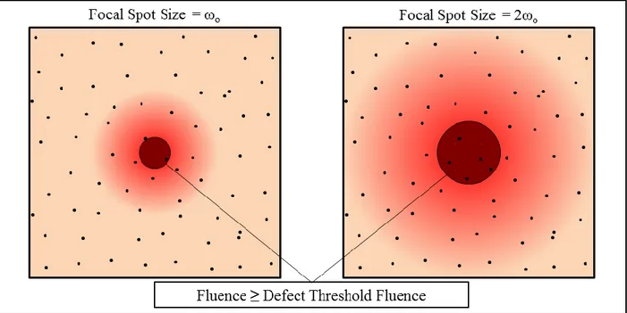
When keeping Fo constant, the theoretical damage probability directly depends on ωo2. Thus by using this model, which is graphically depicted in Fig. 1.2, one can realize that the measured damage probability at a given fluence level heavily relies on the focal spot size of the laser pulse exposure. This observation was readily observed during early investigations of laser damage [30]. Given this spot size dependence, the obvious response is to use larger spot sizes for testing. However, there is the added difficulty that during testing one must probe numerous fluence values to pinpoint Fth, there is a finite area to test given the size of the coated optic, and a spacing of at least 6ωo between test sites must be used to prevent cross-site contamination as prescribed by the ISO standard [20]. Furthermore, at the point where Fo is slightly larger than FD, the theoretical damage probability may be low enough such that an experimental value of 0% is still obtained over a finite number of test sites. The final conclusions to be drawn are that the ISO standard in the long-pulse regime results in substantial error and also overestimates Fth, which is very important when interpreting data and attempting to compare values for Fth from separate studies.
Figure 1.2: Schematic showing a random distribution of defects with a given fluence at which
they will initiate damage. The red regions depicts an incident gaussian pulse with a focal spot
size of ωo (left) and 2ωo (right). The shaded region indicates the region where the fluence is
greater than what is necessary for the defect to induce damage.
1.3 Laser Damage Thresholds: Current Status
Regardless of its limitations, using the ISO standard to quantify Fth has resulted in significant progress in advancing the fluence handling capabilities of optical coatings. Some of the most enlightening studies have been performed in the SPIE: Boulder Damage Symposium design competition, a double blind study intended to compare Fth of ICs from coating suppliers in industry and academia alike. In 2008, this competition investigated normal incidence high reflectors operating at λ=1064 nm and 5 nanosecond pulse duration [31], requiring a minimum reflectivity of 99.5% at the designed center wavelength. With thirty-five samples submitted, the range in Fth of the ICs was measured to span two orders of magnitude. The bulk of these samples utilized HfO2 or Ta2O5 as a high index material, and the deposition procecess varied between electron beam evaporation, ion assisted deposition, ion beam sputtering and magnetron sputtering. The highest Fth was measured for a coating deposited with electron
beam evaporation, exhibiting a value at nearly 130 J/cm2. The data demonstrate the prevalence of HfO2 as a high index material in obtaining a high damage threshold, where HfO2 designs had significantly higher Fth values than the HR designs using Ta2O5 as a high index material. In contrast, the results from the 2009 competition show that in the short pulse regime, Fth tends to vary far less among the twenty-five submitted samples [32]. Here HRs with greater than 95.5% reflectivity were irradiated with 200 fs pulses at a wavelength of 786 nm, with submitted samples deposited by the same various processes as in the 2008 competition. The maximum measured damage threshold was ~1.1 J/cm2, for a design utilizing HfO2 as the high index material.
To gain a better understanding of the current status of laser induced damage thresholdsin ICs, reported damage thresholds were compiled from twenty-four separate studies investigating laser damage at ~0.8 µm and ~1 µm, Fig. 1.3 [12, 31-53]. I have chosen to focus on more prolific HR and AR designs, but have also included several reports on single layers for reference. Notice that these studies are predominantly performed at a few nanosecond and sub- picosecond pulse durations, with very few studies in the several picoseconds to nanosecond range. This plot offers a very quantitative estimate as to the damage thresholds currently being obtained for IC structures operating at near-infrared wavelengths.
In the long pulse regime, AR and HR structures demonstrate similar performance, with Fth on the order of 10 – 130 J/cm2. This corresponds to peak intensities in the tens of gigawatts per square centimeter range. Given all of the data in this regime are at pulse durations around several nanoseconds, there is no clear trend in the pulse duration dependence of Fth. In the long pulse regime, work has shown a τ1/2
dependence of Fth for bulk materials, where τ is the laser pulse duration [15]. However, when investigating interference coatings the laser material interaction becomes far more complex. In the thin film materials used to fabricate interference coatings there are much larger defect concentrations than in bulk [54]. Furthermore, one needs to take into account interference effects that create variations in the
electric field distribution within the IC [55]. Interestingly, we see a similar trend to what was observed in the 2008 Boulder Damage Symposium design competition, where these reported damage thresholds vary by more than one order of magnitude.
10-14 10-13 10-12 10-11 10-10 10-9 10-8 10-7 1 10 100 m, AR m, HR m, single layer m, AR m, HR m, single layer
F
th(J cm
-2)
Pulse Duration (s)
Figure 1.3 Plot displaying Fth data from literature search of HR and AR ICs as well as single
layers. All materials are metal-oxides from various deposition processes [12, 31-53].
In the short pulse regime, Fth falls between several J/cm2 to a fraction of a J/cm2. One may also observe that the reported values for single layers tend to be quite higher than for the interference coatings. If data from single layers are omitted, a trend of increasing Fth values with increasing pulse duration is observed. Here the highest value of Fth is ~1.5 J/cm2 at a pulse duration of 350 femtoseconds. As the pulse duration is reduced below 100 femtoseconds, Fth tends to fall to a fraction of a J/cm2. Although these fluence values are much lower, the peak intensities in the short pulse regime are roughly two orders
of magnitude higher than in the long pulse regime, with values around several terawatts per square centimeter.
In the following sections I will divulge on experiments investigating laser induced damage of ICs. These results can be conceptually separated into two series of tests. In Chapter 2 I will discuss efforts directed toward laser induced damage in high reflection interference coatings when exposed to λ = 1.03 µm laser pulses. Modifications were made in material selection and the physical layered design. I will discuss how variation in designs impacts the optical properties of the ICs, as well as Fth in the long pulse regime. Chapter 3 investigates optical coatings for operation at 1.4 - 2 µm wavelengths in the short pulse regime; a parameter space previously unexplored by the laser damage community. In this work an optical parametric chirped pulse amplifier was fabricated and employed to carry out damage threshold measurements. The results for Fth are unprecedented, as the coatings damage at fluences near those of the fused silica substrates, showing deviation from what is expected in the literature and through modeling. Chapter 4 provides conclusions from these studies and covers future endeavors.
Chapter 2
Modification of Multilayer Mirror Top-Layer Design
for Increased Laser Damage Resistance
2.1 Background and Motivation
This chapter describes the results of experiments designed to optimize the performance of high reflectance interference coatings for high energy lasers producing near-infrared wavelength pulses in the nanosecond range. I specifically investigate the high reflector because of the prominent role it holds in the laser architecture. I show that the investigated design strategies significantly improve laser damage performance of the multilayer structures.
Ta2O5 is a prime candidate for a high index material in interference coatings given its low intrinsic stress [56], superior layer smoothness and uniformity [57], and low absorption and scattering losses. Ta2O5/SiO2 interference coatings are used for high average power lasers, such as the Laser Interferometer Gravitational Wave Observatory [58]. However, when paired with SiO2 to form a normal incidence high reflector at λ=1 m, designs employing HfO2 fair better than Ta2O5 in laser damage resistance when tested with pulses of a few nanoseconds in duration [31].
In a quarter wave reflector designed for = 1m, the electric field is maximum at the interfaces in which the high index material is deposited on the completed low index layer. The electric field decreases in amplitude and reaches the 1/e point within the first 5 or 6 quarter wave
pairs. Therefore, altering the top layers of the high reflector coating design is expected to modify the laser damage behavior. A previous theoretical development has been proposed for increasing the laser damage resistance of a multilayer high reflector by reducing the maximum electric field in the high index layers. This is realized through decreasing the thickness of the high index material and increasing the thickness of the low index material in the top few layers [58]. Experimental results following Apfel’s proposed design applied to TiO2/SiO2 multilayers demonstrated factors of increase in the λ = 1μm laser induced damage threshold fluence (Fth) as high as 2.6 at 30 ps pulse durations [60]. Another strategy proposed to increase the laser damage threshold focuses on reducing the electric field intensity at interfaces as opposed to in the high index material. It is proposed that gradient index profiles be utilized to shift the minima of the standing wave electric field distribution to the interfaces [61]. An ion beam sputtered HfO2/SiO2 refractive index step down design has also been investigated, where top high index layers are mixture layers with heavy concentrations of SiO2, gradually transitioning to pure HfO2 layers deeper into the stack. However, when irradiated with 12ns pulses from a Nd:YAG laser at λ=1μm, this design demonstrated a greater than 50% degradation in Fth compared with a typical HfO2/SiO2 quarter wave stack [62].
The motivation for this work is to investigate strategies to improve the laser damage resistance of Ta2O5/SiO2 coatings for applications in high energy lasers, while exploiting the benefits of the reduced stress and extremely low absorption losses not found in equivalent HfO2/SiO2 coatings. Our group has already demonstrated a 50 % increase in the laser damage threshold of a Ta2O5/SiO2 high reflection multilayer through replacement of Ta2O5 with HfO2 in the top three bilayers when tested using 350 ps pulses at λ = 1 μm [63]. In this work, the effect
of modifying the standing wave electric field distribution in the top few layers to increase the damage resistance of Ta2O5/SiO2 high reflectors is explored.
2.2 Experimental Procedure
2.2.1 High Reflector Design and Fabrication
Interference coatings based on Ta2O5/SiO2 were designed for normal incidence and 99.9% reflectivity at λ = 1μm. The coatings were deposited by ion beam sputtering (IBS) using a metal target for the reactive sputtering of Ta2O5 and a dielectric target for the deposition of SiO2. Further information on the deposition process has been presented elsewhere [63]. The interference coatings were deposited on one inch diameter, 0.25 in. thick fused silica substrates with a RMS roughness of 0.6 nm. No post annealing or ion assisting during growth was performed. Process conditions were optimized for each material, focusing on stoichiometric, amorphous growth with minimal intrinsic defect density. Our group has previously demonstrated the optimization of Sc2O3 thin films deposited with IBS, where process conditions were selected to minimize oxygen interstitial defects [16]. It is widely accepted that defects, both micron scale physical inclusions [64] and intrinsic intra-band state electronic defects [25], act as damage precursors in optical coatings for pulse durations ranging from several tens of picoseconds to the nanosecond regime.
The coating structure that was chosen as a reference is a quarter wave stack consisting of 15 pairs of Ta2O5/SiO2 layers, (Ta2O5/ SiO2)15. This design was modified to alter the standing wave electric field distribution in two ways. The first design involves adding an extra λ/4 layer of SiO2 to the top of the coating, which reduces the overall electric field due to enhanced constructive interference from reflections off the top air-coating interface and the successive
interfaces. For the second, reduced Ta2O5, design, the thickness of the top four Ta2O5 quarter wave layers was reduced to shift the peak of the electric field into the SiO2 layer as proposed by Apfel et al [59]. To the best of my knowledge, this technique has not yet been applied to the Ta2O5/SiO2 material system or for coatings for nanosecond to hundreds of picoseconds pulse duration applications. The electric field distribution in the quarter wave design and in the two modified coatings is plotted in Fig. 1 (a)-(c).
0.0 0.5 1.0 1.5 0 10 20 30 40 50 (a) Elec tric Fi eld (V/m ) 0.0 0.5 1.0 1.5 2.0 2.5 (c)
Figure 2.1 Standing wave electric field distribution in (a) the (Ta2O5/SiO2)15 base structure, (b)
the added λ/4 layer of SiO2, and (c) the reduced Ta2O5 thickness structure given an incident
intensity of 1 W/m2. The blue shaded regions represent the Ta2O5 layers.
2.2.2 Characterization and Laser Damage Testing
The normal incidence transmittance spectra from 190 to 1100 nm were measured for each structure with a Hitachi U-2010 spectrophotometer. Optical absorption in the structures was measured at λ = 1.06 μm with the photothermal common-path interferometry technique, yielding ppm resolution [65]. Further investigation of the surface of the structures was performed with atomic force microscopy for analysis of surface morphology and roughness.
Damage testing was performed using pulses from a Yb:YAG chirped pulse amplification laser system focused to a 1/e2 diameter of 90 μm [66-68]. Pulses of 300 fs duration from a
0.0 0.5 1.0 1.5
(b)
Yb:KYW oscillator are elongated to 190 ps in a grating stretcher. From here the pulses are sent through a 100 Hz rep rate Yb:YAG regenerative amplifier, yielding pulses with several millijoules of energy. Further amplification to tens of millijoules is performed in a cryogenically cooled “thick disk” Yb:YAG amplifier operating in an active mirror configuration. To generate the 4.4 ns pulses, the regenerative amplifier was operated as an unseeded Q-switched cavity, whereby subsequent amplification was performed in the same aforementioned amplifier.
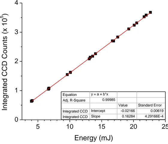
Damage testing was performed following ISO:21254 standards [20]. 100-on-1 testing was specifically carried out to more accurately portray a realistic Fth value of the mirror operating in a laser system when compared with 1-on-1 tests. The damage pulses were sent through a waveplate and polarizing beam splitter for energy tunability. Output from the helium neon laser was aligned collinear with the λ = 1.03µm damage beam using a beam combiner. Reflection from a fused silica wedge was used after the focusing lens and sent into the beam diagnostic CCD to evaluate the focal spot size and energy in-situ. From these CCD images, the pulse energy was obtained from integrating the counts on the CCD and referring to an energy calibration. The energy calibration was performed by simultaneously capturing images of the focused beam and measuring the energy that would irradiate the sample with a Newport 818-E energy meter. Figure 2.2 displays an experimentally obtained energy calibration, exhibiting excellent linear behavior.
Samples were held in a cell filled with nitrogen gas flowing at atmospheric pressure for the entirety of the testing. This flow was intended to remove any ablated material from redepositing on the test sample surface. A two-axis stage allowed for translation to a fresh site for each series of pulse exposures. Both this sample stage and the waveplate rotation were motor driven and controlled by a Labview ® program. Upon the users initiation, the program would
Figure 2.2 Experimental energy calibration with a linear least squares fit
site 1 mm away from the previous, following a square grid pattern. After irradiating ten sites, the waveplate motor rotates by a set increment to increase the energy. During exposures the user send a signal that simultaneously triggers the beam diagnostic CCD and opens a shutter for the 100 pulses to irradiate the sample. After exposure, the stage automatically translates to a fresh must continuously monitor the scatter CCD diagnostic to determine if the sample test site experienced damage.
From these measurements, the fluence is obtained for each exposure by calculating the beam energy and focal area from the CCD image. The peak fluence values are averaged for the series of ten exposures at the same waveplate setting. The 0% and 50% damage probability
5
10
15
20
25
0
1
2
3
4
In
te
g
ra
te
d
C
C
D
C
o
u
n
ts
(
x
1
0
5)
Energy (mJ)
Equation y = a + b*x Adj. R-Square 0.99985Value Standard Error Integrated CCD Intercept -0.02166 0.00619 Integrated CCD Slope 0.16284 4.29166E-4
Figure 2.3 Schematic of the optical setup for damage testing measurements. a) waveplate for
beam input, b) cube polarizer, c) Helium Neon laser, d) λ = .633 µm and λ = 1.03 µm beam combiner, e) 30 cm focusing lens, f) fused silica window, g) CCD for beam diagnostic, h) sample chamber, i) scatter detection CCD
probability curve does not always exhibit a clear linear trend, as displayed in Fig. 2.4. Krol et al have observed similar behavior in the damage probability curve for a single layer of Ta2O5 as is seen in Fig. 2.4b. In their case, the authors attributed the shape of the curve to a low density defect band that damages at low fluence combined with another defect type of higher density and higher damage fluence [69].
10 12 14 16 18 20 22 24 0 20 40 60 80 100 (a) Damage Probability (%) Fluence (J/cm^2) 5 10 15 20 25 0 20 40 60 80 (b) Damage Probability (%) Fluence (J/cm^2)
Figure 2.4 Damage probability curves for a) the base structure with 4.4 ns pulses and b) the +
λ/4 SiO2 structure with 0.19 ns pulses
2.3 Results
2.3.1 Surface and Optical Properties
Spectrophotometry was performed to ensure the transmittance curve matched the predicted curve from modeling in Essential Macleod software [4]. Table 2.1 displays the optical absorption losses at λ = 1.06 μm. The lowest optical absorption is observed in the structure with an added λ/4 layer of SiO2. This decrease in absorption is attributed to the lower overall electric field intensity in this coating structure. The largest optical absorption is observed in the reduced Ta2O5 structure. It has been previously demonstrated that post deposition annealing drives these optical absorption values lower [70].
The AFM micrographs in Fig. 2.5 show that the deposition a Ta2O5/SiO2 quarter wave stack actually results in a lower RMS roughness compared with the substrates. Furthermore, imperfections on the fused silica substrates from the polishing process are not observed after the deposition of the Ta2O5/SiO2 multilayers.
Table 2.1 Optical absorption loss measured at λ = 1 μm
2.3.2 Laser Damage Testing Results
Damage testing results are presented in Fig. 2.6, displaying the 50% damage probability (50%DP) and Fth for pulse durations of 4 and 0.19 ns. At both pulse durations, the added λ/4 top layer of SiO2 improves the 50% DP by over 100%. The structure with a modified electric field through shrinking the thickness of Ta2O5 layers demonstrates different behavior, showing a strong increase in the 50%DP in the ns regime, but demonstrating no advantage at 0.19 ns. No clear trend is observed in the damage onset for 0.19 ns pulse durations, however, at 4 ns an increase of ~80% is observed in Fth for both modified structures.
When comparing the values at each pulse duration, the ratio for Fth at 4 ns with respect to 0.19 ns ranges from 2-4 for the three structures. Following a √𝜏 dependence of the damage threshold where 𝜏 is the pulse duration, the expected ratio would be 4.81. These low Fth values at 4 ns compared with those at 0.19 ns may indicate a different initial damage mechanism leading to failure in the coating. Observing the damage curve in Fig. 2.4b, one may conclude that the low fluence tail may be due to defects that have been suppressed in some manner with the addition of the SiO2 capping layer, indicating a defect driven damage mechanism. However, the damage results at 4 ns do not demonstrate this same behavior. It has previously been demonstrated that SiO2 overcoats can increase the LIDT of a high reflector, where the effect was attributed to an
Sample Absorption Loss (ppm)
Ta2O5/SiO2 22.5
+ λ /4 SiO2 12.3
Figure 2.5 Atomic force microscopy micrographs of the surface of a) the fused silica substrate
and b) the Ta2O5/SiO2 quarter wave stack base coating structure. The scanned area is 5x5 μm
for each micrograph.
increase in the mechanical stability of the structure [71]. Therefore, fluences may be high enough such that delamination is occurring in the base structure irradiated with 4 ns pulses, and the added SiO2 in both modified designs improves the damage resistance of the coating due to an increased mechanical stability.
The damage morphologies in the (Ta2O5/SiO2)15 observed with a Nomarski microscope are displayed in Fig. 2.7. In these images, the layers can be observed by the rings about the center of the damaged region. In the case of the nanosecond damage morphology, the ablation of the coating has removed the entirety of the film to the substrate beneath. There is clearly evidence of thermal damage, where signatures of melting are observed at the periphery of the damage crater. The damage morphologies are similar at both pulse durations, however due to lower damage fluences in the 0.19 ns tests, the ablation region does not extend down to the substrate surface. Signatures of plasma scald are clearly seen outside the damage crater when the coatings are irradiated with the 4 ns pulses. These damage morphologies are similar in all the
Figure 2.6 Results from laser damage testing at 0.19 and 4 ns displaying 50% and 0% damage
probability fluence
Figure 2.7 Nomarski microscope images of the damage morphology at 0.19 and 4 ns for the
quarter wave structure (Ta2O5/SiO2)15.
0 10 20 30 40
.19 ns
4 ns
+ /4 SiO2 + /4 SiO2 Reduced Ta2O 5 Reduced Ta2O 5 Ta2O5 /SiO2 Ta2O5 /SiO2Fl
u
en
ce
(J/
cm
^2
)
0 % Damage Prob 50% Damage Prob2.4 Conclusions
(Ta2O5/SiO2)15 high reflector interference coatings for λ = 1 μm were fabricated using ion beam sputtering. Modifications to the design of the quarter wave stack base coating structure include reduced thickness of the top four Ta2O5 layers in favor of SiO2 and addition of a λ/4 SiO2 capping layer. Surface smoothing to a roughness below that of the substrate and low absorption losses at λ = 1.06 µm are reported for the structures without a post anneal treatment. Laser induced damage threshold measurements were performed, demonstrating increases in the 50%DP by over 100% at both 0.19 and 4 ns pulse durations when adding an extra λ/4 SiO2 layer. Reducing the thickness of Ta2O5 in the top of the structure to reduce the electric field in these layers produces inconclusive results, where an improvement in the 50%DP is observed at 4.4 ns and no effect is observed at 0.19 ns. No conclusive increases in the onset fluence are observed at 0.19 ns, while ~80% increases are observed with 4 ns pulses. The data do not correlate with a √𝜏 fit, which suggests different damage mechanisms at the two pulse durations.
This research was performed in collaboration with Dr. Wolfgang Rudolph’s group at the University of New Mexico. The work was presented at the 2014 Boulder Damage Symposium and published in the corresponding proceedings [72]. Results from this Chapter were also presented at 2014 CLEO conference for laser science [73].
Chapter 3
ULTRA HIGH DAMAGE THRESHOLD INTERFERENCE COATINGS FOR
NEXT GENERATION ULTRAFAST INFRARED SOURCES
3.1 Background and Motivation
The large number of applications requiring ultra-high intensity pulses at wavelengths longer than output from traditional chirped pulse amplification (CPA) lasers, i.e. 0.8 µm, have motivated the rapid development of sources based on optical parametric chirped pulse amplification (OPCPA). Additionally, since wavelengths in this region are strongly absorbed in the cornea and lens, reducing the chance of damage to the retina, there are a large number of remote-sensing applications which employ "eye-safe" solid state lasers at wavelengths longer than 1.3 μm. However, although multilayer dielectric interference coatings play a crucial role in development and scaling of these cutting edge sources, there have been no studies of short-pulse damage thresholds of interference coatings in this wavelength region. I demonstrate interference coatings for 1.6 µm wavelength based on stacks of metal oxides that do not damage at fluences of up to ~7.0 J/cm2 and 3.5 TW/cm2 peak intensities when tested with picosecond duration pulses. These fluence values are near Fth of the infrared grade fused silica substrates the ICs are deposited on. This behavior challenges current understanding of short pulsed laser damage as the damage threshold fluence appears largely unimpaired by the dominance of nonlinear absorption processes and by electric field interference effects.
The development of optical parametric chirped pulse amplifiers (OPCPA) has made ultra-high intensities at near to mid-infrared (IR) wavelengths beyond one micron accessible. Ultra-short pulse mid-IR sources have been utilized in high harmonic generation schemes to extend the cut-off frequency [74-76], and as drivers for incoherent hard x-ray sources [77]. OPCPAs pumped with one micron wavelength, several picosecond pulse duration driver lasers have been established as a third generation of femtosecond laser technology that is still in developmental stages. Such sources promise unprecedented peak intensities at kilowatt average powers [78]. Interference coatings (ICs) are essential to the laser architecture, where antireflection (AR) coatings layer the faces of crystal gain media and high reflectors (HR) direct the beam with minimal losses. Specifically in an OPCPA system, ICs are subject to stringent design concerns, where extensive variability in the wavelength and pulse duration needs to be considered. With continual progress toward record high peak intensities, a detailed understanding of damage initiation mechanisms in ICs is essential to the success of these research efforts.
There are numerous studies on the behavior of dielectric oxides when exposed to picosecond and femtosecond pulses at specific wavelengths common to conventional short pulse laser sources, i.e. ~0.8 µm and 1 m corresponding to the output from the Ti:sapphire and doped YAG lasers, respectively [79-82]. At these near infrared (NIR) wavelengths and pulse durations below a few picoseconds, laser damage in dielectric oxides is ascribed to electronic instabilities that arise when a critical electron density is reached via predominantly multiphoton, tunneling, and impact ionization [21]. The multiphoton and tunneling ionization rates in a monochromatic field were derived by Keldysh, demonstrating an inverse proportionality with the band gap of the material [83]. The importance of these ionization processes has been confirmed
experimentally by studies that show the threshold laser fluence required for damage (Fth) in oxides scales with the bandgap of the dielectric and the pulse duration [83]. The wavelength dependence of multiphoton ionization was theoretically investigated and experimentally confirmed in TiO2 [85]. Here an increase in Fth was observed by transitioning from a two to three photon absorption regime when the incident pulse wavelength exceeded ~680 nm. Based on these findings, high band gap materials are utilized, where oxide ICs for short-pulse exposure are typically designed as stacks of high index layers of HfO2 and low index layers of SiO2.
Using these design considerations I have engineered dielectric metal oxide ICs with center wavelength of 1.6 m. I present measurements of the damage threshold of interference coatings operating in the short pulse regime at a wavelength longer than 1.06 um for the first time. I show that these ICs are characterized by at wavelength Fth values of nearly 7 J/cm2 when irradiated with pulses of 2 picosecond duration, a value approaching Fth of the infrared fused silica substrates, which are specifically manufactured with an -OH content less than 1000 ppm. These encouraging results demonstrate that with appropriate selection of materials and coating structure it is possible to realize ICs with unprecedented laser damage performance not observed at =1 µm, challenging the established understanding of short pulse laser damage in dielectric oxides.
3.2 Experimental Procedure
3.2.1 Interference Coating Design and Fabrication
Thin film ICs were deposited by ion beam sputtering on 1 in. diameter, 0.25 in. thick high quality infrared grade fused silica substrates using conditions previously reported [63], where optimization of the oxygen partial pressure during growth leads to minimal absorption loss [16].
Different coating materials were used in the design of 1.6 μm wavelength HRs with greater than 90% reflectivity, [H/L]6, where “L” indicates a quarter wave of low index SiO2 and “H” was selected as a quarter wave of Ta2O5, Y2O3, or HfO2. A six layer HfO2/SiO2 AR coating was fabricated for operation at a center wavelength of λ = 1.6 μm. Coating thicknesses ranged from 1.70 μm for the AR to a maximum thickness of 2.94 μm for the Y2O3 HR structure.
The standing wave electric field distribution within the IC structures was calculated with Essential Macleod software [4], and is presented in Fig. 3.1a and Fig. 3.1b for the HfO2/SiO2 HR and AR structures, respectively. These plots demonstrate that during exposure to an incident pulse, the peak electric field in the uppermost HfO2 layer is nearly 70% higher than what is observed in the AR design. However, the electric field intensity in the HfO2 layer at the substrate interface is nearly three times lower in the HR design compared with the AR design. This is evidenced by the photothermal common-path interferometer absorption scans in Fig. 3.1c and Fig. 3.1d, where absorption in the substrate is clearly seen in the AR structure, but not in the HR structure due to the low transmission of the coating. Using this technique, it is feasible to resolve sub-ppm absorption in the ICs, where the peak interference signal is directly proportional to the absorption in the IC [65]. The absorption loss of each structure measured at λ=1.55 μm is displayed in Table 3.1. Using Ta2O5 and HfO2 high index materials in the HR designs results in ultralow sub-6 ppm absorption loss levels. The Y2O3/SiO2 HR and the HfO2/SiO2 AR have absorption losses of 17 and 22 ppm respectively. These low absorption losses are obtained without any post-process annealing, indicating the excellent quality of the coatings.
0.00 0.25 0.50 0.75 1.00 1.25 1.50 0 10 20 30 40 50 60 a) HfO 2 HR (top 6 layers) El ectric F iel d Inten sity (V/m)
Optical Thickness from Air
0.00 0.25 0.50 0.75 1.00 1.25 1.50 1.75 0 10 20 30 40 50 60 b) HfO 2 AR El ectric F iel d Inten sity (V/m)
Optical Thickness from Air
0 1 2 3 4 5 6 7 8 0.0 0.2 0.4 0.6 0.8 1.0 c) Film Absorption Air HfO2 HR Normal iz ed Ab sorptio n Si gnal Position (mm) 0 1 2 3 4 5 6 7 8 0.0 0.2 0.4 0.6 0.8 1.0 d) Film Absorption Air Substrate Absorption Normal iz ed Ab sorptio n Si gnal Position (mm) HfO2 AR
Figure 3.1 Standing wave electric field distribution in the a) HfO2/SiO2 HR and b) HfO2/SiO2
AR structures for an incident intensity of 1 W/m2. Red shaded regions indicate HfO2 and grey
shaded regions represent SiO2. Normalized photothermal common-path interferometer z-scans of
the c) HfO2/SiO2 HR and d) HfO2/SiO2 AR structures.
Table 3.1 Optical absorption of interference coating structures at λ = 1.55 μm
Sample Absorption Loss (ppm)
Ta2O5 HR 5.6 ± 0.3
HfO2 HR 5.9 ± 0.3
Y2O3 HR 17.1 ± 0.9
3.2.2 Optical Parametric Chirped Pulse Amplifier Design
The laser damage performance of the 1.6 m ICs was tested at-wavelength using the 2 ps pulse duration output from an OPCPA system. Pulses with a 1.5-2.0 µm variable wavelength were generated utilizing a series of non-collinear optical parametric, chirped pulse amplifying stages. The “frontend” of this system, illustrated in Fig. 3.2a, is dedicated to generating the NIR seed pulses using a technique similar to that previously reported by Homan et al. [86]. Pulses from a diode-pumped, mode-locked Yb-KYW oscillator are amplified by a Yb:KYW regenerative amplifier and compressed, resulting in ~100 µJ, 600 fs duration pulses. 10% of the pulse energy is split off and focused into a 1 cm thick undoped YAG crystal, generating a white light continuum to act as the seed for NIR generation. The remaining pulse energy is frequency doubled by a BBO crystal generating λ = 0.515 m wavelength pulses with a conversion efficiency of ~25%. The 0.515 m pulses are separated from the remaining 1.03 m and are focused along with the white light seed into a 6 mm thick BBO crystal to produce NIR idler pulses via type-I difference frequency generation (DFG). Due to phase-matching conditions, tuning of the non-collinear and phase-matching angle allows for wavelength tuning of the DFG output in a range of 1.5-2.0 µm. These NIR pulses seed a type-II optical parametric preamplifier in a 6 mm thick KTP crystal, where pump pulses are taken from the undoubled λ = 1.03 µm radiation in the aforementioned frequency doubling process. The resulting non-colinearity angle is adjusted to maximize amplification of the NIR pulses. The end result is NIR wavelength tunable pulses with several microjoules of energy. Figure 2b displays three wavelength spectra measured with a scanning grating monochromator, demonstrating the tunability of the source.
The “backend” of the system is comprised of three optical parametric amplifiers, Fig 3.3a. These are pumped by an all-diode-pumped cryogenically cooled CPA Yb:YAG laser that
Fig. 3.2 a) Schematic of the OPCPA frontend setup and b) three wavelength spectra
demonstrating source tunability.
is seeded by the same Yb:KYW mode-locked oscillator, providing passive temporal synchronization of the pump and seed pulses in the OPCPA stages. For this setup, the two amplification stage laser system produced 50 mJ, λ = 1.03 µm pulses with 5 ps FWHM duration at 100 Hz repetition rate. Further details on the pump laser are presented elsewhere [66-68]. The pulses from the IR seed generation are grating stretched to durations of ~2 ps FWHM, which is well within the 5 ps pump pulse duration. The pump pulses are split into three beamlines with a pair of thin-film beam splitters, such that pump energy increases by roughly one order of magnitude for each successive stage of OPA. Type II KTP is utilized for each OPA stage with crystal thicknesses ranging from 6 mm for the first two stages to 10 mm for the final stage. After final amplification, ~5 mJ pulses (Fig. 3b) in a wavelength tunable range of 1.5-2 μm and uncompressed pulse durations of 2 ps FWHM are obtained. For the results presented here, these amplified pulses were not recompressed.
Figure 3.3 a) Schematic of the OPCPA backend and b) OPCPA energy output as a function of
3.2.3 Laser Damage Measurements
For laser damage testing the OPCPA source was angle-tuned to emit a center wavelength of 1.6 μm. A 100-on-1 damage testing protocol was implemented to quantify Fth. This type of testing provides a more realistic assessment of the fluence at which the coatings will damage during extended operation. The NIR pulses were focused to a 1/e2 diameter of 80 µm. The pulse energy was selected with a waveplate and polarizing beam splitter and measured with a Newport 818-E energy meter. The focused beam profile was measured using the knife edge technique. Ten separate test sites were illuminated at a selected fluence to determine the damage probability. Damage events were identified as any permanent increase in scatter from an incident Helium Neon laser imaged onto a CCD detector. Confirmation of damage sites was performed by post-test analysis with a Nomarski microscope and a 100x objective. The Fth values displayed in Fig. 3.4 are reported as the average of the highest measured fluence with no observed damage events and the next fluence level where a non-zero damage probability was obtained.
The results of Fig. 3.4 show HfO2/SiO2 and Y2O3/SiO2 HRs achieve an Fth ~7.0 J/cm2 that is very near that of the infrared fused silica substrate, 7.5 J/cm2. At this fluence the coating structures are irradiated at peak intensities of 3.5 TW/cm2. Fth for the Ta2O5/SiO2 HR is 4.1 J/cm2, a 40% reduction from the HfO2/SiO2 structure. However, this Ta2O5/SiO2 HR exhibits a Fth over four times higher than what has been measured for a comparable Ta2O5/SiO2 HR using 1.8 ps duration pulses at λ = 0.8 m [87]. Fth for the HfO2/SiO2 AR coating is 6.3 J/cm2. There is no correlation between the measured optical absorption in Table 1 and Fth of the IC structures. In fact, the Ta2O5/SiO2 HR, which demonstrates the lowest absorption loss, damages at a lower fluence. These linear absorption measurements probe the intrinsic defects within the
amorphous structure of the coatings [16]; therefore I conclude that damage initiation is not reliant on this class of defects.
0 2 4 6 8 Th res ho ld Fl uence (J/ cm 2 ) Y2O3 HR
Ta2O5 HR HfO2 HR HfO2 AR IR Fused Silica
Figure 3.4 Measured damage threshold fluence for interference coatings at λ = 1.6 m. Error bars are taken from the measured standard deviation in both the pulse energy and beam area.
3.2.4 Damage Morphologies
Post inspection of the damage sites was performed with a Zygo, NewView 7300 coherence scanning interferometer. The instrument was set up with a 50x objective yielding a 0.44 μm lateral resolution and sub-nm resolution in the scanning axis. Figure 3.5, displays three dimensional micrographs and crater depth of the damage sites at a fluence that resulted in a measured damage probability nearest to fifty percent. Damage in fused silica is evidenced by craters ~40 micron in depth. Similarly, for designs employing HfO2 and Y2O3 as a high index material, laser damage propagates into the substrate. At the lower Fth experienced by the Ta2O5/SiO2 HR structure, a flat bottom crater morphology is observed where the coating is
mainly ablated. There was no evidence of nodular ejection pits in the coating, as these types of defects are typically absent in IBS coatings. The bottom row of Fig. 3.5 displays Nomarski microscope images of the damage craters. Evidence of spallation is observed by debris deposits around the damage crater. Fused silica demonstrates thermal-stress induced fractures at the periphery of the damage crater. Others have shown that under λ=800 nm irradiation with sub-ps pulses, ion beam sputtered HfO2 coating damage morphologies vary between clean ablated regions and ablation with signs of melting, suggesting thermal mechanisms may also be involved [88]. Delamination of SiO2 top layers in Ta2O5/SiO2 quarter-wave reflectors has also been observed, attributed to preferential ablation of the lower band gap Ta2O5 material beneath the SiO2 top layer [89].
Figure 3.5 (Top) Coherence scanning interferometer micrographs of damage morphology at
fluence levels yielding a damage probability nearest to 50%. Incident fluence and crater depth are displayed. Scan size is 0.28 x 0.21 μm. (Bottom) Nomarski microscope images of damage morphologies. Image size is 150 x 150 μm.
3.3 Rate Equation Modeling
Ionizing laser damage may be modeled by a rate equation tracking the time dependent conduction electron density (ne) in the wide band gap dielectric material [15, 21].
𝐝𝐧𝐞
𝐝𝐭 = 𝐖𝐩𝐢+ 𝐖𝐚𝐯𝐧𝐞(𝐭) (3.1)
Here Wpi is the combined rate of multiphoton and tunnel ionization and Wav is the rate of avalanche ionization, the process where a conduction band electron has gained sufficient kinetic energy via photo-absorption to promote a valence electron in a collisional process. The damage criterion sets Fth as the fluence necessary to create a conduction band electron density equal to the critical plasma density in the material, whereby the remaining laser pulse is strongly absorbed.
I invoke such a formalism using numerical methods to evaluate Fth. The combined multiphoton and tunneling ionization rate is taken from the derivation by Keldysh [83]. Wpi strongly depends on the intensity within the laser pulse and accounts for the order of multiphoton absorption, defined as the number of photons required to traverse the band gap of the material. The rate of impact ionization (Wav), taken from Vaidyanathan et al, simultaneously accounts for electron heating by inverse bremsstrahlung as well as electron-phonon relaxation processes [90]. It is noted that when using such a model, Fth varies significantly with the electron collision rate, 1/τk. Using a value of 2x10¹⁵
s for τk, I have obtained results for the pulse duration dependence of Fth in fused silica at λ = 1053 nm that agree well with experimental data from Stuart et al. [15].
Table 3.2 displays the calculated damage threshold fluence resulting from this model applied to different metal-oxide single layers at 1.0 and 1.6 µm wavelengths, considering an incident Gaussian pulse of two picosecond duration. The Keldysh parameter at the peak
intensity varies from ~3-4 for these calculations, indicating that multiphoton absorption is the more prominent ionization mechanisim compared with tunneling. The first trend one notices is this model predicts a lower threshold fluence at λ = 1.6µm. This trend is attributed to the increase in the avalanche ionization rate and reduction in the plasma frequency with increasing wavelength, however, the wavelength dependence of electronic damage has been shown to be rather complex [14]. One also sees a strong reduction in Fth with lower band gap materials; as high as 55% comparing SiO2 to Ta2O5. This effect is a direct consequence of the increase in multiphoton and tunnel ionization rates with lower band gap materials, as was discussed previously [83].
Table 3.2 Calculated Fth values of several metal-oxide single layers from the rate equation
model for 2 ps pulse durations and wavelengths of 1.0 µm and 1.6 µm. Also displayed is the
material band gap and refractive index used for the calculation. HfO2 and Y2O3 are displayed in
one row given the similar band gap and refractive index values for these materials
Material Band Gap
(eV) Refractive Index Fth (Jcm-2) λ = 1.0 µm Fth (Jcm-2) λ = 1.6 µm SiO2 8.3 1.45 2.36 1.52 HfO2 & Y2O3 5.1 2.0 1.53 0.99 Ta2O5 3.8 2.1 1.14 0.68
When applying such a model to our experimental data several discrepancies arise. The model predicts a band gap dependence for Fth that is not observed experimentally in HfO2/SiO2 and Y2O3/SiO2 ICs. These ICs utilize high index materials of lower band gap compared to SiO2
that should increase the ionization rates, leading to an overall reduction in Fth as is evident in the model. However, comparing the Ta2O5/SiO2 HR with the HfO2/SiO2, the band gap trend predicted by the model is observed.
Interference effects are also not evident in the laser damage behavior of the ICs investigated. Interference effects in the HR design lead to significant increases in the standing wave electric field that should reduce Fth in relation to the value of the AR coating and the substrate. Chen et al. have shown that by modifying the HR design to reduce the peak electric field in the high index layers of a HfO2/SiO2 high reflector, increases in Fth of 15-20% may be obtained at pulse durations below 150 fs [36]. Furthermore, Yuan et al. used similar modeling to predict the lower measured Fth of a HfO2/SiO2 HR coating compared with a HfO2 single layer at λ = 0.8 m [91]. However, it seems one cannot utilize a similar approach here as Fth for the HfO2/SiO2 HR and AR structures is similar, in spite that the peak electric field in the HfO2 layers of the HR design is 70% higher than in the AR design, Fig 3.1.
3.4 Conclusions
In this chapter, I have demonstrated ultra-low loss ion beam sputtered HR and AR coatings for operation at 1.6 µm wavelengths. I show for the first time, these coatings damage at fluences approaching 7.0 J/cm2, nearing the threshold of the fused silica substrates when tested at 2 ps pulse duration. These experimental results challenge the current understanding of laser damage, where interference effects and lower band gap materials do not consistently impair Fth. This unprecedented performance is unlike that observed in the 0.8-1 m wavelength range at similar pulse durations, where the coatings damage at significantly lower fluences compared to the substrate. These ultra-high damage threshold ICs enable laser architectures that are not exclusively limited in energy output by the damage thresholds of the ICs. There are also
significant advantages in knowing that Fth is relatively consistent across the varying optical elements required to fabricate an OPCPA system.
Chapter 4
Conclusions and Future Work
The scope of this thesis has covered laser damage studies of ion beam sputter deposited interference coatings for pulse durations from several nanoseconds to a few picoseconds, and wavelengths from 1 – 1.6 µm. To realize these experiments, two radically different sources were utilized, a Yb:YAG chirped pulse amplification system and an optical parametric chirped pulse amplification system.
The first experimental studies in Chapter 2 explored design modifications to ion beam sputter deposited Ta2O5/SiO2 high reflectors to increase Fth. Laser damage testing was performed at 0.19 and 4 ns pulse durations at 1.03 µm wavelength. These studies illustrate the importance of added silica in the HR design, where increases in the 50% damage probability of over 100% were observed at both pulse durations. The structure with an added SiO2 capping layer demonstrated the highest measured damage threshold of 25 J/cm2 at a pulse duration of 4 ns. Although HfO2/SiO2 designs tend to outperform Ta2O5/SiO2 in terms of laser damage performance, Ta2O5 has numerous other attractive properties that necessitate its use in ICs for high energy lasers. Ta2O5 based ICs demonstrate incredibly smooth surfaces, exhibit low stress when deposited by ion beam sputtering, and offer higher reflection bandwidth due to a higher refractive index. Furthermore, the presented design strategies should be applicable to other material systems.
This thesis also presents the first comprehensive study of damage thresholds of ICs at 1.6 µm wavelength and two picosecond pulse durations. AR and HR ICs were demonstrated with
ultralow absorption losses at 1.6 µm wavelengths. For the damage testing, an OPCPA source was developed, generating 5 mJ pulses with a tunable wavelength between 1.5-2 µm. These ICs exhibit Fth values approaching Fth of the infrared grade fused silica substrates. Employing a common rate equation model, the obtained Fth values were shown to deviate from the expected behavior, where interference effects did not seem to degrade the laser damage resistance, and only Ta2O5 demonstrated the expected reduction in Fth due to a much smaller band gap than SiO2. Similar modeling has proved fully adequate at describing Fth results for single layers at 0.5 µm λ ≤ 1 µm.
Future work on high reflectors will be heavily devoted toward refining modified designs and extending these strategies to various other types of ICs, especially ARs. Further design considerations will include studies elucidating the effects of interfaces on the laser damage performance. On the experimental end, adding a grating compressor to the Yb:YAG laser system will then allow for damage threshold testing at three separate pulse durations from several picoseconds to a few nanoseconds. These studies may provide insight into how the modified designs behave in short pulse damage regime.
Results from Chapter 3 will be extended to 2 µm, covering the full tunability of the current OPCPA architecture to explore the wavelength dependence of laser damage in this short pulse regime. This research will then continue deeper into the IR, investigating longer wavelengths at 4 – 6 µm to test the efficacy of ICs and their laser damage behavior in the mid-infrared regime. Due to the necessary increase in layer thicknesses at these wavelengths, a new methodology may be required in the deposition of the ICs to ensure low losses and high surface quality. This will also require modifications to the OPCPA for generating mid-infrared pulses with sufficient energy to assess Fth in the ICs.
REFERENCES
1) P. W. Baumeister, "Optical interference coatings," Appl. Opt 15, 2313 (1976). 2) P. Baumeister, Optical coating technology (SPIE Press Bellingham, 2004). 3) N. Kaiser, and H. K. Pulker, "Optical interference coatings," (Springer, 2003). 4) A. Macleod, "The Essential Macleod," software by Thin Film Center Inc (1997). 5) A. Tikhonravov, and M. Trubetskov, "OptiLayer thin film software," (2003).
6) D. L. Windt, "IMD—Software for modeling the optical properties of multilayer films," Computers in physics 12, 360-370 (1998).
7) J. B. Alameda, T. W. Barbee, W. M. Clift, J. A. Folta, B. Kaufmann, and E. A. Spiller, "Improved reflectance and stability of Mo-Si multilayers," Optical engineering 41, 1797-1804 (2002).
8) A. Ghosh, P. Kant, P. Bandyopadhyay, P. Chandra, and O. Nijhawan, "Antireflection coating on germanium for dual channel (3–5 and 7.5–10.6 μm) thermal imagers," Infrared physics & technology 40, 49-53 (1999).
9) K. Yang, X. Long, Y. Huang, and S. Wu, "Design and fabrication of ultra-high precision thin-film polarizing beam splitter," Optics Communications 284, 4650-4653 (2011).
10) V. Pervak, C. Teisset, A. Sugita, S. Naumov, F. Krausz, and A. Apolonski, "High-dispersive mirrors for femtosecond lasers," Optics express 16, 10220-10233 (2008).
11) M. L. Grilli, F. Menchini, A. Piegari, D. Alderighi, G. Toci, and M. Vannini, "Al 2 O 3/SiO 2 and HfO 2/SiO 2 dichroic mirrors for UV solid-state lasers," Thin Solid Films 517, 1731-1735 (2009).
12) M. Jupé, M. Lappschies, L. Jensen, K. Starke, and D. Ristau, "Laser-induced damage in gradual index layers and Rugate filters," in Boulder Damage Symposium XXXVIII: Annual Symposium on Optical Materials for High Power Lasers(International Society for Optics and Photonics), pp. 640311-640311-640313 (2006).
13) L. Gallais, H. Krol, J.-Y. Natoli, M. Commandre, M. Cathelinaud, L. Roussel, M. Lequime, and C. Amra, "Laser damage resistance of silica thin films deposited by electron beam deposition, ion assisted deposition, reactive low voltage ion plating and dual ion beam sputtering," Thin Solid Films 515, 3830-3836 (2007).
14) M. Jupé, L. Jensen, K. Starke, D. Ristau, A. Melninkaitis, and V. Sirutkaitis, "Analysis in wavelength dependence of electronic damage," in Laser Damage Symposium XLI: Annual Symposium on Optical Materials for High Power Lasers(International Society for Optics and Photonics), pp. 75040N-75040N-75012 (2009).
15) B. C. Stuart, M. D. Feit, S. Herman, A. M. Rubenchik, B. W. Shore, and M. D. Perry, "Nanosecond-to-femtosecond laser-induced breakdown in dielectrics," Physical Review B 53, 1749-1761 (1996).