DEGREE PROJECT, IN ELECTRONICS AND COMPUTER ENGINEERING , FIRST LEVEL
STOCKHOLM, SWEDEN 2015
Automatic Probing System for PCB
ANALYSIS OF AN AUTOMATIC PROBING
SYSTEM FOR DESIGN VERIFICATION OF
PRINTED CIRCUIT BOARDS
ALVE AALTO AND ALI JAFARI
Kungliga Tekniska Högskolan
Examinator: Anders Västberg, vastberg@kth.se
Handledare: Jens Axelsson, Ericsson, jens.j.axelsson@ericsson.com Författarens e-postadress: alvea@kth.se, alijr@kth.se
Utbildningsprogram: TIEDB, 180hp Omfattning: 9528 ord exklusive bilagor Datum: 2014-10-08
Examensarbete/projektrapport inom
Elektronik och Datorteknik 15 poäng
Automatic probing system for
PCB
Analysis of an automatic probing system for design
verification of printed circuit boards.
Abstract
The purpose of this thesis is to conduct an analysis of whether the printed circuit boards from Ericsson can be tested using an automatic probing system or what changes in the design are required, to be a viable solution. The main instrument used for analyzing the printed circuit board was an oscilloscope. The oscilloscope was used to get the raw data for plotting the difference between the theoretical and actual signals. Connected to the oscilloscope was a 600A-AT probe from LeCroy. The programs used for interpreting the raw data extracted from the oscilloscope included Python, Matlab and Excel. For simulations on how an extra via in the signal path would affect the end results we used HFSS and ADS. The results were extracted into different Excel sheets to get an easier overview of the results.
The results showed that the design of a board must almost become completely rebuilt for the changes, and it is therefore better to imple-ment in a new circuit board rather than in an already existing one. Some of the components have to either be smaller or placed on one side of the board, where they cannot be in the way of the probe. The size of the board will become larger since the rules of via placements will be limited compared to before. The most time demanding part was the simulations of the extra via in the signal path, and the results showed that if a single-ended signal is below two gigahertz the placing of the via does not make a big difference, but if the signal has a higher frequency the placement is mostly dependent on the type of the signal. The opti-mal placement is generally around four millimeters away from the receiving end.
Keywords: Flying probe tester, PCB design, Python programming, Matlab programming, robotic probes, Em problems, PCB test, ADS, HFSS.
Sammanfattning
Målet med detta examensarbete är att göra en analys av huruvida Ericssons kretskort kan testas med hjälp av ett automatiskt probe system eller om det kräver stora förändringar i designdelen av kretskorten och om, vad för förändringar det i sådant fall kan vara. Till hjälp att analy-sera kretskorten har vi haft oscilloskop för att få ut rådata om skillna-derna mellan de teoretiska och verkliga signalerna. För att kunna tyda oscilloskopets samplade signaler har olika programmeringsspråk som Python, Matlab samt Excel använts. En extra via i signalens väg har även simulerats i HFSS och ADS med olika sorts probar för att se hur signalens beteende påverkas. Resultaten extraherades sedan in i olika Excel ark för att få en lätt överskådlig bild av resultaten.
Resultatet vi fick visade att utformningen av ett kretskort med ändring-arna skulle vara lättare att göra med en ny design istället för en redan existerande då större delar av kortet skulle behöva göras om. Vissa stora komponenter behöver antingen göras om, hitta mindre men likvärdiga eller sättas på ena sidan av kortet där de inte är i vägen för proben. Kretskorten som kommer använda flygande probesystem kommer antagligen bli lite större då viornas placering är mer begränsade än tidigare. Det mest tidskrävande arbetet var att simulera olika placering-ar av en extra via i signalens väg. Detta visade att på en single ended signal under två gigahertz så gör det ingen större skillnad vart i signa-lens väg som den extra vian placeras. Då en högre frekvens används så är själva signalens karaktär det viktigaste än placeringen av en via, men om man inte vet den exakta karaktären så är fyra millimeter bort från mottagarens sida att rekommendera då närmare placering av viorna gör att signalerna börjar störa varandra.
Nyckelord: Flying probe tester, PCB-design, Python programmering, Matlab programmering, automatiska probar, EM problem, PCB-test, ADS, HFSS.
Acknowledgements
A sincere thank you to all the people at the Ericsson Radio and PCB divisions for lending us their time and expertise.
Table of Contents
Abstract ... II Sammanfattning ... III Acknowledgements ... IV Terminology ... VII
Abbreviations and acronyms ... VII List of figures ... IX
1 Introduction ... 1
1.1 Background and problem motivation ... 1
1.2 PCB background ... 1
1.3 Probe background ... 1
1.3.1 Flying probe background 2 1.4 Limitations ... 2 1.5 Problem definition ... 3 2 Theory ... 4 2.1 PCB Materials ... 4 2.2 Transmission line ... 5 2.2.1 Impedance 5 2.2.2 Stripline 7 2.2.3 Angle (Bend) 9 2.2.4 Length matched 10 2.2.5 Single-ended 10 2.2.6 Differential 11 2.3 Via... 11 2.3.1 Blind via 12 2.3.2 Buried via 12 2.3.3 Through hole via 12 2.3.4 Stub 12 3 Methodology ... 14
3.1 Printed Circuit Board check... 14
3.2 Oscilloscope measurements ... 15
4 Results ... 23 4.1 Simulation Results ... 23 4.2 PCB Measurement Results ... 27 5 Discussion ... 30 5.1 Simulations/Hardware ... 30 5.2 Conclusions ... 31 5.3 Future Work ... 32 Reference List... 33
Terminology
Abbreviations and acronyms
ADC Analogue to Digital Converter
ADS Advanced Design System
ASIC Application Specific Integrated Circuit
CML Current Mode Logic
CPU Central Processing Unit
DAC Digital to Analogue Converter
DC/DC DC-DC converter
DFT Design for Testing
FG Function Generator
FPGA Field Programmable Gate Array
HFSS High Frequency structural simulator
IC Integrated Circuit
I2C (also IIC) Inter IC Control
I/O Input/Output
LTU Local Timing Unit
LVDS Low Voltage Differential Signaling
MUX Multiplexer
RU Radio Unit
RX Receiver
SIS Signal Integrity Simulation
SPI Serial Peripheral Interface
SW Software
TRX Transceiver
TX Transmitter
List of figures
Fig. 1: The buildup of a symmetric PCB, made out of copper and FR4.
Fig. 2: How the currency moves in two transmission lines.
Fig. 3: A microstrip line in cross section.
Fig. 4: A differential microstrip line in cross section.
Fig. 5: A symmetric stripline in cross section.
Fig. 6: A differential symmetric stripline in cross section.
Fig. 7: Shows a “mitered” bend.
Fig. 8A: Shows the output of a length matched differential pair.
Fig. 8B: Shows the output of a non-length matched differential pair.
Fig. 9: Shows the three most common types of via; blind, buried and
through vias.
Fig. 10: Shows a thermal via.
Fig. 11: A through via where the transmission line changes layer.
Fig. 12: Where a flying probe cannot reach to probe.
Fig. 13: A pair of vias put at a specific distance from the other vias to
measure the impact of an extra via.
Fig. 14: The buildup of our design in HFSS.
Fig. 15: An ADS design measuring our ideal case in frequency.
Fig. 16: An ADS design measuring our non-ideal cases in frequency.
Fig. 17: The frequency output we get from our ideal and non-ideal ADS
designs.
Fig. 21: The Matlab output showing the difference between the ideal and
the non-ideal cases in the time domain.
Fig. 22: The Matlab output difference between the ideal and the
non-ideal cases in the frequency domain.
Fig. 23: The difference in percentage of how similar the twelve outputs
are compared to the ideal case at different frequencies.
Fig. 24: The difference in percentage of how similar the twelve outputs
are compared to the ideal case at different frequencies when measuring with an 830-probe.
Fig. 25: The original DDR2 without our design rules applied.
Fig. 26: The new DDR2 with our rules implemented.
Fig. 27: The difference in percentage of how similar the twelve outputs
are compared to the ideal case at different frequencies when measuring with a 600-probe.
Fig. 28: The different heights of significant components on one test
1
Introduction
1.1
Background and problem motivation
During the development of a new PCB layout rigorous testing has to be conducted after each new model or revision. These testing procedures currently contain oscilloscope measurements of hundreds of measure-ment points with analysis of the associated electrical requiremeasure-ments. During this thesis we will look into different types of “Ericsson Radio” high-frequency radio boards, which are currently being tested manually using a high-end probe attached to high frequency oscilloscopes. Since this is a very time-consuming process involving preparation, execution, and analysis of each measurement point on the board; there is a drive within the industry to automate the testing process as much as possible. This thesis aims to answer if it is possible to automate this process using a so-called “Flying Probe Tester” (see 1.3.1) and what changes need to be implemented in the current DFT (Design for Testing) procedures at Ericsson.
1.2
PCB background
Printed circuit boards (PCB) were invented 1936 by Paul Eisle, an Austrian engineer as a part of a radio set [1]. After the Second World War when the United States Army developed the Auto-Sembly process they started to be used in large scale. During that time the materials consisted of brass which later was changed to copper because of its conductivity and cost-to-effectiveness ratio [2].
There are many different techniques and materials that can be used, but in this report we will only talk about those important to this thesis.
1.3
Probe background
A probe is a small device used for measuring, testing and obtaining information. Depending on the signal and nature of the circuit different kinds of probes might be needed for measurement. We will use differential high-speed probes since the signals characteristic is the most important in this thesis. A differential probes is connected to an oscilloscope and consist of two “tips” instead of one which maximizes
Fig. 12: Picture showing an instance where a flying probe cannot get too close to a probing point if a tall device is too close [22].
1.3.1 Flying probe background
A flying probe refers to a probe that a person does not need to move by hand to measure different parts of the PCB [27]. It is used for faster and more precise measurements on the board. The drawback is that if a component is in the way it might knock it away, and that some it becomes unfeasible to probe from certain angles, see figure 12.
1.4
Limitations
During this thesis we will be limited to one oscilloscope from LeCroy, two different probes and PCBs developed from Ericsson. This means that other probes or PCBs are not necessarily compatible with the results from this thesis. We will analyze different kinds of circuit boards from Ericsson to make the new probe as compatible as possible with the different circuit boards.
We will not able to measure if the signals are affected by different kinds of temperature because of the timeframe for testing and the difficulty of the tests. The PCBs that are mostly used are from the radio division of Ericsson and we will only look at the digital parts of these cards.
Originally the plan was to compare the same signal on the original board to the same signal on the new modified boards. However after the new board had been manufactured there were too many components that had to be replaced with similar, but not identical, components and other parts of the card had to be modified in order for it to even work
properly. In the end these changes were big enough that we felt we could not compare the two cards signal-to-signal like originally planned.
Also redesigning a current design made it evident to us that it is not a viable solution to redesign, but one should rather focus on implement-ing these rules from the start of a design instead.
Since we did not get to see or manage the cost of board changes and manufacturing we will only be able to make assumptions based on observations.
1.5
Problem definition
The purpose of this thesis is to propose a solution for the following problems:
What is required of the design process to implement an automated PCB testing system?
Will the automatic probe be better in every way or will the old probe have advantages and then in what areas?
Will the PCBs be able to change for the new measurements or will it cost too much to change an already existing design?
If it is possible, will the boards have to become bigger since more rules are made for the etching of the board and will Ericssons PCB designer have an easier or more difficult job because of this?
Can a via be placed in the signal path of a trace if needed? If so where in the signal path can these extra vias be placed without affecting the signal integrity?
2
Theory
2.1
PCB Materials
A PCB is made up of layers of different materials pressed together to create layers with different properties, see figure 1. These layers consist of conductive layers, conductive tracks laminated onto a non-conductive substance and dielectric layers. Some of the conductive layers are power planes and ground planes. The power planes contain one or more different voltage levels connected to different components by vias. To dramatically reduce the electrical noise and crosstalk interference created from the circuit traces one or more levels of conductive material can be used as a ground plane [3]. A dielectric material is an electrical insulator that can be polarized by an applied electric field. The dielectric layers are usually made out of FR4 which is a heat resistant glass-reinforced epoxy laminated sheet [4]. In our tests we are calculating for ideal circumstances and therefor use the permittivity for vacuum, defined by equation (1) where c equals the speed of light in vacuum and
µ0 is the vacuum permeability which is defined as 4π * 10-7 H m-1. In a
vacuum the defined permittivity is 8.854 187 817... * 10−12 [F/m].
Fig. 1: the buildup of a symmetric PCB, made out of copper and FR4 [5].
2.2
Transmission line
For the PCB to be able to reach different parts of the board some kind of connection to send the signal has to be made. Those lines are called etches and are usually made out of copper. These etches can go on top of a board and inside, though not move between different layers. The different kinds of etches will be talked about later in this chapter.
2.2.1 Impedance
The ratio of voltage and current wave traveling at any point of the transmission line is called the characteristic impedance. If the end of the transmission lines impedance does not exactly matches the characteristic impedance a portion of the signal will be terminated to ground and the rest of the signal will be sent back to the source through the transmission line. This adds to the transmitted wave and possibly generates another reflection off the source. This reflection continues until the line reaches a stable condition [6], see Figure 2.
In this thesis we calculated the impedance measured in ohm using a lossless line model using equation (2) where L is the inductance per unit length and C is the capacitance per unit length.
Fig. 2: The transmission line where I(x) is the current phasor and V(x) is the difference in voltage between both etches [7].
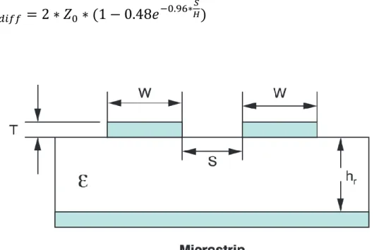
Fig. 3: A microstrip line over a dielectric layer spaced from a ground plane where H is the distance from ground or power, W and T is the width and the thickness of the microstrip line [8].
A microstrip transmission line is made up of a conductive line on top or on the bottom of the PCB, which is separated from the ground plane with an isolating substance. Because of the placement both air and the dielectric substance affect the impedance [9]. Too calculate the
characteristic impedance of an single ended signal with a copper trace we used equation (3) where ϵr is the PCBs dielectric constant, H is the
transmission lines distance to ground, W and T is the width and thickness of the transmission line [8].The answer is commonly measured in mils, but can also be represented in the SI derived unit microns.
√
(3)
The capacitance can be calculated with equation (4) and measured in farad per meter.
(4)
If a differential signals is used (See figure 4) the difference in impedance is calculated with equation (5) where Z0 is the characteristic impedance
of the traces and S is the space between the two transmission lines and
(5)
Fig. 4: A differential microstrip line over a dielectric layer spaced from a ground plane where hr is distance from ground or power, W and T is the width and the
thickness of the microstrip line and S is the spacing between the two transmission lines [10].
2.2.2 Stripline
Fig. 5: A symmetric transmission line between two layers of ground or power where W and T is the width and thickness of the etch, H is the distance from ground or
A stripline, unlike the microstrip cannot be placed on top or the bottom of a board, but has to be located between two ground planes which are connected. This means that the board has to consist of no less than three layers, this also leads to the isolation on the transmission lines becoming a lot better. Unlike the figure the transmission line does not have to be centered, but can be asymmetrically placed.
The asymmetric placed transmission lines impedance is given by equation (6) where ϵr is the PCBs dielectric constant, H is the smaller
distance from trace in dielectric substance to the ground plane and H1 is the larger distance from trace in dielectric substance to the other ground plane. T and W are the thickness and width of the trace. The capacitance propagation delay and inductance per unit length of the asymmetric placed is defined in equation (7), (8) and (9) calculated in and [12].
√
[
]
(6)
(7)
√
(8)
(9)
If the traces on the board are symmetrically placed towards the ground/power plane it gives us equation (10) and (11) [11].
√
[
]
(10)
(11)
If the stripline is a differential (see figure 6) the difference between the two signals is calculated with equation (12) where Z0 is the characteristic
impedance of the transmission lines, S is the spacing between the two traces and H is the distance from the trace to power/ground plane [13].
Fig. 6: A differential stripline symmetrically placed between two planes of ground or power where S is the spacing between the two transmission lines and b is the spacing between the two layers [10].
2.2.3 Angle (Bend)
When creating a connection between different components there are often a need for an angle. But a 90 degree angle in PCB will reflect a large amount of the signal back towards the source of the signal. That causes a lot of problems for high-speed signals, however according to page 305 in Johnson and Graham [3] right-angle bends can work for digital designs in speeds up to 2 Gbps . To prevent the extra capacitance the most common way is using “mitering”.
Fig. 8A: Shows the output of a length matched differential pair.
Fig. 8B: Shows the output of a differential pair where they are not length matched and the logic does not switch to zero at the same time causing a noise pulse to occur on the receiver.
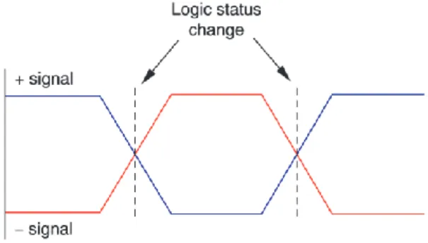
2.2.4 Length matched
For differential signals it is crucial that the logic goes to zero at the same time. That is a problem unless the transmission lines are length matched. If the differential signal is not length matched the logic that switches to zero will happen at different times and a noise pulse will occur on the receiver, see figure 8A and figure 8B [10].
2.2.5 Single-ended
A single-ended signal is a signal that uses one wire that has a shared reference and carries all voltages for one circuit to represent the signal. [3, p. 365] The main reasons for using it over differential signals is the lower cost and twice the number of inputs for the same size wiring connector. The disadvantages is that the input can suffer from noise picked up caused by the wire acting as an aerial [15].
2.2.6 Differential
A differential signal is a signal which sends current on two wires: the first wave carries the main signal and the second wave is provided for the flow of returning signal current. The voltages will not be opposite of each other but the current will be. This means that there is no need for a global reference voltage since the wires are references to each other. This also makes the system more reliant against disturbances provided the disturbance does not exceed the power-supply noise tolerance [3, p. 368-369].
2.3
Via
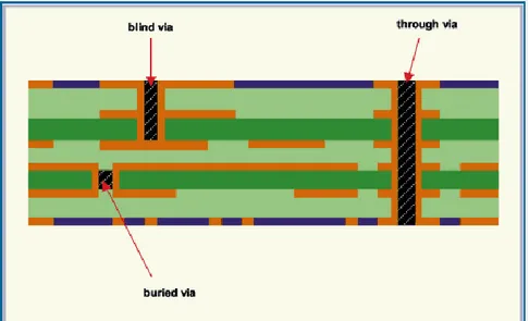
To connect one place on the PCB with another, going through the board is often required to do that. These plated holes are conductive and usually filled with copper-tungsten (CuW) for a low-resistance microwave grounding path, and offer high thermal conductivity [16]. A via consist of a barrel, a pad to connect the barrel with components or the trace and an antipad whose purpose it is to make sure that the via does not touch any unwanted connections [6, p. 102].
There are three different kinds of vias used in this thesis: Through hole via, blind via & buried via, see figure 9.
Figure 10 shows a thermal vias which is used for carrying away heat from power devices and will not be discussed further in this thesis.
Fig. 10: Shows how the thermal vias dispatches the heat from a component [18].
2.3.1 Blind via
A blind via is a via that does not go through the whole board. This creates more space inside the board for traces and can keep the bards dimensions smaller. The biggest downfall of a blind via and also the buried via is the cost and the time to make them [19].
2.3.2 Buried via
Buried vias is a hole that does not reach the top or the bottom board, which makes more space for components and traces.
2.3.3 Through hole via
The most common and least expensive is the through via. It goes as the name suggest through the whole board and can connect to any layer on the board. The simulations in this thesis have focused on filled plated-through vias since they are the most cost efficient and easiest to probe onto.
2.3.4 Stub
Fig. 11: A through via where the transmission line changes layer, creating a discontinuity because of the stub [20].
A stub is when a signal is going through a part of the via, see figure 11. This causes the rest of the via to conduct as a transmission line with significant degradation around its resonant frequency. To know where the degradation occurs we use the following formula for calculating the maximum stub length in inches is equation (13) where DKeff is the electric constant of the material around the via and BR is the bit rate [21]. The shorter a stub the further up in frequency the loss is pushed.
√
(13)
If the length of the stub is known we can calculate the fundamental frequency calculated in Ghz with equation (14) where Stub_len is the length of the stub in inches.
3
Methodology
During the analysis we used different methods and equipment which includes measurement on the PCB, Programming in Python and Matlab. We also calculated and measured amplitude, frequency and cross correlation towards each other to see the difference between the same samples but at different times.
3.1
Printed Circuit Board check
The first part of the thesis work was to test different examples of physi-cal boards provided to us by Ericsson. Too be able to answer what is required to implement the flying probe into the design process we were provided with PCB designs of three different examples of typical PCB design for Ericsson.
The layout of each PCBs was divided into different sections to make it easier to see where different components where located on each board and to find out where the larger components are most commonly found on each Ericsson PCB.
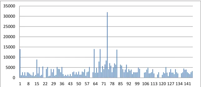
The names and exact height/location of significant components were extracted using the Allegro viewer and the components datasheet. This was entered into an excel sheet which was then used to find the average height of the relevant components. This allowed us to get an idea of how long the flying probes pogo pins have to be too not break any components while moving along the board. If the height was above the chosen threshold of 10 mm (this was chosen since it is higher than 90 percent of the placed components according to our measurements) for components we wrote down the height, section and name of the com-ponent so that we could instantly know where the highest and what kind of components that could endanger the probes fragile tips were located, see figure 28.
After this manual check of the height and location of relevant compo-nents was concluded we did another statistical analysis covering every single component on the board. This data was parsed from a text file that was extracted from the PCB package file provided and entered into another excel sheet. After collecting all the necessary data in excel, diagrams were made out of them showing the statistics of what kind of heights components have on different type of PCBs that are used by Ericsson. This said, only three different cards were tested and the results are to represent the cards from the Ericssons digital radio department and are not representative of Ericssons entire lineup.
Fig. 28: The different heights of significant components on one test board measured in micrometer, divided into sections with the back of the board starting at number 85.
3.2
Oscilloscope measurements
For measuring the signals from the three different PCBs a 15 gigahertz high-frequency oscilloscope was used. The signals we looked at were chosen based on how frequently they occurred as an output from the FPGA. The results from the oscilloscope were then extracted onto our computers and used to answer if the new probe is better than the old one using Matlab and Python code to calculating amplitude, frequency and rise time among others. We decided to import the information to Matlab and Python since the oscilloscope could not take multiple samples and therefore would not be able to show the results from the different probes. But it could be used to verify if the signals was close to the expected values.
The new probe will only be able to measure from almost directly above while the old one was handheld and could therefore use different angles. Our oscilloscope could not measure if the angle of the probe tip could change the outcome of the samples signals and if the outcome is different how much of a difference it is.
3.3
Programming
0 5000 10000 15000 20000 25000 30000 35000 1 8 15 22 29 36 43 50 57 64 71 78 85 92 99 106 113 120 127 134 1413.3.1 Python
Python was selected because it is an easy understandable programming language that is easy to further modify and with a lot of functions that fit our needs. It was used to format the results taken from the oscillo-scope since Matlab could not read the file that where written from the oscilloscope. This Python program picked and transferred the text string and put them in a way that Matlab could handle. This resulted that Python was only used for formatting the results to Matlab which then made the calculations and plots.
3.3.2 Matlab
The choice of math based program was very easy since Matlab was available to us and we had experience using similar math based pro-grams. It was also picked because it is a very good mathematic program with a lot of functions, easy maneuverable interface and a lot of online support.
Python first formatted the results from the oscilloscope into a text easy understandable for Matlab that was used to get frequency, amplitude among others and to cross-correlate the different signals. The results from each sample were then put into an excel arc so that the comparison between the similar signals taken from the new and old board could be compared. The code from Matlab was made to compare multiple different simulated or measured results and see if or what was the optimal distance to place an extra via in the signal path with the signal integrity in mind. This means that the code verified where a via simu-lated from ADS and HFSS could be placed. This was compared to the “ideal” case where no via were put in the signals path. The code was written in a way so anybody could easily select the signal they wanted to check on and see where a via is feasible to put in that design.
Unfortunately these measurements could not be done with the new board because we had to make many other changes to the board. All those changes made the two boards incomparable since the difference in the same signal might have to do with other changes than the extra via.
3.4
Simulation
In order to understand how placing a via in the signal path will affect signal integrity we chose to simulate rather than doing real world measurements because of repeatability and reliability of the results produced. The most extensive simulation used in this thesis was to see how an extra via and placement of that via in the signals path affected the signal integrity. The other smaller simulations were on how the changes in level and nearby vias affected the values. All simulations
were made using ADS and HFSS using the methodology explained below.
3.4.1 HFSS
HFSS is software designed for simulating 3D full-wave electromagnetic fields [23]. Within the scope of this thesis it is used for making different kind of designs to test if any are viable for manufacturing. To learn the basics of how to use HFSS we primarily used an Intel online education PowerPoint [24].
HFSS was used to answer the question of where a via could be placed in the signal path without disturbing the results of the signal, see figure 13. We also tested the electromagnetic fields to see where it is disrupting the sent signal. The design is made up of twenty layers of dielectric and copper, see figure 14. It is made with a single ended signal going a certain distance before reaching the first vias and then going another fixed distance to the “original” via. The vias are in these cases filled with copper and have a connection with the etch on the tenth layer and have a keep out distance so that it does not touch any other unwanted layer. The green vias are the ground vias and are not connected to the etch. On top we have a measuring point between the regular via and the ground via to create a connection to be measured on. There is also an “ideal” design where there is only one regular via and one ground via, why both were made is to see how an extra via in the signals path affect the integrity of the signal. This was tested since there is not always reasonable to measure the results at the receiving end because there is might be a component placed to close, and sometimes the signal can lose its integrity if the via is placed at the wrong distance.
The designs simulated signals ranged from zero to thirteen gigahertz to find the optimal placement for those vias so that the signal integrity would be mostly intact. This range is far bigger than the current signals Ericsson is using for these kinds of signals, but they wanted to make sure that the solution is viable for future use.
After simulating the different lengths of the vias the results were exported to ADS for further investigation and plotting.
Fig. 13: A pair of vias put at a specific distance from the other vias to measure the impact of an extra via.
Fig. 14: The buildup of our design in HFSS showing twenty layers of copper and FR4, a through ground via and a through via for the signal.
3.4.2 ADS
ADS is an electronic design automation software for RF, microwave, and high speed digital application [25]. We used it to simulate how our designs from HFSS worked if we would like to probe the results. Also how much influence the probes themselves have on the results of the signal. To get those results we simulated the structure in both the frequency and time spectrum (See appendix A for complete results from simulations).
Frequency Spectrum
Too be able to answer if the new probe is better than the old probe the equivalent circuit of 600A-At and D830 were created. They were created from LeCroys equivalent datasheet and used to see how an extra via would react to the different probes. Since we had to “create” the probes design either the whole circuit could be used or a component could be made that were equivalent to that design. The later was picked because of the simplicity of just seeing one component instead of the whole design, see figure 16. Both probes were used in the same design but not at the same time for comparison how different probes in general affect the end result. To test different frequencies an S-parameters sweeper was set to sweep from zero to thirteen gigahertz. First an “ideal” construction (without a via in the middle of the transmission line) was used, see figure 15. This construction was made out of two terminals with an impedance of 50 Ohms each to represent the loss of a real design and an S-parameter reader that had the values from the HFSS “ideal” design.
Fig. 15: A design from ADS measuring our ideal case in frequency, with the used information extracted from HFSS.
After the ideal construction, a construction to see where a via could be placed in the signal path without affecting the signal integrity was made. Too make such a design it had to have three measuring points (because of the extra via) instead of the two that was used in the “ideal”. Therefore an .s3p file was written instead of an .s2p. This made it a little more complex and the S-parameter reader had one more output that had to be addressed. On the third output the two probes and a very high resistance resistor were placed, though they were never simultaneously used, see figure 16. The simulation was made to answer the problem of where a via could be placed in the signal path and how the signals integrity would look like at the receiving end, how the different probes would affect the signal and how similar the signal would be to the original taken from a oscilloscope.
Fig. 16: A design from ADS measuring our non-ideal cases in frequency. It can be measured with two different probes or with a resistor with one Mega Ohm resistance, in this specific design we are using the 830 probe.
When the design was simulating, ADS checked if the design is acceptable and an output will be shown, that window plotted the difference between the ideal and in this figure the D820 probe, see figure 17. The plots are representing the difference from output to output while using zero to thirteen GHz and input to output where they are put in magnitude and decibel. The output found in figure 17 is only used in to see if the constructions behaved as expected. If the output was similar to the expected value an automatic saving function placed in ADS was used to save the results into a format that then was used in Matlab for more exact calculations.
Fig. 17: The frequency output we get from our ideal (red) and non-ideal (blue) when we measure the difference in output vs input and output vs output, measured in magnitude and decibel.
Time Domain
Like the frequency analysis the 600A-AT and D830 probe were used for measuring. The setup is similar but instead of the S-parameter sweeper a transient analysis going from zero to two nanoseconds with ten picoseconds intervals were implemented. To send the signal a voltage step generator with a specified rise time that represents the signal speed is going through a resistor to the two port s-parameter file opener. The resistor is set to the same resistance as the transmitter line would have, see figure 18.
The measurement is taken before and after the s-parameter file opener block in the design and then saved onto another file for further investigation in Matlab.
Too see where a via could be placed in the time domain and see how it affects the signal a design similar to the one used in “Frequency Spectrum” had to be used (explained more in “Frequency Spectrum”). Because the S-parameter file opener had to a three port instead of a two port an .s3p file instead of an .s2p file had to be made in HFSS. It is similar build as the frequency constructions but with a resistor instead of a terminal with a loss of 50 Ohms and a step generator, see figure 19. While simulating the results the output is checked and then plotted them to see if the results are plausible (see figure 20) before exporting them to Matlab for further investigation.
Fig. 19: The non-ideal time-domain design, able to test with two different probes or with a one resistor with one Mega Ohm resistance, in this specific design we are using the 830 probe while the 600 is inactivated.
Fig. 20: The output in time-domain where we get the ideal (red) and non-ideal (blue) in the first two and the two later measures difference when the measurement is taken from the “Probe” wire(red) and input/output(blue), all four outputs is measured in mV. For higher resolution picture see Appedix A.
4
Results
The results have been divided into two separate categories, simulation results and PCB measurement results.
4.1
Simulation Results
The simulations were made to see where a via could be placed in the signal path without affecting the signal path to much and also how different the two probes are to each other.
While creating the Matlab simulations we could see that the rise time of the plotted signals where very alike but started at different times (depending on location of the new via). The stub effect created from the extra via would also happen faster the closer the via is located to the transmitter, see see figure 21.
This may cause a problem depending on the frequency of the signal. If the frequency is low there will be no problem but a higher frequency will cause problems, see figure 23. In our case where the real single ended signals rarely reach any high frequency the stub effect will have almost no effect on the signal.
In the frequency spectrum the stub effect from the different lengths between the vias are more visible since the reflection of the signal occurs more often when the first via are close to the source, see figure 22. When taking the values and correlating them to see how they compare to the original signal we can see that when the vias are placed too close to each other the electromagnetic current will disrupt the signal. To see if a via could be placed in the signal path figure 23 is a good representative where the values of the different placed vias with a very high resistance is placed in the signals path compares to the ideal case, measured in percentage.
Fig. 22: The Matlab output difference between the ideal (blue) and the non-ideal (red) cases in the frequency domain. The “0.6x3.6" represents how far from the start the first via is placed and the second number tells how far to the next via, measured in cm. For higher resolution picture see Appedix A.
Fig. 23: Shows the difference in percentage of how similar the twelve outputs are compared to the ideal case at different frequencies (the numbers to the left is the frequencies in GHz) and length to the first via and the original via. It is color-coded in order to make the differences more clear. The green represents 95% similarity and above, yellow is 90% to 95% similarity and red everything below.
From this diagram we can see that if the frequency is below one to two gigahertz the difference in placement of the vias is at worst just below 99 percent similarity. This is good considering that most single ended signals does not become more that a couple of hundred megahertz. If the single ended signal has a higher frequency the length with the best average signal integrity was when the via was put four to five millimeters from the receiver, but different options are viable depending on the type signal. If a double ended signal is used, extra vias in the way are harder to place since the time span in when the signal can arrive to the vias is much lower and not to recommend.
Too see the difference between the new and old probe the same simulations as the previous one was conducted except that a probe was placed on the extra via, both had a dramatic negative effect on the resulting signal, but the old probe was better on the lower frequencies while the new was better overall. This concluded that a frequency higher than five gigahertz is not acceptable in most solutions and for many the five gigahertz can actually ruin the signals integrity too much. When using the probes and a high frequency signal the only placements usable enough is four to six millimeters away from the receiver, but the type of signal has to be considered amongst others. As in the previous chart within two gigahertz the placements does not matter since they are very similar, see figures 24 and 27.
If the results is coming from the perfect case most placements would be acceptable, but after seeing the effect of different probes we could see that most options are not that good. In this specific case the best average for all the frequencies was the four millimeters vias away from the original receiving via.
This displays that the results may differ a lot depending on what kind of probe or load that will be used or placed on the via pad. If the signals are under one gigahertz every placement will yield about the same results. If the signal is above a couple of gigahertz the best choice is to not have any vias in the way at all because the signal might have lost information on the way.
Fig. 24: shows the difference in percentage of how similar the twelve outputs are compared to the ideal case at different frequencies when measuring with an 830-probe (the numbers to the left is the frequencies in GHz) and length to the first via and the original via. It is color-coded in order to make the differences more clear. The green represents 95% similarity and above, yellow is 90% to 95% similarity and red everything below.
Fig. 27: shows the difference in percentage of how similar the twelve outputs are compared to the ideal case at different frequencies when measuring with a 600-probe (the numbers to the left is the frequencies in GHz) and length to the first via and the original via. It is color-coded in order to make the differences more clear. The green represents 95% similarity and above, yellow is 90% to 95% similarity and red everything below.
4.2
PCB Measurement Results
Too see what was required to implement a flying probe we began with measuring the components on the board so that the flying probe could pass over or around them without breaking either the probe or the component. The results displayed that the best option would be to place the bigger components on either the front or the back of the board, often the front as most big components are placed on top, shown in figure 28. This will make the changes on the board more expensive because of more components placed on the same area. The small changes we have made to the board already took a lot of time and work, from this we conclude that it would cost too much to re position components and implement different rules on an existing board and will therefor only be used when designing new boards. Too be able to measure the board with an automatic probe the vias will have to open, this means that the vias will have to be filled or have a plate on top of the hole. Also to be able to fit the extra ground vias the placement could be harder and blind and buried might have to be used more frequently which will increase the cost of the board.
We also had to find a couple of different vias that we could measure on and alter to be tested on the new board to see if an extra via would affect the integrity of the signal. These points were measured with an oscilloscope and the output was cross correlated to the newer signal. One of the current problems when testing a PCBs signals is the time taken to scratch the chosen vias. Too be able to implement the new flying probe system this problem could possibly be solved with an opening in the solder mask. The problem with that solution is that it may cause a short circuit on the board, but that risk is already apparent with the components legs being exposed which are not a big problem according to some of the Ericsson experts.
If a flying probe is to be used the vias cannot be placed anywhere and anyhow on the board so the vias has to be placed vertical or horizontal to the sides of the board with a ground via on a specified distance (as per the limitations of this specific flying-probe), this will inevitably lead to designs taking up more space on the board which answers our question if the board has to become bigger, as shown in example is figures 25 and 26. Before the start of this thesis the vias were put anywhere the designer thought it to be appropriate to be placed, but to be able to use a flying probe the horizontal or vertical rules have to be applied. As mentioned before the one problem with vias placed either horizontal or vertical is that every component will most likely take up more space than before, see figures 25 and 26. In the first figure almost all the vias are inside or close to the components outline, but in the new design there is not as many inside the components space because of the new design rules.
However the measured signals from the non-modified board and the modified was very similar to each other, but since we have changed quite a lot on figure 26 (except from the placement if the vias) the results are not compatible with each other because we cannot be sure that it is only the changes to the vias that have given us similar results to the original design. If we look at the simulated results we can see that the signals would be around 98 percent similarity.
5
Discussion
5.1
Simulations/Hardware
To know what is required of the design process to be able to implement an automated PCB testing system we first had to see how the flying probe would be able to move and test. From 3.1 we could see that the heights of certain components would be too great, which would cause the new probe to accidently bump into that component and break. The flying probe could also only measure vias placed vertical or horizontal to the board. This will as we can see in figure 26 make the components take up more space and require more ground vias.
The analysis of the differences between the new and old probe displayed that the simulations were quite similar, see figure 24 and 27. The differences were only a couple of percent, but the old probe was better at lower frequencies while the new probe had a better average. The new flying probe will also have a hard time measuring on PCBs with a lot of high components, where the old probe could almost measure everywhere and angles, as we explained above.
To get a grasp on how much time and money it would cost to change a PCB we altered one entire component following our design rules, the DDR2 (figure 26). This was our biggest change in the hardware, and the best visual representation of future rules to implement when using a flying probe. Also on top of the board the transmission lines generally became more exposed due to the increased distance between pins on the components. The via and the internal transmission lines were placed further apart to prevent crosstalk between the wires. These changes made the average length of a transmission line on this component increase by a couple of millimeters, but the upside is that the lines became better length matched to each other. From our perspective we do not think it is viable to implement our changes on existing designs but instead use it for future designs.
The PCBs will most likely become bigger because of more rules regarding placement of vias. This will as we answered earlier be more work for the designers because of more things to think about, like horizontal and vertical placements. But if the rules are used from the start of construction of a new PCB it might not take much more time than usual.
To be able to see where an extra via could be placed in the signals path, the simulations from 3.4 and 4.1 was used.
From the calculations in 4.1 we could see that depending on different things on top of the via as a probe could affect the end result with up to two percent on the lower and five percent on higher frequencies (These results are based on two different probes and changes to the vias resistance). By looking at the plot of the frequencies of the ideal compared to the extra via we could see that the closer the extra via comes to the transmitted signal the earlier the first “stub” will occur. This will result in a very fluctuating and bad result at all those dips which makes it an inferior choice unless the signal is in the MHz scale. If the extra via is placed too close to the original via, the electromagnetic current will disrupt the signal and degrade the results, which also means that the extra via should not be placed within four millimeters from the original via as we could see in figure 23.
5.2
Conclusions
The simulated results show that the higher the frequencies go the more difficult it will be to put in another via in the signal path, if the signal is a very important one a via in the path might even be disastrous to the integrity of the signal. If the signal information is not of critical im-portance, a via could be placed within six millimeters but not closer than three millimeters to the original via.
If our rules are implemented, some signals will need to have an extra via in the signal path. All single ended signals will also need a ground via which will take a lot of space and be more difficult to place. This will probably also make the circuit boards a bit larger, but if the rules are implemented from the beginning of a design this might not be a prob-lem. Also when a flying probe is used components cannot be placed anywhere, If the component is too high or placed to near the via the flying probe will not be able to take the measurements. The first of those issues could be solved by having most of the bigger components on one side of the board and measure on the other. The second problem must become a design rule where no via can be placed too close to the nearest component. This can be achieved by creating a keepout area in the design around vias that are going to be measured by flying probe.
5.3
Future Work
For future work one could make rules that all the vias must be placed either horizontal or vertical when a new PCB will be manufactured. Also a “keep out” distance from the vias to the components will be a requirement for probing with a flying probe, this can be attained by creating a component in the PCB design program with a specified keepout distance. Also more research can be conducted of real life scenarios on how the vias react to different signals and other traces on different levels.
The open vias is also something that would need a thorough investigation to determine if the risk is too high to have the via pads opened or if the risk comparable to just having the components pads opened.
Reference List
[1] Amateur Radio Station W5TXR, The Printed Circuit Board, 2012.
http://www.w5txr.net/The-Printed-Circuit-Board.html 2013-12-12
[2] Helmenstine, A.M, Table of Electrical Resistivity and Conductivity, 2013.
http://chemistry.about.com/od/moleculescompounds/a/Table-Of-Electrical-Resistivity-And-Conductivity.htm 2013-12-12
[3] Johnson, H., and Graham, M., High-Speed Signal Propagation Advanced Black
Magic, New Jersey, Prentice Hall, 2003.
[4] PCB Fabrication, PCB Fabrication Material, 2013.
http://www.pcbfabrication.com/PCB-fabrication/PCB_Material.asp 2013-12-12
[5] multi-cb, Copper balance, 2011.
http://www.multi-circuit-boards.eu/en/pcb-design-aid/copper-balance.html
2014-01-14
[6] Hall, S.H., Hall, G.W. and McCall, J.A., High-Speed Digital System Design A
Handbook Of Interconnect Theory and Design Practices., New York, John Wiley &
Sons, 2000.
[7] http://en.wikipedia.org/wiki/Characteristic_impedance 2014-01-16
[8] Analog Devices. Microstrip and Stripline Design, 2009.
http://www.analog.com/static/imported-files/tutorials/MT-094.pdf 2014-01-16
[9] Bitweenie. PCB Design Microstrip vs. Stripline, 2013.
http://www.bitweenie.com/listings/microstrip-vs-stripline/ 2014-01-16
[10] Texas Instruments. Considerations for PCB Layout and Impedance Matching
Design in Optical Modules, 2011.
http://www.ti.com/lit/an/slla311/slla311.pdf 2014-01-20
[11] Brooks, D, Signal Integrity Issues and Printed Circuit Board Design, New Jersey, Pearson Education, Inc, 2003.
[13] Asuni, N. PCB Impedance and Capacitance Calculator: Differential Stripline, 2004.
http://www.technick.net/public/code/cp_dpage.php?aiocp_dp=util_pcb_imp_s
tripline_diff 2014-01-21
[14] Microwaves101, Bends in transmission lines, 2007.
http://www.microwaves101.com/encyclopedia/mitered_bends.cfm 2014-01-22
[15] Wren, J, What Is The Difference Between Single Ended & Differential Inputs?, 2011.
http://blog.prosig.com/2011/02/15/what-is-the-difference-between-single-ended-differential-inputs/ 2014-01-22
[16] UltraSource, Plated Through-Holes and Filled Vias, 2013.
http://www.ultrasource.com/design-guidelines/plated-through-holes-and-filled-vias.html 2014-02-03
[17] University of Bolton, Design for Product Build: Supplementary: Vias, 2005.
http://www.ami.ac.uk/courses/ami4945_dpb/supplementary/fapo/ 2014-02-03
[18] Rako, P, PCB layout tips for thermal vias, 2013.
http://www.edn.com/electronics-blogs/the-workbench/4421218/PCB-layout-tips-for-thermal-vias 2014-02-03
[19] Kerek, N, Blind and Buried Vias.
http://www.omnicircuitboards.com/vias/ 2014-02-03
[20] Polaris Instruments, Signal integrity effects of vias, stubs and minimizing their
visibility, 2010.
http://www.polarinstruments.com/support/si/AP8166.html 2014-02-04
[21] Simonovich, B, PCB Vias- An Overview, 2011.
http://blog.lamsimenterprises.com/2011/02/15/pcb-vias-an-overview/
2014-02-03
[22] Bennett, P, Acculogic: Flying Probe Testing Overview, 2012.
http://www.smta.org/chapters/files/Arizona-Sonora_SMTA_Presentation_Nov13.pdf 2014-02-04
[23] Ansys, Ansys HFSS, 2013.
http://www.ansys.com/Products/Simulation+Technology/Electromagnetics/Sig
nal+Integrity/ANSYS+HFSS 2014-01-22
[24] USC, USC Signal Integrity Lab Course 2, 2005.
http://download.intel.com/education/highered/signal/ELCT762/class09.ppt
[25] Agilent Technologies, Advanced Design System (ADS), 2013.
http://www.home.agilent.com/en/pc-1297113/advanced-design-system-ads?
2014-01-22
[26] Teledyne Lecroy, Operator’s Manual WaveLink Series Differential Probe (4, 6
Ghz), 2013.
http://cdn.teledynelecroy.com/files/manuals/wl6g-om-e.pdf 2014-04-11
[27] Nexlogic, Flying Probe Test Ideal For Prototypes, 2012.
http://www.nexlogic.com/services/pcb-testing/flying-probe-testing.aspx
![Fig. 12: Picture showing an instance where a flying probe cannot get too close to a probing point if a tall device is too close [22]](https://thumb-eu.123doks.com/thumbv2/5dokorg/4249061.93766/13.892.165.619.107.463/picture-showing-instance-flying-probe-close-probing-device.webp)
![Fig. 1: the buildup of a symmetric PCB, made out of copper and FR4 [5].](https://thumb-eu.123doks.com/thumbv2/5dokorg/4249061.93766/15.892.156.350.682.868/fig-buildup-symmetric-pcb-copper-fr.webp)
![Fig. 2: The transmission line where I(x) is the current phasor and V(x) is the difference in voltage between both etches [7]](https://thumb-eu.123doks.com/thumbv2/5dokorg/4249061.93766/16.892.157.731.577.796/fig-transmission-line-current-phasor-difference-voltage-etches.webp)
![Fig. 3: A microstrip line over a dielectric layer spaced from a ground plane where H is the distance from ground or power, W and T is the width and the thickness of the microstrip line [8]](https://thumb-eu.123doks.com/thumbv2/5dokorg/4249061.93766/17.892.190.605.122.344/microstrip-dielectric-spaced-ground-distance-ground-thickness-microstrip.webp)
![Fig. 6: A differential stripline symmetrically placed between two planes of ground or power where S is the spacing between the two transmission lines and b is the spacing between the two layers [10]](https://thumb-eu.123doks.com/thumbv2/5dokorg/4249061.93766/20.892.170.674.136.344/differential-stripline-symmetrically-placed-planes-spacing-transmission-spacing.webp)
![Fig. 10: Shows how the thermal vias dispatches the heat from a component [18].](https://thumb-eu.123doks.com/thumbv2/5dokorg/4249061.93766/23.892.158.660.113.340/fig-shows-thermal-vias-dispatches-heat-component.webp)