AN AC HALL MEASUREMENT SYSTEM FOR HgCdTe
by Edith Creek
ARTHUR LAKES LIBRARY
COLORADO SCHOOL OF
MINES
All rights reserved INFORMATION TO ALL USERS
The qu ality of this repro d u ctio n is d e p e n d e n t upon the q u ality of the copy subm itted. In the unlikely e v e n t that the a u th o r did not send a c o m p le te m anuscript and there are missing pages, these will be note d . Also, if m aterial had to be rem oved,
a n o te will in d ica te the deletion.
uest
ProQuest 10783763Published by ProQuest LLC(2018). C op yrig ht of the Dissertation is held by the Author. All rights reserved.
This work is protected against unauthorized copying under Title 17, United States C o d e M icroform Edition © ProQuest LLC.
ProQuest LLC.
789 East Eisenhower Parkway P.O. Box 1346
A thesis submitted to the Faculty and the Board of Trustees of the Colorado School of Mines in partial fulfillment of the requirements for the degree of Master of Science (Physics).
Golden, Colorado Date Z / f - / m Signed: Edith Creek Approved: Dr. R. K. Ahrenkiel Thesis Advisor Golden, Colorado Date t / l i h 3 >r. John U. Trefny Tofessor and Head, 'Physics Department
A BSTRACT
A facility was designed and built to make ac resistivity and Hall voltage measurements on HgCdTe single crystal wafers. Soldering of electrical contacts to the samples was avoided by using indium coated, spring-loaded probes. Measurements were made using the van der Pauw technique. Resistivity (p), mobility (p.), and carrier concentration (n) were determined for several samples. Comparisons were made with existing dc data for the same samples. Resistivity measurements were found to be in good agreement (within 5%) but mobilities differed significantly (almost 2 0%).
iii
Table of Contents
Abstract...iii
List of Figures... v
List of Tables... . .vi
Acknowledgments... viii
Introduction... 1
Resistivity and Hall measurement... 1
The van der Pauw method...4
Infinite sheet method... 7
HgCdTe...8 Ohmic Contacts... 11 Measurement System... 15 Measurement Procedure... .18 dc Measurements... 21 Contact placement... 21
Carrier concentration, resistivity, and mobility... 25
Results and Discussion... 28
First tria l... 28
Verification of dc measurements...30
Second tria l... 31
Lockin amplifier. . . ... 31
Low current and low magnetic field te s t... 34
Error Analysis... 37
Conclusions... 39
References C ited... 40
Appendices A. Derivation of van der Pauw resistivity...41
B. Approximate errors in p and Rh ... 45
List of Figures
Figure Page
1. The Hall effect...2
2. Bar resistivity... 3
3. Contact placement for Rabcd and R b c d a ... 6
4. van der Pauw-Hall measurement... 7
5 FTIR transmission spectrum...10
6. Metal/semiconductor interface... 11
7. Forward and reverse biasing a metal/semiconductor interface... 12
8. I-V curves for a diode and ohmic contact... 13
9. Non-ohmic contacts on the sample... 13
10. Narrow deplection region at metal/semiconductor interface. ...14
11. Spring-loaded probes press into the side of sample. ... 15
12. van der Pauw-Hall measurement system... 17
13. Sample holder... .. ...20
14. dc resistivity measurements...35
15. dc mobility measurements... . .36
A1. Point contacts on an infinite half-plane... 41 A2. Graph of f(^ABCD.\ ...4 4
VRbcda I
List of Tables
Table Page
1. Contact placement test results... 2 2
2. Results of first tria l... 29
3. Verification of dc measurements... 30
4. Results of second tria l... 33
5. Low current and low magnetic field results... 34
Acknowledg ments
I would like my advisor, Richard Ahrenkiel of the National Renewable Energy Laboratory (formerly SERI) and the members of my thesis committee Thomas Furtak and Don Williamson for their help and support.
Special thanks to my husband John and my children Tracy, Wendy, and Kelly for their encouragement and patience.
Introduction
Resistivity, mobility, and carrier concentration are important in semiconductor research and manufacture. The Hall effect is a well-known phenomenon that is used in obtaining carrier concentration (n or p) as well as mobility (p) for a given material (1-4).
In 1958 L. J. van der Pauw described a technique for making resistivity and Hall measurements on planar samples of arbitrary shape. He derived an equation for resistivity which depends on two resistances and a transcendental equation involving the ratio of those resistances. The samples must be free of mechanical holes. Four ohmic contacts must be made on the periphery of the sample in order to make the measurement.
NREL has provided Colorado Research Laboratory with resistivity, mobility, and carrier concentration measurements on HgCdTe which the latter is developing for use in infrared sensors. An ac measurement system dedicated to HgCdTe has been developed.
Resistivity and Hall measurement. The carrier concentration (n or p) is obtained by making a Hall measurement on a sample. When current is passed through a sample in the x- direction (Figure 1) in the presence of a magnetic field in the z-direction, a voltage builds up in the y-direction. This voltage is a result of the Lorentz force on the carriers (positive or negative charges) as they move through a magnetic field.
Lorentz force F = q(E + v X B ) where v is the velocity of the charge carriers and B is the applied magnetic field.
The carriers are deflected in the y-direction until they build up an opposing E field so that the total force in the y-direction is zero and E y = v x B*.
|
i.
u
|
current
Figure 1. The Hall effect. Electrons moving through a sample in the positive x-
direction (current is in the negative x-direction) in the presence of a magnetic field in the z-direction experience a force in the y-direction.
One can measure the voltage V (V=E/w), and current density J (J = l/wd = nev). One can derive an expression in which the only unknown is the carrier concentration
I B
n = x---- — . If the sign of the voltage is negative the charge carriers are electrons (n),
V y e d
if the sign is positive the charge carriers are holes (p) (1).
If one makes a measurement to determine the resistivity (p) of the sample, the carrier mobility (p) can be obtained from the relationship p = 1/nep. If the sample being investigated is a bar, then resistivity measurements can be made directly by measuring the voltage at two points along the bar in line with the known current (Figure 2). Using Ohm's law,
—* —* P
J = a E = ^ the resistivity is easy to obtain: _ Vab
p =E=_L_
P
J
i _
wd
current I
At low temperatures, the voltage contacts can have very high resistances. Bridge shaped samples, with large contact areas, have been used to get around this problem. It is often a delicate task to cut these samples. Van der Pauw (2,3,4) developed his technique for arbitrary shapes to avoid cutting the brittle semiconductor material. His method is used in the system described in this paper.
The van der Pauw method. In the van der Pauw method (2) four ohmic contacts are made on the periphery of the sample. A known current is driven from A to B and the voltage between C and D is measured. A transverse resistance is defined: Rabcd=
i AB (Figure 3a).
Next a current is sent from D to A and the voltage BC is measured. A second _ V a- V d
transverse resistance is defined: k bcda- — (Figure 3b).
The resistivity is given by p = iL d /^ABCD + Rb c d a| f where f satisfies the
In 2v
2
'
The derivation of these
relationships is given in Appendix A. The important assumptions here is that point contacts be placed on the periphery of the sample. Errors worked out by van der Pauw for contacts that do not meet these requirements are given in Appendix B.
For the Hall voltage measurement on a sample of arbitrary shape, current is sent through contacts at B and D and the voltage AC is measured (Figure 4). The voltage, in zero
only the added component of the electric field in the y-direction in the presence of a magnetic field that we are interested in, we must subtract the zero field value of the voltage. The Hall
T> B
equation for carrier concentration (n) becomes n = — r or n = — r —
Figure 4. Contact placement for van der Pauw-Hall measurement.
Infinite sheet method. Another method of making Hall and resistivity measurements was described by Lange (5) in which the contacts are placed near the center of the sample. The contact spacing must be small compared to the size of the sample. For the resistivity measurement the contacts must be arranged in a circle, for the Hall measurement any
arrangement except a straight line is permitted. The measurements themselves are carried out as described by van der Pauw, but the resulting resistivity p is twice the van der Pauw value:
Poo sheet = ^ Pvan der Pauw
The mobility also has the same factor of two: Mh ~ sheet= 2 |Xvan der Pauw
The van der Pauw technique was selected instead of the infinite sheet method due to the small size of the samples we were studying.
HaCdTe
The measurement system described in this paper has been designed to make resistivity and Hall measurements on HgCdTe, a material that is currently receiving a lot of attention for use in
infrared sensors. Hg(1x)CdxTe is a ll-VI ternary alloy semiconductor with a zinc-blende
structure. It is a direct gap material; the energy gap can be varied from E = 0 at x = .15 up y
to Eg = 1.6 e V f o r x = 1 (6).
The energy gap as a function of temperature and mole fraction of Cd (x) has been experimentally determined by Schmidt and Stelzer (7):
E = - .25 + 1.59x + (5.233 X 10'4) T (1 - 2.08x) + ,327x3 y
and also by Hansen, Schmidt, and Casselman (8);
E = -.302 + .193x + (5.35 X 10'4) T (1 - 2x) -.81 Ox2 + .832x3
y
Ideally, an intrinsic (undoped) material will have transitions only between the valence band and the conduction band. Since there are no shallow impurity levels added by doping, conductivity will be produced only by photons with energy of Eg or greater. The electronic current can be monitored to determine the intensity of incoming photons. If the material is cooled to liquid nitrogen temperature, thermal excitations of electron-hole pairs and the related background currents are reduced. This is the general idea behind the infra-red sensors that are based on HgCdTe.
The measurements discussed in this paper were made on HgCdTe single crystal wafers that were provided by Colorado Research Laboratory (CRL) in Walsenburg, Colorado. The samples were either 8mm or 10mm in diameter and varied from approximately .5mm to 1mm in
were intrinsic n-type, n on the order of 1015 or 1016. The band gap at liquid nitrogen and
room temperature for these HgCdTe samples is (using the equation from reference 7 above): Eg (77K, x=.2 2) = .12 eV
Eg(300K, x=.22) = .18 eV
These bandgaps correspond roughly to a maximum wavelength of 10pm (.12eV) and 7pm (.18eV) where A.(pm) = 1.24/E (eV). These are infrared wavelengths (the range of visible light is .7pm to .4pm). This means that the lowest photon energy that will excite an electron- hole pair in this material is .12eV if the HgCdTe is at liquid nitrogen temperature.
An FTIR transmission spectrum (Figure 5) was made for sample 1263-J on the Digital FTS-40 system at the School of Mines. The spectrum is plotted as percent transmission versus wavenumber in inverse centimeters. Wavelength (X) in microns is obtained by inverting the wavenumber and converting to microns. For example, 1000 wavenumbers is 1000/cm. Wavelength is then .001 cm = 10 pm. Higher wavenumbers correspond to higher energies. This spectrum shows absorption starting at about 1100 wavenumbers (.14eV) and continuing up to 4000 wavenumbers (.49eV) . From calculations of the badndgap, absorption is expected starting at about .18eV, so this is a reasonable result. There is a decline in transmission below about 500 wavenumbers (.06eV). This is probably due to the Reststrahlen or the lattice absorption of infrared radiation producing optical phonons.
o
CO CM
ID
UOjSSjUJSUBJJL %
Figure 5. FTIR transmission spectrum of sample 1263-J.
4 0 0 0 3 5 0 0 3 0 0 0 2 5 0 0 2 0 0 0 1 5 0 0 1 0 0 0 5 0 0 34
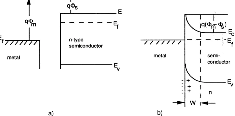
In order to make resistivity and voltage measurements, ohmic contacts must be made on the HgCdTe samples. When a metal, such as the gold wire used for the electrical leads, comes in contact with a semiconductor such as HgCdTe, the resulting metal/semiconductor interface presents a barrier to charge flow called a Schottky barrier. This barrier forms on contact to equalize the Fermi levels in the two materials. Constancy of the Fermi levels is a condition of thermodynamic equilibrium. Figure 6a shows a metal and semiconductor with
qc|)m
greaterthan
q<|)s.
When the metal and semiconductor are brought into contact, the Fermi levels(Ef)
must align as in Figure 6b.
m
E
f7777777
n-typesemiconductor/ / / / / / /
E
fmetal metal semi
conductor
E
v + nW
a)
b)
Figure 6. a) metal and semiconductor Fermi levels
(Ef)
are different with respect tothe vacuum level, b) Fermi levels must align at an equilibrium value when metal and semiconductor are in contact.
In this case electrons from the semiconductor flow to the metal until equilibrium is reached (1). A depletion region (W) forms within the semiconductor due to this charge flow. The
structure is called a Schottky diode owing to the asymmetry of current flow. When a diode is forward biased (Figure 7a), the barrier is small and electrons flow from the semiconductor to the metal (current flow is from the metal to the semiconductor).
+ V
-/ -/ -/ -/ -/ -/ -/
metal- V +
_ _
-C Ef semi conductora)
/ / / / / / /
metal semi conductorFigure 7. a) metal/semiconductor forward biased so that barrier height is lowered and current flow is not restricted, b) reverse biasing prevents current flow.
When a diode is reversed biased (Figure 7b), the barrier height is increased and almost no current flows. The resulting current-voltage (l-V) curve is very different from that of an ohmic contact (Figure 8).
Figure 8. a) l-V curve for a diode, b) l-V curve for an ohmic contact.
J
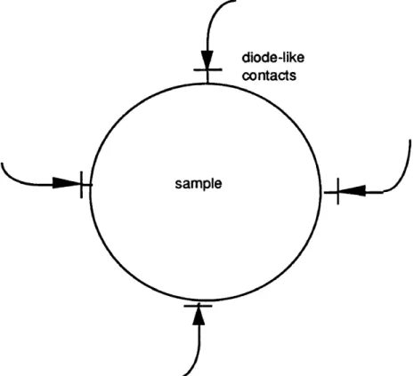
Figure 9. The sample with non-ohmic electrical contacts. diode-like
contacts
These diode-like electrical contacts affect electrical measurements that we are trying to make (Figure 9). In order to make ohmic contact, an indium solder is applied to the contact region of the semiconductor sample. The indium diffuses into the HgCdTe and heavily dopes the surface region n-type. A heavily doped Schottky diode has near ohmic behavior due to the small width of the junction. The junction conducts by tunneling in reverse bias and the resistance to current flow is small. It is not necessary to solder the indium in order to achieve this effect. It is sufficient to coat the electrical probe with indium and just press it against the HgCdTe sample.
/ / / / / / /
“ -E
f metal semi conductor + +n
Figure 10. Charge can easily tunnel through the narrow depletion region that is created when the surface is doped n-type.
ARTHUR LAKES UBRNW COLORADO SCHOOL OF M IN II
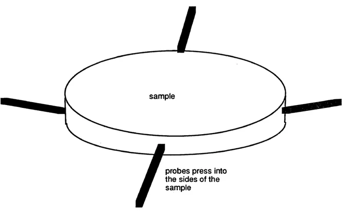
In order to keep the electrical contacts to the sample as small and as close to the edge of the material as possible as required for the van der Pauw technique, the sample holder was designed to use spring-loaded contacts aligned to make contact with the side of the sample (Figure 11). Since the probes press against the sample, no soldering to the sample is necessary and therefore the processing is simplified.
sample
probes press into the sides of the sample
Each probe is mounted in a copper rod which is held in place along with the sample in a teflon holder. The placement of the contacts is therefore flixed at the same position for every sample. In order to make an ohmic contact with HgCdTe, the probe tip must be coated with indium solder. Several samples can be measured before the solder needs to be replenished.
One shielded wire was connected to each copper rod and then through a BNC
connector to a switching box. This allows the current input and voltage readout to be made under computer control (see Figure 12 and 13). An 800 Hz, 2mA ac current is supplied to the sample by an EG&G model 5210 lockin amplifier. The lock-in amplifier detects the differential voltage between two leads. As the lockin amplifier is a very narrow bandwidth amplifier, only the 800 Hz ac signal is amplified. This helps eliminate electronic noise from the measurement. The EG&G 5210 does not have a current source. It has a voltage source which is connected to a 100 ohm resistor which is placed in series with the sample. This serves as a constant current source which changes very little with the sample resistance. To improve accuracy, the voltage across this resistor is read (and divided by 1 0 0) to get the true current for each
reading taken. It is cannot be assumed that this current stays constant.
The sample holder with attached leads is held between the faces of an electromagnet in a fixed position. It can also be locked into a fixed position above the magnet so that
measurements at zero magnetic field can be made without the influence of the residual field (about 50 gauss) of the electromagnet.
The magnet is powered by an Electrostatics, Inc. 50 volt 6 amp dc power supply model
LS50. It is operated at approximately 45 volts and 4 amps and produces a field of 2
kilogauss. A hand-held gaussmeter is used to check the field. Each time the magnet is turned on it is adjusted to bring the field to 2 kilogauss (or kiloOersted).
A cup for liquid nitrogen has been made from a 3 inch nylon rod and cut to fit exactly between the faces of the magnet. The entire sample holder is placed in this cup and filled with liquid nitrogen for the low temperature measurement. It is allowed to evaporate when the measurement is completed. lockin amplifier Am sample voltmeter dc current source for magnet computer switching boxes current differential voltage
magnet and sample holder
Measurement ..Procedure
Before the measurement procedure is started, the sample must be placed in the holder and electrical contact made with the pogo probes. The probes are pushed into the side of the sample one at a time and a screw is tightened to hold each probe in position (see Figure 13). Contact between all combinations of two probes must be checked for continuity with an ohmmeter. The resistances for the HgCdTe samples we are studying are on the order of 5 ohms between any two contacts. Frequently poor electrical contact will be made and the resistance is on the order of 100 ohms between two of the contacts. The current still flows through the sample, but the contact resistance is too large compared to the sample
resistance. The values obtained for resistivity and mobility are incorrect. The solution to this poor contact problem is to adjust the pressure of the probes into the side of the sample. It may also be necessary to recoat the probe tips with indium. The use of spring-loaded probes helps because they eliminate the variable size and placement of the contacts that occurs when electrical contacts are soldered to the sample. However, spring-loading creates electrical contacts that are extremely sensitive and still somewhat difficult to make. Care in making these connections is the most critical step in the measurement process.
When a measurement is made, the following steps are done under computer control. 1. Current is input at A and B is grounded. The lockin amplifier is turned on and the ac
y n_ y A voltage across D and C is read. A resistance is defined: Rabcd= —7— —
ABC
2. Current is input at B and C is grounded. The amplifier is connected across A and D Va- V n
and the ac voltage is read. A resistance is defined: Rbcda= —4 — — Ibc
4. p (£2-cm) is calculated using the van der Pauw equation: p = ft d I R a b c d + R b c d a j ^
In 2'
2
/
5. Current is input at A and C is grounded. The lockin amplifier reads the ac voltage across B and D. Zero field resistance is defined: R (B = 0) =
Ia c
6. The sample holder is lowered between the faces of the magnet. The magnet is turned
on. The gaussmeter is used to check the field and the power supply is adjusted so that the magnetic field is 2 kilogauss. This is done manually and not by computer control.
7. With the current input at A, the ac voltage across B and D is read. Another resistance is defined: R (B ) = ^ £2 .
Ia c
8. The magnet is turned off.
.. _ d [R (B ) - R (B =0)] 1010
9. The mobility is calculated using the equation M* - where d is
the sample thickness in meters, B is the magnetic field in gauss, and p is the calculated value from step 4. The hybrid units of mobility are cm2/V-sec.
10. Carrier concentration is calculated n = 7 ^ 7 7 where e is the electronic charge
r cr (1.6 X 10' 1 9 Coulombs). The units of n are cm'3.
BNC cable
Pogo probes
Teflon stage
Test sam ple
tic Measurements
Contact placement. Before the ac system was built, a series of tests were made on one circular sample (#12-1107-A, 10 mm in diameter, .787 mm thick) to develop an understanding of the problems caused by varying contact placements. Van der Pauw discusses the errors in p and Rh due to a finite size of the contacts (as opposed to point contacts). He also
discusses the errors if the contacts are not exactly at the edge of the sample but placed a finite distance from the edge. A table of the these errors is presented in Appendix B. The tests were not an attempt to study the size dependence of the contacts, but only the placement. The existing dc Hall system at NREL was used for these tests.
Contacts were made by pressing a slice of indium wire about (.5 mm in diameter and about .2 mm to .3 mm in thickness) onto the top of the sample. If one side of the sample was more polished than the other, the more polished side was used for the electrical connections. A one inch piece of gold wire was the pressed onto this and held with tweezers. A good electrical contact was made by just touching the indium and gold wire lightly with a hot soldering iron. All the contact sizes were on the order of .1 mm in diameter and looked similar to visual inspection. The sample was then held in place on the sample holder by a non conducting paste. The ends of the gold wire leads were soldered to the connections on the sample holder and a curve tracer was used to make sure that the contacts were ohmic. Resistivity and Hall measurements were made with a current of 80 mA at room temperature and a magnetic field (for the Hall measurement) of 5 kilogauss. The contacts were removed after each measurement and discarded, new contacts were placed in different positions on the same sample for the next measurement. The results are given in Table 1.
Table 1 n (cm- L u (cm */V-sec) p mm J6 -2 4 .3 6 x 1 0 10548 1.36x 10 no solder mm 2.77 x101 7 2598 8 .6 9 x 1 0 -3 with solder mm 17 -3 3 .1 0 x 1 0 2348 8 .5 8 x 1 0 16 - 2 3 .8 3 x 1 0 11564 1.41 x10
n (cm—1 li (cm^/V-sec) p (O-cm ) 16 - 2 3 .8 8 x 1 0 11674 1.38x10 4.41 x101 6 9880 1.43x10 -2 1mm 1mm 4.94 x 101 6 9581 1.32x10 -2
In tests 4, 5, and 6 contacts were made only on the periphery, although the
configurations are quite different. We would expect that given equal contact sizes, the results would also be equivalent because the there is no offset from the edge for any of these
the results differ by only a few percent. Test 6 has the contacts placed in a very unsymmetric
configuration and the results differ significantly from 5 and 6 in carrier concentration and
mobility, but not in resistivity.
If 4 is used as the basis for comparison (since it is the most ideal), then from the error equations given by van der Pauw (see Appendix B), we would expect that test 1 would have a resistivity of about 1.40 x 10"2 Q-cm because one contact is placed 1mm from the edge.
We also expect the carrier concentration to be about 4.09 x 101 6 cm"3 for the same reason.
For test 7 in which the errors should be twice as large because two contacts are placed 1 mm from the edge, we expect the resistivity to be about 1.39 x 10- 2 £2-cm and the carrier
concentration to be 4.39 x 10¹⁶. The measurements are 5-10% larger than these predicted values. The conclusions from these observations is that the measurements are quite sensitive to contact placement. It is difficult to accurately predict the size of the error under the given conditions. No consideration was given to the finite size of the contacts or the fact the the sample properties may have changed due to the amount of soldering done on the sample, although both may have had significant effects.
Koon, Bahl, and Duncan (9) studied the contact placement errors using the van der Pauw technique on samples similar to ours and concluded that the approximate error formula given by van der Pauw was good only for low values of d/D, (placement distance from the edge)/(diameter of the sample). For values larger than d/D « .1, they found that the exact solution gave a much better fit for their data. The exact solution is given by:
In 1 +
Using this equation, I expect the resistivity in test 1 to be 1.39 x 10' 2 £2-cm, only slightly
less than the resistivity obtained using the approximate error formula. In test 7, I expect a resistivity of 1.38 x 10' 2 £2-cm. For contacts that are very close to the edge with d/D less
than .1, the approximate error formula give results that are essentially the same as the exact
formula. The experimental results I have obtained show much greater errors than either formula predicts.
It is interesting to note that contact size was not given much consideration in Koon's paper: there was just a statement that the leads were small. I chose not to investigate the errors due to contact size only because of the great difficulty in controlling this parameter. Although the van der Pauw error formula for finite size contacts leads me to believe that the effect is much smaller than that of placement error (see Appendix B), this needs to be
investigated experimentally. Koon states that they did not study the Hall coefficient because of the difficulty of preparing a homogeneous magnetic field for macroscopic samples.
Tests 2 and 3 demonstrate that for contacts placed in the center of the sample about 3 mm apart, the infinite sheet method is not valid. Both resistivity and concentration should have been twice the van der Pauw value, but 3 mm spacing is not really small compared to the
1 0 mm diameter of the sample, so the condition for the infinite sheet method is not met.
Carrier concentration, resistivity, and mobility. The Fermi-Dirac distribution function, f(E ) = p I + e(E-Ef)/kT_ describes the distribution of carriers in a semiconductor. The
concentration of carriers (n) that occupy the conduction band in an n-type material is given
f(E ) N(E) dE where N(E) dE is the density of states in the energy range dE. We
so that n = N c f(E c) (1). This leads to n = ---— ---« N c e-(Ec-Ef)/kT where N c also 1 + e(Ec-Ef)/kT
depends on temperature (N c a T 3/2). The intrinsic concentration ( nO is given by
ni = V N cN v e-^s/kT) where N c and N v are both proportional to T3 / 2 (N c refers to the
conduction band, N v refers to the valence band). ni is then given by n i= A T3 / 2 e^Eg/kT).
When intrinsic conductivity dominates, n = p = A T3 / 2 e-(Es/kT) The carrier concentration n,
when | i n is greater than Up, is one of the values determined from our Hall effect
measurements. From the expressions above, one expects n to be exponentially dependent on temperature with larger n for higher temperatures. Since the bandgap of HgCdTe is small, the intrinsic carriers, which are responsible for conduction at room temperature, are frozen out at liquid nitrogen temperatures. The carriers at low temperatures are due to extrinsic impurities in the material. This explains why there are more carriers at low temperatures than would be expected based on an exponential dependence alone. In particular, samples 1264-E and 1265-J (Table 2, dc measurements) have n - 2.5 x 101® at room temperature (300K) and n ~ 3.4 x 1 0 ^ at liquid nitrogen temperature (77K). The factor of 100 difference in these two values is typical of the HgCdTe data collected over a six-month period using the dc system at NREL.
Since the number of electrons thermally excited into the conduction band is exponentially dependent on temperature, the electrical resistivity of the material should be a decreasing function of temperature just due to the number of carriers present (11). The measured
resistivities of the samples 1264-E and 1265-J are p ~ .023 at room temperature and p - .17 at liquid nitrogen temperature, which agrees with the expectation.
Mobility is an important quantity in semiconductor characterization because it describes
c m 2 cm/sec
which is —--- :—rr-rr. Scattering mechanisms influence the mobility of charge carriers in a electric field
semiconductor. At high temperatures lattice vibrations, or phonons, dominate the scattering of carriers and reduce the mobility. As the temperature is lowered, phonon scattering
decreases and other mechanisms may dominate. Since the thermal velocity varies as T 1/2, the cross-section for ionized donor (or coulomb scattering) is greater at lower temperatures. Impurity scattering may dominate as the temperature is lowered. This includes intentionally added donors and acceptors. Also, unwanted, residual impurities may contribute to the scattering mechanism. Both neutral and ionized impurities (for neutral impurity scattering) may be involved. Mobility is proportional to T"3 / 2 for phonon scattering (at high
temperatures) and T3 ^2 for impurity scattering (at low temperatures) (1). The mobilities we
have observed in HgCdTe at room temperature are on the order of 104 . In contrast, the mobilities at liquid nitrogen temperature are on the order of 1 0® and have been recorded as
high as 2 x 10®. The main reason for the high mobility observed at liquid nitrogen temperature is the reduction of phonon scattering. The room temperature mobility is dominated by phonon scattering and the liquid nitrogen temperature mobility is limited by impurity scattering.
Results and Discussion
First trial. The first set of data presented in Table 2 was made manually on the new ac system and the value of f was taken to be 1 . 0 0 for the resistivity calculation (it was actually
larger than .99 for this data). The new data is compared with measurements that were made at an earlier time on the existing dc system at NR EL.
The range of measurements at liquid nitrogen temperature for the first sample, 1262-1, indicated something was wrong. The resistance measurements R a b c d and R b c d a differed by a factor of 1000 when they should have been close to the same, and R(B=0) and R(B=2kG) were about the same but were expected to be different by a factor of 50 at this temperature. When the sample was allowed to warm up to room temperature, it was found to be cracked into two pieces, although still held tightly in the sample holder. We were able to make the voltage measurements because the sample was still conducting, but the condition that there be no holes or discontinuities in the sample was violated and thus we could not apply van der Pauw's theorem to extract resistivity and mobility information.
sample 1262-1 d=.77mm 1264-E d=.77mm Table 2 ac measurements dc measurements 300K 77K 300K 77K p 2 . 2 0 x 1 0 ‘ 2 p 10343 n 2.75 x 101 6 2.17 x 10"2 10148 2.84 x 101 6 p 2.23 x 10“2 p. 11500 n 2.43 x 1 01 6 1.89 x 10‘ 1 106000 3.12 x 101 4 2.29 x 10’ 2 10809 2.53 x 101 6 1 . 8 6 x 1 0 ' 1 96492 3.48 x 101 4 1 265 -J p 2.28 x 10' 2 1.57 x 10‘ 1 2.25 x 10’ 2 1.54 x 10' 1 d=.90mm \l 10300 124000 10900 122883 n 2.66 x 101 6 3.21 x 101 4 2.54 x 101 6 3.30 x 101 4
The room temperature resistivity measurements agree quite well with the values obtained using the dc system. The largest difference was 2.6% for sample 1264-E. At liquid nitrogen temperature, the differences were as large as 1 0% for the same sample.
Verification of dc measurements. After comparing the data, the dc measurements were repeated to see if they could be duplicated. Sample 1262-1 was not used since it was broken. Samples 1264-E and 1265-J turned out to be p-type, which meant that there was a surface layer on the samples that was being measured instead of the bulk material. The indium/gold wire contacts were removed from the samples. A 3% solution of bromine in methanol
(Br/CHgOH) was prepared and the samples etched for about 30 seconds. Since there was still some indium on the surface of the samples after the etch, the new indium/gold wire connections were placed at different locations around the circumference. The dc
measurements were repeated at room temperature and are listed in Table 3. The resistivities are within 3%, the mobilities within 7% of the earlier dc measurements.
i s m s dc measurements 300K 1264-E p 2 . 2 2 x 1 O' 2 \l 10057 n 2.80 x 1 0 1 6 1265-J p 2.20 x 10' 2 \l 10435 n 2.72 x 101 6
Second trial. Three new samples were selected. These samples had been measured earlier on the dc system and still had the indium/gold wire contacts intact. These contacts were used and the dc room temperature measurements were made a second time. Two data sets were reproduced to within .5%, the third data set for sample 1262-A was significantly different from the original. Since the same leads were used, it is expected that the data be
reproducable to within .5%. After the dc measurements were performed, the leads were removed and the samples mounted in the ac system and measurements were made. The data in Table 4 includes both dc data sets along with the ac data. The resistivities obtained from the ac measurements agree very well with those from the dc measurements. The mobilities do not. Furthermore, it was discovered after the measurements had been made on sample 1264-1 (Table 4) that the lock-in amplifier was not being set correctly for the mobility
measurements and as a result, all mobility measurements including 1264-1 were incorrect. The resistivity measurements up to this point were not affected.
Lock-in amplifier. When the resistivity measurements are made, the current source from the lock-in amplifier is connected to the sample leads and the amplifier is set to maximize the detected signal. The phase of this detected signal is set to zero degrees, there is no out of phase component to this signal. When the second resistivity reading is made, the amplifier is reset to again lock in on the maximum signal. This is the correct procedure because the current is going through a different path for the second reading.
However, when the Hall measurements are made, the current path doesn’t change. In this case, the amplifier was locked in and the signal maximized when the magnetic field was zero. When the magnetic field was turned on, the electrical connections remained the same but the lockin was still reset. This is the source of the error. The lockin should not have been
reset at this step. In the presence of the magnetic field there is a Hall voltage detected that is the same phase as the zero field voltage. There is also a voltage detected that is 90 degrees out of phase with the zero field voltage (8). It is due to inductive pickup in the sample. If the
lockin is reset, this inductive voltage will be averaged with the Hall voltage to again maximize the signal and give an incorrect result. Due to this error, the mobilites in Table 1 and Table 2 are wrong along with the mobility for the first sample in Table 4 (1264-1). The resistivities are correct for these samples.
For samples 1265-F and 1262-A in Table 4, the ac resistivies agree to better than .5% wtih the dc resisitivities. The mobilities obtained from the ac measurements are as much as
17% higher than the dc values. In these two cases the mobility values were obtained by correctly keeping only the in-phase Hall voltage when the magnetic field was applied. In addition, the magnetic field was reversed and another in-phase Hall voltage reading was made. The zero field value was subtracted from each Hail voltage and the two values were averaged to eliminate magnetoresistance effects.
1264-1 d=.74mm 1265-F d=.8 8mm 1 2 6 2 -A d=.87mm Table 4 ac measurements 300K p 2.27 x 1(T2 \i 10904 n 2.53 x 1 01 6 dc measurements 300K original 2.27 x 10' 2 10438 2.64 x 101 6 recheck 2.28 x 1 0 - 2 10409 2.63 x 101 6 P P 2.23 x 10' 2 2.22 x 10' 2 2.22 x 10' 2 \i 12144 10415 10406 n 2.31 x 101 6 2.70 x 101 6 2.71 x 101 6 2.25 x 10"2 2.34 x 10‘ 2 2.25 x 10' 2 ]l 11832 11290 10612 n 2.35 x 101 6 2.37 x 101 6 2.62 x 101 6
Low current and low magnetic field test. The dc measurements were routinely made with an 80 milliamp current and 5 kilogauss magnetic field. Equipment limitations require that the ac measurements be made with a 2 milliamp current and 2 kilogauss magnetic field. A series of dc measurements were made for similar low current and low magnetic field to check these differences as a source of error. The measurements were made on sample 1264-D and results are presented in Figures 14 and 15. The ac results are presented in Table 5. The average of the dc resistivities measurements is
2.22 x 10' 2 £2-cm, the ac measurement is within 5% of this value. The ac mobility
/ o
measurement is 12% higher than 10445 cnTvV-sec, the dc average.
Table 5 -a c measurements dc average 300K 300K 1264-D p 2.33 x 10' 2 2 . 2 2 x 1 0 ' 2 d=.84mm p. 11708 10445 n 2.29 x 1 01 6 2.70 x 101 6 C0L0R® 0 GOIO^.C
R e s is ti v it y 0.025 0.024 0.023 0.022 0.021 0.020 0.019 0.018 0.017 0.016 0.015 .1 1 10 1 0 0
log Current (mA)
Figure 14. dc resistivity measurements at low current for sample 1264-D. ♦ ♦
Mob il ity 12000 11500 h 1 1 0 0 0 h 10500 h 1 0 0 0 0 h 9500 h 9000
■
■
■■■■■■»
■
1 00 • 2 kgauss ■ 1.5 kgausslog Current (mA)
Figure 15. dc mobility measurements at low current and low magnetic field for sample 1264-D.
Error Analysis
The error Ap in resistivity and the error Ap in mobility are obtained by taking the total
differential of p and p. For resistivity we get Ap = 2| ^ A r | + |^ j- Ad j where p is
given by p = ^ R-a b c d + Rb c d a and the error in the two resistances Ra b c d and Rb c d a
In 2 2
Ap U 2 AR P /A d \2
is the same. If we divide by p, we g e t — = V U abcd+R bcda) + l“d“) ' since the resistance R is obtained from a voltage divided by a current, the error in reading the voltage and current determines the error in resistance. The voltage detected by the calibrated lockin amplifier is accurate to within 1% at all frequencies. The lockin amplifier is recalibrated on a yearly basis as a standard maintenance procedure.
The current is determined by reading the voltage across a 99.6 ohm resistor. The accuracy in voltage on the ac millivolt scale is .1% in a frequency range of 50Hz to 20kHz. The accuracy is reading the value of the resistor is .2%, so that the resistor is 99.6 ± 2 ohms. The error in current ^ is therefore =
V(. 1%^
+ (.2 % ) 2 = .2 2%.t . • . r
,
AR _ . / ( A V \ 2 . /Al\2
.
AV
The error in resistance, expressed as a fraction, is - 'y p y - ] \“x”j where ~y~ is now due to the lockin accuracy, which is 1%, and ^ calculated above is .22%. We
a t?
get =1.0 2%.
The error in reading the thickness of the sample, d, is given by the accuracy of the dial calipers used to make the measurement, which is ^.025mm (the smallest division is .05mm). The samples average about .7mm in thickness, so that is 3.6%. This is a large source of error for this measurement.
We get for the total error = V (r a b c d+Rb c d aF + ( W =
V(ioT02p + (!o36F
= 3.7% .The error in mobility is
Expressed as a fraction, we have . The errors
AR and Ad are the same as for resistitivity calculations. The magnetic field is monitored using a gaussmeter and is accurate to within 20 gauss at a 2 kilogauss field strength. We use the
value above for We get ^ ^ j 2 + ( M ) * + ( ^ + ( * £ .) _
Conclusions
The resistivies obtained using the ac measurement system agree very well with the existing dc measurements for all of the samples studied. The mobilities obtained using the ac system are in some cases 2 0% higher than the dc values and there is no explanation as yet
for the differences. Our analysis predicts accuracy in measuring p to be ± 3.7% and p. to be ± 5.5% on the ac system. We have been unable to obtain independent measurements from an outside source to compare with the values we have obtained, although effort to do this is still being made.
References
(1) Ben G. Streetman, Solid State Electronic Devices, p. 89-92, 184-190, Prentice Hall,
New Jersey (1990).
(2) L. J. van der Pauw, Philips Res. Repts. 13, 1 (1958).
(3) L. J. van der Pauw, Philips Tech. Rev 20, 220 (1958). (4) L. J. van der Pauw, Philips Res. Repts. 16, 187 (1961). (5) J. Lange, J. Appl. Phys. 35, 2659 (1964).
(6) P.M. Amirtharaj, Handbook of Optical Constants of Solids II, 655, Academic Press
(1991).
(7) Moss, Burrell, & Ellis, Semiconductor Opto-Electronics, 393, John Wiley & Sons, New York (1973).
(8) Higgins, J. Vac. Sci. Tech. A 7, 271 (1989).
(9) Koon, Bahl, & Duncan, Rev. Sci. Instrum 60, 275 (1989).
(1 0) V.N. Bogomolov, S.G. ShuPman, Instr. & Exp. Tech. 3, 589 (1965).
(1 1) N.W. Ashcroft/N.D. Mermin, Solid State Physics, p.562-563, W.B. Saunders
For the derivation of the van der Pauw resistivity equation (2), we start with an infinite half-plane of material and place four point contacts A,B,C, and D along the edge at distances a, b, and c between them (Figure A1).
infinite half-plane
Figure A1. Point contacts at A,B.C. and D on an infinite half-plane.
Current is sent from A to B and the voltage VCD = VD - Vc we obtain as follows. The current I will flow away from point A with radial symmetry so that at some point r away from A the current density j = I . = I where rcrd is the surface area of a half cylinder around A and
area j^rd
d is the height of the cylinder. For VD - Vc we have
Similarly, we get for voltage VCD due to the current flowing out at B, Vcd = — j
Superimposing both solutions, Vcd = + ln|^±£-J _ pi i„ (a+b) (b+c)
V c D _ nH 'ln V b (a + b fc 7 \ We have defined Rabcd = ^ , so
, which simplifies to
that
Vc d_ P , (a+b)(b+c)
b(a+b+c) " Ra b c d
Exp
. Taking the exponential of both sides we get
- nd Rabcd _ b(a+b+c) (a+bXb+c)
D p . (a+b) (b+c)
Using the same procedure, we get k bcda = — j- m ac^ --- and P f- 7td R bcda] _ ac
*1 P
J
(a+bXb+c) .If we then add the two exponential expressions, we find
Exp[~ nd + Exp[~ TCd ^ BCDA _ (a+b+c)b ________ (a+bXb+c) + (a+bXb+c)
ac
which simplifies to van der Pauw's resistivity equation
ExJ i M 1 a b c d + Exp - rcd Rbcda = 1
The only unknown is p, so we solve the equation for p by setting 7cd R abcd = x i and
7cd R bcda = x 2 so that the equation can be rewritten + Exp - * 2
L P J = 1 . Now let
x i = \ {(x i + x2) + (x i - x2)j and X2 = ^ {(x i + x2) - (x i - x2)} We make another
^ •
substitution and have Expj^- X l ^ X 2 j jExpj^- X^ X2 + Exp x i - x 2
2p = ^ which is more easily expressed as Ex x 2
Van der Pauw then makes another substitution that is somewhat obscure: let _ ! il2 The equati0 n becomes Exp[^J^.j coshj— ^ and simplifies to
= lnj^2 coshj ^ ^ 800^ ^ BCDA | . 1*2.] which is a recursion relationship for f that depends
only on the resistances. After these resistances are determined (from measurements) and this recursion relationship solved for f, we use = ^ 2 . t0 get an expression for p.
p = R a b c d + r b c d a m which now depends on f, the resistances, and the thickness d
In 2 2
Rabcd
of the sample. It can be seen from the graph (Figure A2) that for the ratio Rbcda c,ose to one, f is about one.
We have shown the validity of the van der Pauw formula for the case of an infinite half plane with contact on the edge. Van der Pauw next uses a two-dimensional potential field conformal mapping argument to generalize from an infinite-half plane to an arbitrary shape of sample with contacts along the periphery. The voltage between two contacts is invariant under this transformation and the resistances Rabcd > etc., are also invariant. The equations for the infinite half plane are therefore valid for an arbitrary shape sample as long as there are no holes or discontinuities in the sample and the contacts are along the periphery.
Rabcd Rbcda Figure A2. i Rabcd \ \Rbcda / 3 .5 2 .5 0 .9 7 5 0 .9 5 0 .9 2 5 0 .8 7 5 0 . 8 5 0 .8 2 5
Van der Pauw gives approximate errors from the calculated values for three cases in which the contacts are not ideal point contacts.