Pre-study of optical LED units for
shunting signals
Förstudie för optisk LED-enhet för dvärgsignaler
Axel Dellenby och Tobias Adolfsson
Examensarbete inom
Datateknik/Elektroteknik/Medicinsk teknik Grundnivå, 15 hp
Handledare på KTH: Anders Lindahl Examinator: Elias Said
TRITA-CBH-GRU-2021:048 KTH
Skolan för kemi, bioteknologi och hälsa 141 52 Huddinge, Sverige
Lysdiodtekniken är strömsnål och behöver anpassas för befintliga signalställverk ge-nom att dra en högre ström. Detta innebar att möjligheten för reaktiv kompensering undersöktes för att få en låg värmeutvecklingen i dvärgsignalen. I uppsatsen presen-teras ett par möjliga lösningar. En av lösningarna för spänningen är en step-up om-vandlare för att nyttja 50𝑉s enheten. Det gjordes också en genomgång av kondensa-torer för att nyttjas i reaktivkompensering för att öka strömförbrukningen. En av lösningarna blev då ett kondensatorbatteri. Det kunde konstateras med matematisk simulering att step-up omvandlare och ett kondensatorbatteri kan användas för att anpassa kretsen dock måste vissa modifieringar utföras.
Nyckelord
LED – lysdiod, step-up omvandlare, MLCC – flerskiktskeramisk kondensator, ESR – ekvivalent seriemotstånd, OU - optisk enhet, reaktiv kompensering.
but Alstom wants to adapt it for 12𝑉. The LED technology is energy efficient but needs to be adapted for existing signal interlocking by drawing a higher current. This meant that the possibility of reactive power compensation was investigated to obtain lower thermal dissipation in dwarf signal. The essay presents a couple of possible solutions. One of the solutions is to raise the voltage by using a booster converter to use the existing 50𝑉 LED unit. Capacitors were reviewed to be used in reactive power compensation to increase current supply. One of the solutions then became a capac-itor bank. Simulations indicated that a booster converter and a capaccapac-itor bank can be used to adapt the circuit. However, some modifications must be made.
Keywords
LED – Light Emitting Diode, Booster Converter, MLCC – Multi-layer capacitor, ESR – Equivalent Series Resistance, OU - Optical Unit, Reactive compensation.
Abstract ... 5 1 Introduction ... 1 Problem ... 1 Aim ... 2 Used methods ... 2 Delimitation ... 2
Acronyms and abbreviations ... 3
2 Background and theory ... 5
Background ... 5
The 48𝑉𝐴𝐶 Optical Unit ... 5
Theory ... 5
Alternating Current ... 6
Thermal energy in an AC-circuit ... 7
Capacitors ... 8
Permittivity ...10
The dielectric ... 11
Different types of capacitors ... 11
Lighting measurement ... 14
LED ... 14
Breakdown issues with LED ... 16
Thermal failures in LED ... 17
Prototype LEDs ... 19
Power supply designs for LED applications ... 19
Passive Control ... 20
Linear voltage regulator with shorted load protection ... 20
Buck Converter ... 21
Boost converter... 22
3 Methods and results ... 27
Method summary ... 27
Basic circuit analysis ... 27
Choosing components for reactive power ... 28
Reactive compensation and rectification ... 29
LED-array ... 33
Results ... 33
Results - basic circuit analysis ... 33
Results - reactive components ... 33
Results - reactive compensation and rectification ... 35
Results - DC power supply ... 36
Results - LED array... 38
4 Analysis and discussion ... 39
Analysis – Basic circuit analysis ... 39
Analysis – Reactive components ... 39
Analysis – Reactive compensation and rectification ... 40
Analysis – DC power supply ... 41
Analysis – LED array ... 42
Analysis – Impact on social, ethical, the environmental and cost-benefits ... 42
5 Conclusions... 45
Concluding remarks ... 45
Suggestions for further studies ... 45
References ... 47
Appendix A ... 49
Appendix B ... 57
Appendix C ... 64
Appendix D: List of figures ... 68
1 Introduction
In the railway systems there are two types of optical signals, one is the ordinary traf-fic signal and the other one is a shunting signal. The traftraf-fic signal is used for trains that perform transportation of passengers or goods. The shunting signal is a small unit that regulates other traffic that is not transportation e.g., move the locomotive from one trainset to another. The shunting signal uses four white lights in Sweden. The four different lights can show:
- Stop. - Drive.
- Drive, there might be an obstruction on railway track.
- Drive, there might be an obstruction on the railway track and train driver to check interlocking along the railway track [1].
Many of the shunting signals use optical units which have incandescent lamps. In-candescent lamps are being replaced in EU. This mean that they are increasing in cost and are harder to obtain.
The railway interlocking provides the shunting signals with electricity. Depending on the need for signal brightness, the interlocking provides the shunting signals elec-tricity in two different operational modes, day-mode and night-mode [2].
Interlocking is a system that checks that only valid movements of trains occur in the railway system [3]. This system also checks the functionality of traffic signals, shunt-ing signals, roads that cross the rail tracks and rail switches. The interlockshunt-ing system validates the optical units’ functionality by detecting the current that is drawn from the optical units.
Alstom is one of the larger suppliers for railway solutions in the world. Alstom do their own development for these solutions and wants to develop an optical unit (OU) for shunting signals, which uses light emitting diodes (LED).
Problem
Alstom’s customers are asking for an optical unit which uses LEDs to replace the older OUs, featuring incandescent bulbs. The incandescent bulbs can’t be replaced out for LEDs without further modifying the OU, because of the interlocking system. An LED-based OU would be turned on, but the interlocking system would interpret the circuit current incorrectly, since LEDs are much more electrically efficient than incandescent bulbs [4]. Alstom has developed a LED-based OU which is fed by 48 volts alternating current (VAC) but there is demand for a unit fed 12 𝑉𝐴𝐶.
Aim
The aim is to produce a working prototype of the OU which works for 12 𝑉𝐴𝐶. The 48𝑉𝐴𝐶 OU is to be investigated so that correct improvements can be made. The pro-totype must fulfil a set of criteria that Alstom has set:
- The unit should have low active power consumption but still draw a threshold current.
- The unit must not illuminate because of induced currents from passing trains. - The unit needs to have a long lifespan; the unit is not allowed to degrade to a point where the train driver cannot be sure what the signal means. The unit must illuminate appropriately given a range of acceptable current. An OU should have an expected lifetime of at least 10 years.
- The prototype should need minor modification and be sufficiently simple for large scale production.
Used methods
The methods that the authors employ for this study are literature studies, calcula-tions and simulacalcula-tions. The literature study is done on previous research on reactive compensation for AC circuits, LEDs and power supply solutions. OrCAD is used for designing the prototype schematics. PSpice is used to simulate the OrCAD schemat-ics. The PSpice simulation data is processed and presented using MATLAB. Calcula-tions are done with calculators and MATLAB.
Delimitation
Sections of the prototype schematic are analysed and designed at a time. Sections of the previous OU that are unaffected by the change in input voltage and current are assumed to work for the new prototype and is left unchanged. The software for the microcontroller of the OU is not studied. The OU is modelled and simulated with voltage pulse sources with variable frequency and/or duty cycle for different scenar-ios without a microcontroller present.
An integrated test is not done on the entire prototype. This includes studying the electrical performance, thermal performance, degradation rate and lifespan of all components of the OU. Degradation analysis is limited to the reactive compensation. For real life operation, the OU prototype needs components that guarantee safe and correct operation. These include fuses, transient voltage suppressors (TVS), chokes and means of absorbing electrostatic discharges (ESD). The implementation of these components is overlooked in this study. Some ideal components are used for the cir-cuit schematics and simulations in OrCAD/PSpice. It is assumed that the provided properties of the PSpice models are sufficient for the extent of this study.
Acronyms and abbreviations
𝐴 - Ampere. A unit for measuring current. AC - Alternating current.
°𝐶 – Degrees Celsius.
𝐶 – Coulomb. A unit for measuring electrical charge. DC - Direct current.
ESL - Equivalent Series Inductance. Measured in Henry. ESR - Equivalent Series Resistance. Measured in Ohm. 𝐹 - Farad. A unit for measuring capacitance.
𝐻 - Henry. A unit for measuring inductance.
𝐻𝑧 = 𝑠 - Hertz. A unit for measuring frequency.
𝐾 - Kelvin.
LED - Light Emitting Diode.
𝑙𝑚 - Lumen. A unit for measuring the luminous flux or a light source.
𝑙𝑥 - Lux. A unit for measuring the area dependent luminous flux of a light source. MFC - Metallic Film Capacitor. A kind of capacitor with a plastic insulation infused with some metal, such as zinc or aluminium.
MLCC - Multi-layer ceramic capacitor. A kind of capacitor with a ceramic insulation. MOSFET - metal–oxide–semiconductor field-effect transistor. A voltage regulated transistor with an insulated gate.
Ω - Ohm. A unit for measuring resistance.
OU - Optical Unit. A circuit designed to regulate a set of light sources.
PWM - Pulse Width Modulation. A form of signal processing used by microcontrol-lers to regulate analog components, including transistors.
TVS - Transient Voltage Suppression. A technique used to save equipment from overvoltage, implemented using a variety of components.
𝑉 - Volt.
𝑉𝐴 - Volt Ampere. A unit for measuring apparent effect.
𝑉𝐴𝑟 - Volt Ampere reactive. A unit for measuring reactive effect. 𝑊 - Watt. A unit for measuring active effect.
2 Background and theory
In the following chapter, the thesis goes through a short background at section 2.1 and a longer theory part from 2.2.
Background
Safety is paramount in railway systems, this safety is done by interlocking. Interlock-ing is that valid actions are only permitted in the railway system, it checks that the action is safe. One of the functions is to monitor the optical signalling system. The optical system is monitored by checking if a threshold current is being drawn from the unit [2]. If the current being drawn from the optical unit is lower than a given setpoint then the interlocking system knowns that the optical unit is faulty. Since these systems have been in use for an extended time, they are configured to detect older types of optical units, incandescent bulbs. The incandescent bulb is a very in-efficient light source, which draws a lot of power for little illumination [4]. This means that older interlocking systems are configured to detect a large current being drawn when the optical unit is being used.
The 48𝑉𝐴𝐶 Optical Unit
The design description and schematics for the 48𝑉𝐴𝐶 OU were provided by Alstom [5]. The OU was placed on printed circuit board with the dimensions of 80𝑚𝑚 ∗ 88𝑚𝑚. To remove overcurrents, overvoltages and electrostatic discharges from the alternating current (AC) voltage input, a fuse, a transient voltage suppression (TVS) and a choke were used. The AC input voltage of the microcontroller has a software notch filter to eliminate signals from passing trains, 16.67𝐻𝑧, and voltage ripples. The AC voltage is sensed by a microcontroller, that decides what operation mode is active on the OU. The operation modes are:
- Off-mode, where no light is to be emitted from the OU.
- Day-mode, with nominal 48𝑉 AC input. The OU emits 830 𝑙𝑥. - Night-mode with nominal 33𝑉 AC input. The OU emits 310 𝑙𝑥.
For the two active operation modes, the OU is to efficiently emit light for sufficient visibility at a distance of 200 𝑚 but a minimum of 100 𝑚 [1]. The rectified direct cur-rent (DC) voltage feeds a linear regulator, which in turn supplies the microcontroller with 5𝑉 [5]. The rectified DC voltage is also connected to 4 LEDs in series. The DC voltage and current is sensed by the microcontroller, which in turn regulates the LED current with pulse width modulation (PWM) on a transistor in series with the LEDs. The PWM is regulated with a closed loop, with parameters set by software. Also fea-tured in the OU is a continuity test circuit, a phototransistor for LED lighting diag-nostics and a serial port for external programming interfacing.
Theory
Initially, some theory on AC and capacitance is covered. In the middle of the section some interdisciplinary theory of LEDs is covered. In the final part of the theory sec-tion some engineering principles for LED power supplies are covered.
Alternating Current
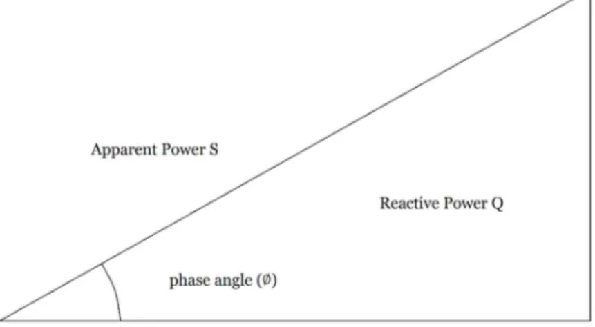
AC consists of a voltage and a current which alternates with a sinusoidal waveform [6]. The periodicity of the waveform, in European grid, is 50𝐻𝑧. A load draws appar-ent power (𝑉𝐴) which consists of a voltage and a currappar-ent, see formula (3). Apparappar-ent power can be broken down into two different components. The components are re-ferred to active power (𝑊) and reactive power (𝑉𝐴𝑟), see formula (4). AC has another important property called the phase angle (∅) which comes from the sinusoidal be-haviour. The phase angle in a circuit at a specific node is the difference between volt-age and current in time, voltvolt-age is the reference and either current leads or lags the voltage in time, see formula (1,2). This phase is angle usually described together with, ∅ , where 𝑐𝑜𝑠∅ is the power factor.
The relationship is usually described in a triangle. Apparent power, denoted 𝑆, is the hypotenuse, while active power (𝑃) is on the bottom and reactive power (𝑄) is the right side. The angle relationship is between S and P. By making modifications in an AC-circuit, by using either inductors (L) or capacitors (C) or resistors (R), the angle will change.
Figure 2.2.1.1: Power triangle for AC.
For an electrical node, these relationships can be described using the following for-mulae:
𝑃 = 𝑈 𝐼 𝑐𝑜𝑠∅ (1)
𝑄 = 𝑈 𝐼 𝑠𝑖𝑛∅ (2)
𝑆 = 𝑈 𝐼 (3)
𝑆 = 𝑃 + 𝑄 (4)
where 𝑈 is the voltage (Root Mean Square; or RMS), 𝐼 is the current (RMS)
To simplify calculations complex numbers were introduced. Where resistors (R) has only real components, inductors (L) have imaginary components which are positive and capacitors (C) have negative imaginary components [6]. The imaginary compo-nents are called reactance, 𝑋 𝑎𝑛𝑑 − 𝑋 . These reactances form an impedance which will have a phase angle in the complex plane. And if the impedance is not present in a formula its phase angle contribution is appended to the current e.g., 𝐼∠15°. This phase angle also denotes how much active power or reactive power is produced. Hav-ing a current magnitude of 1𝐴 with a phase angle of 0° would mean 0 𝑉𝐴𝑟 and 1𝑊. Having a current magnitude of 1𝐴 with a phase angle of 90° would mean 1𝑉𝐴𝑟 and 0𝑊. Both these could be said having 1𝑉𝐴. The magnitude of the current is not changed even though the phase angle changes.
𝑈 = 𝐼𝑍 = 𝐼 ∗ 𝑅 + 𝑗(𝑋 − 𝑋 ) (5)
𝑋 = 𝜔𝐿 (6)
𝑋 = (7)
𝜔 = 2𝜋𝑓 (8)
where 𝑈 is the voltage, 𝐼 is the current, 𝑍 is the impedance, 𝑋 is the inductive reac-tance, 𝑋 is the capacitive reacreac-tance, 𝜔 is the angular velocity of an alternating cur-rent and 𝑓 its respective frequency.
Thermal energy in an AC-circuit
Thermal energy is called Joule heating or Ohmic heating in electrical circuits [6]. In an AC-circuit the thermal energy is given by resistive loads. In AC-circuits a load can be calculated by using formula (9). Usually, the circuit is not purely resistive, which means that the formula (9) needs to be modified if average power is of interest. The formula then is modified into formula (10). The heating power only has a resistive component which is the real part of the impedance. This means that imaginary parts or reactive power has no joule heating. If reactive loads are being used that shouldn’t increase the thermal energy in the AC-circuits.
𝑝(𝑡) = 𝑢(𝑡)𝑖(𝑡) (9)
𝑃 = 𝑈 𝐼 𝑐𝑜𝑠∅ = 𝐼 𝑅𝑒(𝑍) = { } (10)
where 𝑝(𝑡) is the momentary active power, 𝑢(𝑡) is the momentary voltage, 𝑖(𝑡) is the
momentary current, 𝑃 is the average active effect and 𝑅𝑒{𝑍} is the real component
In an ideal situation the capacitors and inductors wouldn’t produce any thermal en-ergy. The real capacitors and inductors have a resistive component to them and in-ductive or capacitive component, known as equivalent series resistance (ESR), equivalent series inductance (ESL) and self-capacitance. This resistive component is a small part of the total impedance of the component. Capacitors and inductors will then contribute to overall thermal energy in a circuit [7].
Capacitors
Capacitors are built up by having parallel conducting surfaces facing each other and collecting positive charges on one side and negative charges on the other one [7]. Between these surfaces a dielectric is required, it can be made of many different ma-terials, including air. This means that even two wires lying next to each other is a capacitor, although with a very small capacitance. The dielectric material is what gives the capacitor its name: film capacitors, ceramic capacitors, mica capacitors, electrolytic capacitors and vacuum capacitors.
In a capacitor a charge between the two conducting areas will create an electrical field [7]. The electrical field will increase in strength if voltage potential is rising and decrease in strength when the distance between the plates increases, see formula (15). An electrical field also loses its strength if the opposing plates are orthogonal. They should be parallel for optimal strength.
𝐸 = = − (15)
where 𝐸 is the electrical field strength, 𝐹 is the force of the field, 𝑄 is the electrical charge and 𝑑 is the distance between the dielectric surfaces.
Capacitance is the ability of a capacitor to store energy and the unit is called Farad, see formula (16) [6, 7]. One farad is when one coulomb per plate with one volt being the potential over the capacitor, one plate has a positive charge and the other one has a negative charge. A capacitor is charged up over time, see formula (17). What can be seen about the capacitance is that if permittivity or area increases then the capaci-tance increases and if discapaci-tance increases then capacicapaci-tance decreases, see formula (18).
𝐶 = (16)
𝐶 = (17)
𝐶 = (18)
where is the rate of change in charge with respect to voltage, 𝜀 is the permittivity of the capacitance and 𝐴 is the dielectric surface area.
When using multiple capacitors (𝐶) in series and parallel, they are added opposite to resistors (𝑅) and inductors (𝐿).
Example: R = R + R ⟺ = + , in series.
= + ⟺ C = C + C , in parallel.
When a capacitor is empty and connected to a DC power supply then a current will be created that charges the capacitor [7]. Initially the capacitor behaves as a short circuit, due to the rush of charges into the unsaturated surface materials. Already after one time constant (denoted 𝜏, see formula (19)) the capacitor has reached 63% charge. The current will taper off after 5𝜏 when it is approximately 99% charged and behave as an open circuit. When discharging the opposite happens, 63% of the charge is lost after 1𝜏. When finding out how much energy, denoted 𝐸, that is stored in a capacitor one can use the kinetic energy formula with some modifications, see formula (22).
𝜏 = 𝐸𝑆𝑅 ∗ 𝐶 (19)
𝐼 = ∗ 𝑒 (20)
𝑄 = 𝐶𝑈 1 − 𝑒 (21)
𝐸 = = (22)
where 𝐼 is the capacitor current, 𝑡 is time of charge, 𝑄 is the capacitive charge and 𝐸 is the kinetic energy stored in the capacitor.
The capacitor current is a function of the time derivate of the voltage [7]. If the volt-age is steady, DC, there is no current flow. In the case of steady sinusoidal AC voltvolt-age across the capacitor then a simplified mathematical solution can be used with the frequency. This is the reason why capacitors ‘block’ DC and ‘pass’ AC.
𝐼 = 𝐶 ∗ (23)
𝐼 = 𝜔𝐶𝑈 = 2𝜋𝑓𝐶𝑈 (24)
where is the rate of change of the voltage.
A capacitor has an impedance because it has a capacitance, an inductance and a re-sistance since a capacitor is not an ideal component, see formula (25) [7]. This means that a capacitor has an active power but a very small one which presents as heat
losses in a capacitor, but it should be noted that this resistance also has a frequency component, as discussed in 2.2.4. ESR is usually in the range of milliohms, 𝑚𝛺. ESR will become the dominant factor with increasing frequency, this is because with in-creasing frequency the reactance will be reduced, the inductance will increase and only the ESR will remain. A capacitors resonant frequency is when inductance and capacitance is of equal magnitude.
𝑍 = (𝐸𝑆𝑅) + (𝑋 − 𝑋 ) (25)
𝑃 = 𝐼 ∗ 𝐸𝑆𝑅 (26)
The general lifetime of a capacitor is usually doubled by every reduction of 10℃ [7]. However different dielectrics have different aging processes which means that man-ufacturers will specify other lifetimes for specific capacitors.
𝐿(𝑇 ) = 𝐿(T ) ∗ 2 (27)
where 𝑇 is the variable temperature, 𝑇 is the rated temperature and 𝐿(𝑇 ), 𝐿(𝑇 ) are the expected lifetimes of a capacitor at the respective temperature levels.
Permittivity
Permittivity is an important aspect of a capacitor. Permittivity is a measure of how a dielectric is influenced by an electrical field [7]. The dielectric rearranges its positive and negative charges to align with the electrical field and a displacement electrical field can be defined with formula (12). It should be noted that this permittivity isn’t a linear function. It’s affected by a multitude of factors: frequency, humidity, tem-perature, non-linear dielectric materials and other variables.
𝜀 = 𝜀 𝜀 (11)
𝐷 = 𝜀𝐸 (12)
where 𝜀 is the total permittivity, 𝜀 is the relative permittivity, 𝜀 is the permittivity of vacuum and 𝐷 is the displacement field of the capacitor.
Relating to permittivity there is something called electric susceptibility, 𝜒 [7]. This relates to how easy a dielectric rearranges its positive and negative charges to an electrical field.
The dielectric
The dielectric is the material that gives the capacitor its properties and is expressed as permittivity [7]. The dielectric constant is the relative permittivity, 𝜀 , which is used to calculate the capacitance of a capacitor. Vacuum has the dielectric constant of one.
Dielectric breakdown strength is an important characteristic for a dielectric [7]. This is the measure of the material to withstand high voltage potential differences. It is measured in 10 𝑘𝑉 AC per mm or 50 𝑘𝑉 DC per mm. If a voltage potential difference is greater than the dielectric breakdown strength, then a current will start to flow across the conductors. This called a dielectric breakdown. When this happens, the dielectric can either be damaged or recover when the voltage potential difference is reduced. In power transmission a gas called sulfurhexaflourid (𝑆𝐹 ) is used as a lectric and it recovers as soon as the voltage potential difference is lower. Many die-lectric gases have this ability. Many diedie-lectrics don’t survive a break down such as electrolytical capacitors, film capacitors and other solids. The dielectric strength is influenced by temperature, frequency and the electrodes.
The dissipation factor is the third factor in dielectrics [7]. This factor is the ratio of equivalent series resistance (ESR) and reactance (𝑋 ). It is also the inverse of quality factor of a capacitor. ESR is more than just the dielectric resistance and is composed of insulation resistance (dielectric) and series resistance e.g., solder, wire resistance and end connections. As seen in the formula (14, 8) the dissipation factor increases with frequency. In the same formula (14) it can be seen that the loss is the ratio of real power and apparent power. Dissipation factor is called many things: tangent of loss (tan 𝛿), loss angle and power factor of capacitors.
𝐷𝑖𝑠𝑠𝑖𝑝𝑎𝑡𝑖𝑜𝑛 𝐹𝑎𝑐𝑡𝑜𝑟 = 𝐼 ∗ = = 𝜔𝐶 ∗ 𝐸𝑆𝑅 = (14)
There is also dielectric absorption. Dielectric absorption happens when a capacitor is discharged [7]. The capacitor reaches zero charge but then the dielectric reorients into original state and an increase of charge happens and a small voltage across the capacitor can be seen. This small charge will disappear over time and the voltage potential will be zero. Electrolytic and electrochemical capacitors have the biggest influence of dielectric absorption. This process can be quickened by using a short-circuit.
Different types of capacitors
Capacitors are usually divided into three main categories: electrostatic capacitors, electrolytic capacitors and electrochemical capacitors [7].
Electrostatic capacitors are non-polar. Non-polar capacitors can be placed with ei-ther lead on the positive side. The capacitors can tolerate AC because of being non-polar. There are several different ones: ceramic, mica, vacuum, plastic and- paper film or foil.
2.2.6.1 Electrostatic capacitors
Film capacitors use a plastic compound as a dielectric [7]. There are a few different dominating plastics: polyester, polypropylene, polyethylene naphtalate (PEN), poly-phenylene sulphide (PPS) and polycarbonate. Film capacitors are normally the go to capacitor for AC. Polyester type has high dielectric constant, low cost, high dielectric strength and high maximum operating temperature but varying dissipation factor with temperature, then the losses tend to be non-linear for polyester capacitors. The dissipation factor makes it hard to use the polyester type for high frequency applica-tions. Polypropylene has low dissipation factor, low dielectric absorption and good stability for higher frequencies but low dielectric constant and maximum tempera-ture is 105°𝐶. PPS has excellent properties, very low temperatempera-ture change in capaci-tance, very low change in capacitance over time and a low dissipation factor. The big shortcoming of PPS is the low dielectric constant. This makes them large compared to other capacitors with the same capacitance.
Film capacitors also come with metal infused in the dielectric and is becoming more dominant [7]. The metals that are being used is aluminium and zinc, either by them-selves or a combination. Silver can also be used in combination with the other metals. Zinc makes the capacitor more stable but is very sensitive to oxidation, which will degrade the capacitor. Metal improves the film capacitors in many ways but have disadvantages as well. One of the advantages are self-healing if there is a dielectric breakdown. When the break down happens, the metal will react and isolate the weak spot, this will give a little lower capacitance but greatly improve lifetime of the ca-pacitor. Other advantages of metallized capacitors are smaller size for equal capaci-tance. Also, if the capacitor stops working despite self-healing, the capacitor will be an open circuit while regular film capacitors will likely be a short circuit. A short circuit will likely damage other components because of thermal runaway. Disad-vantages are that the capacitors are sensitive to humidity, when being manufactured air voids can be present which decrease capacitance, very low tolerance for overvolt-age.
Mica is a good dielectric [7]. It has excellent working voltage, up to 70𝑘𝑉 and Mica-paper capacitors can exceed 150 𝑘𝑉 and withstand 100 𝑘𝐴 in surge current. Mica is very resistant to heat, chemicals and radiation. Mica has very low dissipation factor, 0.0001 to 0.0004. The dissipation factor is also very stable over time. This makes the capacitor very linear with increasing frequency. Mica has very low loss of capacitance over time and it is linear, 0.1% per year in stable environment. When being manu-factured the capacitors have very low tolerances, +/− 1%. Mica capacitors are ex-pensive and have a low dielectric constant, from 5 to 7 𝜀 , which makes them larger relative to their capacitance.
Glass is the best dielectric when it comes to performance [7]. Glass capacitors have very low dissipation factor even at high frequency, 1𝐺ℎ𝑧. They can also have lifetime up to 50 years without degradation. The capacitance is small, the capacitors are very expensive and only used when extreme precision is needed.
Ceramic capacitors are divided into three classes: ultra-stable class 1 dielectric (NPO or C0G), stable class 2 dielectric and general-purpose class 3 dielectric [7]. Class 1
dielectrics are affected little by time, temperature, frequency and voltage. They have a dielectric constant of 5 to 150 𝜀 . Class 2 dielectric and class 3 dielectric uses ferro-electric material. Because the material is ferroferro-electric the capacitance will decrease if a DC bias voltage is applied. What happens is that some of the dipoles in material get “locked” in position and the dielectric material can lose as much as 80% of its capacitance. If applying an AC bias over a ceramic capacitor it can increase the ca-pacitance [8]. The AC bias behaviour of a capacitor is usually not specified and needs to be tested. Class 2 and 3 dielectrics also differ in aging, class 2 might lose up to 5 − 10% of its capacitance, while a class 3 dielectric will lose up to 25 % over 100𝑘 hours. The capacitors also are affected by varying capacitance over temperature. Classes 2 and 3 have high dielectric constants and have good size compared to capacitance. Vacuum capacitors use vacuum as a dielectric [7]. They are large but the dielectric never degrades unless the capacitor itself is damaged. The dielectric constant is 1 which is the lowest, making them large. They can handle very high currents and high AC voltages.
2.2.6.2 Electrolytic types of capacitors
Electrolytic capacitors are polar [7]. This means that this type has a positive lead and a negative lead. The capacitors will act as a short circuit if they are fed a reversed current and will destroy the capacitor. There is something called an AC electrolytic capacitor, they behave as non-polar capacitors. AC electrolytic capacitor is two ca-pacitors that are connected with a positive lead to positive lead or vice versa. One capacitor will then act as a short circuit and the other one as a capacitor no matter how they are connected. An AC capacitor can only tolerate this for short time period, up to 3 seconds.
There are several types of electrolytic capacitors: aluminium, tantalum and niobium and are available either as liquid or solid electrolytes.
Aluminium capacitors have high capacitance compared to size even though the die-lectric constant is low, 8.5 𝜀 , but can be made very thin, only tens of microns [7]. Even though the capacitors can be made in large sizes, they have high resistive com-ponents, poor frequency characteristics, poor reliability and poor shelf life. The ca-pacitors have medium withstand voltage and are very cheap for their capacitance. Tantalum capacitors have a higher dielectric constant, 27 𝜀 [7]. Tantalum capacitors offer many benefits over aluminium type: more capacitance per unit, higher temper-ature stability, can tolerate higher reverse voltage, high reliability and good shelf life. However, the tantalum capacitors can’t withstand as high voltage, up to 125𝑉. While the aluminium ones can handle up to 500𝑉.
Niobium capacitors have the highest dielectric constant, 41 𝜀 among electrolytics [7]. Niobium has almost the same properties as tantalum but has added benefits: the material is more easily accessible, easier to manufacture, low cost and can be made smaller. The capacitors cannot be used with high voltages, usually rated under 10𝑉.
2.2.6.3 Electrochemical capacitors
Electrochemical capacitors are also known as super capacitors, ultracapacitors and are polar [7]. The reason for the name is that the capacitors are dense in energy com-pared to other types. The capacitors are dense because the dielectric can be made super thin. One of the electrodes in the capacitor is porous and allows the electrolyte to flow through it. This design increases the effective area many times. There are electrochemical double layer capacitors (ECDL) that are even more dense because they use two porous electrodes and act as two capacitors in series and increase work-ing voltage. The capacitance depends on how porous the electrodes are. The capaci-tors have low working voltages, 1.2 − 3.5 𝑉 and li-ion cap 3.8 − 4.0 𝑉, and are sensi-tive to voltage fluctuations. Because of the low voltage the capacitors are often used in series in conjunction with parallel combination. The problem is that the voltage across series capacitors can vary and management of this is required. If the voltage is allowed to increase more than ten percent, then the lifetime will be reduced by a large margin. An aluminium electrolyte with capacitance of 1𝐹 (Farad), takes 4536 𝑚𝑚 surface space and is 143 𝑚𝑚 high compared to an EDCL capacitor of 1𝐹 that takes 128 𝑚𝑚 and is 18 𝑚𝑚 high. These capacitors have similar working volt-ages, 6,3 𝑉 and 6.0𝑉 (9,10). These capacitors of course have different traits: different ESR, different frequency tolerances, different lifetime and other parameters.
Lighting measurement
Light flux is the quantity corresponding to the human perceivable light emitted from an object, defined with the unit Lumen, 𝑙𝑚 [11]. The flux of 1 Lumen projected onto a one square meter surface is defined as one Lux, 𝑙𝑥.
1 𝑙𝑥 = 1 (28)
1 Lumen is the photometric equivalent of 1 Watt. At 555𝑛𝑚 (Green-Yellow light), 1 𝑊 of effective consumed power of an LED equals 683 𝑙𝑚. The light from most LEDs occupies a light spectrum of about 20𝑛𝑚, thus having a rigid colour to most observ-ers.
LED
An LED is a solid-state diode that is capable of emitting light. LEDs consist of a sem-iconductor material doped with a lighter or heavier element on either side of a junc-tion. The imbalance of innate electrical charge on the two sides of the junction gives the diode the ability to only pass current in one direction. This is called a PN-junction and is what gives all diodes their fundamental characteristics. When a voltage is ap-plied across an LED, electrons are given enough energy to jump into an elevated en-ergy state known as the conduction band, and current flows. Moments later, the elec-tron loses energy and falls back into its lower-level state, known as the valence band, where a photon is often emitted [11]. The emittance of photons of a certain wave-length corresponds to a difference in energy between these two states. A higher for-ward voltage is needed for an LED than for a common diode. For this reason, silicon is unsuitable as a semiconductor in the LED PN-junction, while being the most
com-mon for regular diodes. The first LED semiconductor was made from Gallium Arse-nide. They have since been made with other materials including Gallium Arsenide Phosphide and Indium Gallium Nitride.
An LED can be described as a constant voltage load since it can be supplied with the same voltage and current passively throughout its lifetime. The light output of an LED is linearly dependent on the current - within a rated range, twice the current results in twice the lighting flux. The forward voltage drop of an LED determines its colour, with its peak wavelength varying up to 10% in tolerance between individual components [11]. The voltage drop for most LEDs is approximately 2𝑚𝑉 / 1°𝐶. In today’s electronics market, modern LED usually have forward voltage of 2𝑉 or higher, depending on LED base colour.
Figure 2.2.8.1: Typical LED package assembled with printed circuit [12].
White LEDs can be made from putting a phosphor dot over the emitting surface. Phosphors have a wide light spreading spectrum and can thus be used with a blue LED to create a wider wavelength profile of the light [11]. The phosphors can be dis-tributed in three different ways in the encapsulant:
- Proximate distribution, where the phosphors are spread throughout the en-tire encapsulant [13].
- Conformal proximate distribution, where the phosphors surround just the LED die.
LEDs can be classified based on their power ratings:
- Low power LEDs consume less than 1 𝑊. Micro-LEDs can be fed as little as 2 𝑚𝐴 [11]. In general, low power LEDs output more lumen per current than their more powerful counterparts.
- Medium power LEDs consume between 1 − 3 𝑊. Basic LEDs are usually fed 20 − 80 𝑚𝐴.
- High power LEDs, also called power LEDs, consume more than 3 𝑊 [12]. Power LEDs are usually fed currents in the range of 350𝑚 − 1 𝐴 and can be used in a variety of applications including signalling, traffic lights, vehicles, agriculture and performance stages.
One drawback of LEDs are their thermal characteristics. The lifetime of an LED de-creases significantly with surface and/or ambient temperature. At the same time, in the context of traffic signals, some heat can be useful or even necessary e.g., to melt snow off traffic lights.
Breakdown issues with LED
There are multiple reasons why LEDs fail. They have been categorised as: electronic failure, LED-failure, moisture ingress, material degradation, colour shift, other com-ponents, see figure (2.2.9.1) [13].
Thermal failures in LED
LEDs are sensitive to thermal stress which is a combination of current and the am-bient temperature [13]. The temperature that affects the LEDs will lead to poor per-formance. The poor performance will make heat dispersion over the whole LED package to be non-uniform which lead to degradation of the LED. This degradation does not occur when the LED is switched off. The reason for lack of degradation is because there is a diffusion process happening inside the LED which requires a flow of electrons.
High temperatures, 180 − 250 °𝐶, will degrade the LED in such a way that it will start to behave nonlinear in regard to its rectifying behaviour [13]. The rectifying behav-iour is that a diode only leads in one direction. If the potential difference, voltage, is big enough then the diode will start to conduct current and normally this has a linear behaviour. The linear behaviour is that the bigger the potential difference the more current it will lead.
In medium to high powered LED there is a problem with the encapsulant either rais-ing or curlrais-ing [13]. Raisrais-ing is when a part of the encapsulant raises from the LED-die and then the blue light from the LED-LED-die takes a longer path to the phosphor. When the path is longer to the phosphor a colour shift will occur. Curling is when the edges of the encapsulant raises and there is an escape of blue light from the LED-die. These phenomena do not really happen to the remote phosphor distributions since they are in general a cooler design than the other types of distributions.
There is a correlation between temperature and colour temperature over time [13]. When temperature is high then the colour temperature drops faster. The main rea-son for this is that there is a discoloration of the encapsulant. The discoloration is yellow and will distort the colour temperature. Colour temperature will get lower which means that the light will become more yellow over time and shift towards red [12]. In a reported test of 3000 ℎ of testing for three different temperatures and light
intensities: [80, 100, 120] °𝐶 and [825, 3300, 13200] . In these tests it can be
shown the degradation of lower light intensity for the colour temperature is 360 𝐾, from 80 to 120 𝐶°. The brightest light had a degradation of 580 𝐾, from 80 − 120 °𝐶. From this test you can also see that the biggest drop happened between 80 − 100 °𝐶. The light with least light intensity had a drop of 290 𝐾 and the brightest light had a drop of 400 𝐾 [12].
The colour degradation can also be translated into lumen which was done for the light intensity test. The graph that was derived from this shows a correlation between 70% left of the Lumen in the source correlated to age and heat, see figure (2.2.10.1).
Figure 2.2.10.1: Life-time degradation over time in different temperatures with Y-axis hours [12].
Prototype LEDs
The LEDs that were used for the prototype were of model GW QSLM31.EM-H3H8-XX58-1 (replacing the previous model name GW_QSLM31.EM-H2H4-QSLM31.EM-H3H8-XX58-1) and are provided by Osram [14]. In table 1 some properties of the component are high-lighted, with respect to critical properties for an OU:
Table 2.2.11.1: Characteristics of LED model GW QSLM31.EM-H3H8-XX58-1 by Osram [14].
Luminous flux for current 65𝑚𝐴 [𝑙𝑚] 36.8
Colour temperature for current 65𝑚𝐴 [𝐾]
2700
Operating temperature, min./max. [°𝐶] −40/+105
Electrical thermal resistance [𝐾/𝑊] 8.6
Forward voltage, min./typ./max. [𝑉] 2.60/2.72/2.95
Forward current, min./max. [𝑚𝐴] 10/400
Surge current for 𝑡 ≤ 10µ𝑠 [𝑚𝐴] 600
Power supply designs for LED applications
An LED application consisting of one or several LEDs works best with constant cur-rent and a voltage that does not exceed the rated voltage of the LEDs [11]. Increasing the temperature of the LED reduces its ESR, thus reducing the forward voltage. This implies that the current increases and generates more heat. Because of this cascading effect it is vital for any application to regulate the current flow through the LEDs. Since there is a component tolerance on the forward voltage of each LED, putting LEDs in parallel means that one of these LEDs or arrays of LEDs will draw more current than the others. Very few designs consider putting LEDs in parallel for these reasons. With several smaller LEDs it is easier to spread the light and divert heat from the circuit.
In the book “Power Supplies for LED Driving” by Winder [11], several design principles for power supplies are covered. A number of them are presented in sections 2.2.13 – 2.2.16 and are reviewed with respect to their use in this study.
Passive Control
In this very basic design for a series of LEDs, resistors are put in series with the LEDs, thus restricting the voltage across the LED line. Winder defines this as passive con-trol. The increased total resistance with the resistor plus the ESR of the individual LEDs will make more supply voltage needed to increase the current in the LEDs. There are several problems with a passive control design. It can only work if the sup-ply voltage stays identical throughout the whole lifetime of the application. If the circuit is to tolerate variations or transients in the supply voltage, the resistance needs to be increased. At the same time, if the resistance is too high it is likely the LEDs are not supplied with enough current.
Linear voltage regulator with shorted load protection
Figure 2.2.14.1: Actively controlled LED power supply circuit with linear regulator LM317 and shorted load protection [11].
With active control the current through the LEDs can be well regulated. In this de-sign, the load current is adjusted by a linear regulator. In figure 6 one such imple-mentation with a 3 terminal linear regulator LM317 from Texas Instruments is shown [11]. In the case of a short-circuit, where a higher current than normally flows to the regulator, the high input voltage can still produce stress that in the long term harms the regulator. With shorted load protection, overcurrent can pass through a Zener diode and activate a fail signal for diagnostics and main power supply regula-tion.
According to Winder it is easy to understate the power consumption of a linear reg-ulator, during operation under normal conditions or otherwise. A lot of heat is gen-erated when regulating the voltage, and this affects the ambient temperature and can cause performance and longevity issues for the LEDs.
Buck Converter
A buck converter, also known as a step-down converter, is a switching drive where switches can regulate the voltage and current to a load in a circuit. Winder proposes the use of this design for applications where the load voltage is lower than the supply voltage. If the current through the load reaches a threshold value, then the power supply switch is opened, and the ground switch is closed. This is keeping the current flowing to the load. These switches are mostly implemented using MOSFET transis-tors and/or diodes. For a synchronous buck converter both switches are actively con-trolled transistors. In the case of an asynchronous buck shown in figure (2.2.15.2). The power supply switch is swapped for a “flywheel” diode. With MOSFET switches these channels can be alternated very fast, usually between 25𝑘𝐻𝑧 − 2𝑀𝐻𝑧, depend-ing on model. If needed, pulse width can be adjusted up 85% of a duty cycle.
The line from the switches to the load, in this case a LED string is in series with an inductor. The inductor acts as a low pass filter to control the current, limiting the rate of change in the current. This is useful for the control system which has a limited sample rate for electrical measurements and needs some time to react to changes in current.
Figures 2.2.15.1: Concept for a general buck driver [11].
Boost converter
A boost converter, also known as a step-up converter, is a switching drive circuit where a sequence of capacitances is charged and then periodically pass on the charges forward from the input line to the output line. The switches are placed so that every capacitance in the chain either receives charges from the previous step or passes on charges to the next capacitor.
Winder proposes the use of this design for raising the voltage of the output relative to input. This is useful for LED applications where a small power supply drives a set of LEDs with a forward voltage that cannot be provided by just the power supply alone. In contrast to a transformer, which operates only on AC lines and cannot be used for rectified lines, the boost converter does the same task on a DC line.
Inductors can be put in series with the boost converter subcircuits to store energy between switching cycles. The energy in the inductor is released when the switch to the next capacitor step is closed, which stabilizes the current flow in the driver. Boost converters can be implemented synchronously using only transistors, or asynchro-nously replacing the forward switch with a diode. The diode needs to be adjusted for the expected charge flow for each booster step.
Figure 2.2.16.1: Theoretical inductor-based boost converter [11].
Figure 2.2.16.2: Practical implementation of an asynchronous inductor-based boost converter [11].
A problem with boost converters is that there are pronounced ripples in the output voltage with the same period as the switch cycles [11]. These ripples can put electrical stress on the LEDs and other components in the circuit. These ripples can be man-aged with closed loop feedback control of the duty cycles of the switches. Adjusting the output line capacitance so, that the rate of charge and discharge is not too fast can also help reduce the voltage ripples.
The following is a mathematical description of the energy transfer process of the booster converter in figure (2.2.16.2). It is assumed for this model that the transistor and diode are ideal, and that no voltage drop or power dissipation occurs in these components. For the switching period 𝑇 for the transistor 𝑄 , the fractions of the duty cycle where the switch is closed and open are denoted 𝛿 and 1 − 𝛿 respectively. The momentary electrical charge 𝑞 of a capacitance is described by the formula.
𝑞 = 𝐶𝑢 (29)
where 𝑢 is the momentary voltage in the capacitance [15].
𝑞 = 𝐶𝑢 , 𝑖 = ⇒ 𝑖 = 𝐶 (30)
where 𝑖 is the momentary electric current to the capacitance and , are the
rates of change of the charge and voltage.
The magnetic flux 𝛷 of an inductance is described by the formula.
𝛷 = 𝐿𝑖 (31)
where 𝐿 is the inductance and 𝑖 is the momentary current flowing through the in-ductance.
𝛷 = 𝐿𝑖 , 𝑢 = ⇒ 𝑢 = 𝐿 (32)
where 𝑢 is the momentary voltage across the inductance and is the rate of change of the current through the inductance. The cumulative energy storage of a capacitor and an inductor are related to the power consumption in these components while charging, see formulas (34-35) [11]:
𝐸 = ∫ 𝑝 𝑑𝑡 = ∫ 𝑖 𝑢 𝑑𝑡 = 𝐶 ∫ ∗ 𝑑𝑡 = ∗ 𝐶𝑉 (34)
When 𝑄 is closed, the entirety of the input voltage is dropped across the inductor 𝐿 .
𝑈 = 𝑉 (36)
𝑈 = 𝐿 ⇒ 𝛥𝐼 , = 𝛿𝑇 ∗ = (37)
where 𝑉 is the input voltage, 𝛥𝐼 , is the total change in inductor current during 𝛿𝑇.
In accordance with formula (32), until the inductance current is saturated or 𝑄 opens the current 𝑖 increases linearly. When 𝑄 is opened and stays open long enough, the total energy in 𝐿 is transferred across the diode to 𝐶 . The voltage across the inductor then corresponds to the voltage difference between the input and the switch.
𝐸 = 𝐸 ⇒ ∗ 𝐶 𝑉 = 𝐿 𝐼 ⇒ 𝑉 = 𝐼 (38)
Û − 𝑈 = 𝐿 ⇒ 𝛥𝐼 , = (1 − 𝛿)𝑇 ∗ Û (39)
where Û denotes the voltage across the open switch 𝑄 and 𝛥𝐼 , denotes the total
change in inductor current during (1 – 𝛿)𝑇.
As shown in formula (38), the voltage boost is proportional to the nominal peak cur-rent in the inductor. In a steady state, the voltage across 𝐶 is greater than the input voltage due to the charges transferred from 𝐶 , but also due to the voltage polarity of the charged inductor 𝐿 . During a steady state period 𝑇, for a continuous current in the inductor, the change in inductor current is cyclical. From this, an approximate formula for the output voltage can be derived:
𝛥𝐼 , = 𝛥𝐼 , ⇒ = (1 − 𝛿)𝑇 ∗ Û (40)
⇒ 𝑈 = Û − 𝛥𝑈 = − 𝛥𝑈 (41)
where 𝛥𝑈 denotes the range of the output voltage ripple. Given a high enough
switching frequency and a large enough output capacitor, the current charging the output capacitor can be approximated to a constant value during steady state [15],
denoted 𝐼 . Then the range of the output voltage ripple can be calculated:
In summary, there are some critical aspects that need to be considered for designing a well-functioning booster converter. The output voltage is related to the duty cycle of the switch. The output voltage ripple can be greatly reduced with a sufficiently large output capacitance. For an ideal switch, the higher the switching frequency is the smaller the inductor current ripples become. However, in practice, there needs to be a compromise in frequency with regards to transistor performance and the abil-ity for a controller to change the gate voltage. A sufficiently large inductor must be used for the continuous current flow. However, if the inductor is too large, the booster becomes slow when reacting to changes in the input voltage.
3 Methods and results
Here are methods that were used in this study and the results are also presented. Method summary
The sections of the prototype that were considered for study, were the reactive com-pensation and rectification, the DC power supply subcircuit and the LEDs. The ther-mal and electrical properties of capacitances were studied, with the aim of finding equipment that could withstand some of the stresses that come with the reactive compensation.
Electrical analysis by means of simulation was possible with the use of a set of soft-ware. OrCAD was used for designing the prototype schematics, where the sections of the prototype were designed individually. PSpice was used to simulate the OrCAD schematics and present the results for analysis. Data from these simulations was ex-ported to MATLAB for further processing and formatting for presentation.
The schematics for the different sections were studied and designed through iterative process. The first versions of the schematics were designed as a proof of concept, with no design or component optimisation. When these sections had been simulated, the data was analysed for further improvements.
Basic circuit analysis
The model of the 48𝑉𝐴𝐶 prototype had an input current for day-mode, night-mode and continuity test. These values are presented in table (3.1.1.1).
Table 3.1.1.1: *The continuity test was specified in ohms in Alstom’s confidential doc-ument but for this thesis it was converted into a current [5].
Operation mode Current [𝑚𝐴] Deviation [%]
Day current 40 +/− 10
Night current 25 +/−10
Continuity test 38 +/−5*
Early in the thesis work this current together with voltage was used to determine the loads, using formula (1).
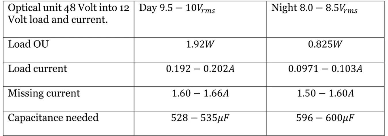
It was needed to find out Trafikverket’s recommended current and voltage for the shunting signal lamps, for 24𝑊 and 12𝑉𝐴𝐶, see table (3.1.1.2).
Table 3.1.1.2: Trafikverket’s requirements for white shunting lamps [2].
Operation Voltage [𝑉] Current [𝐴]
Day-mode Max 10,0 Min 9,5 Max 1,85 Min 1,80 Night-mode Max 8,5 Min 8,0 Max 1,70 Min 1,60
The current that was needed to be added for the unit to be accepted by the interlock-ing system, was extrapolated by usinterlock-ing formula (5, 43).
𝐼 = 𝐼 + 𝐼 + ⋯ + 𝐼 (43)
where total current is denoted 𝐼 for 𝑛 number of currents.
The amount of reactance needed was determined by using the missing current by using formula (5). Then the needed capacitance was extrapolated from using formu-las (6, 7).
Choosing components for reactive power
A literature study about reactive power and capacitors was performed. According to two studies it was beneficial to use reactive power to compensate for thermal stresses in components and the best results was obtained by using reactive power that is rep-resented by capacitors [16, 17]. Therefore, the focus became to study capacitors more closely. While studying capacitors, it was mentioned that capacitors are used to lower thermal impact in circuit design [7]. There was also the physical limitation of the OU, the unit is quite small 7040𝑚𝑚 [5]. It was apparent from the basic circuit analysis that quite big capacitance was needed. There was also a need for the capacitors to be on the AC side because of reactive compensation, since in DC the reactive compen-sation would not have worked [18].
An issue when choosing the capacitors was the temperature deviation and ageing of the capacitors. Many capacitors capacitance vary with age and temperature and sometimes these factors interact [7]. Also, ESR is affected by temperature and fre-quency which impacted choices [7,11]. These factors impacted because of the wishes of Alstom for their product, Alstom wants the capacitors to last 10 years.
Calculations of the board space, ageing and active power the capacitors would con-tribute to the circuit, formulas that was used (5, 10, 27, 44-46) [19].
𝐴𝐹 = 1 + (𝐴𝑅)(log(𝑅𝐻) − log(𝑇𝐻)) (44)
𝐴 = 𝑙𝑤 (45)
𝑉 = 𝐴ℎ (46)
where 𝐴𝐹 is the ageing factor of a capacitance, 𝐴𝑅 is the aging rate, 𝑅𝐻 is the number of reference hours and 𝑇𝐻 is the number of tested hours. The volume 𝑉 is calculated using length 𝑙, width 𝑤 and height ℎ.
Reactive compensation and rectification
An electrical analysis was done for an implementation of the reactive compensation and rectifier section of the prototype. A proof-of-concept schematic was initially cre-ated in OrCAD, with the intent of imitating the rectifier of the previous 48𝑉 proto-type. A capacitive compensation was placed on the AC side of the circuit, where it could draw a reactive power. A generic load of 1𝑘Ω was used to emulate the current consumption of the rest of the circuit. A large electrolytic capacitor was placed on the DC side. The capacitor value was picked arbitrarily for a sufficient analysis of the rectified voltage. The electrical circuit was simulated in PSpice and is presented in figure (3.1.3.1).
Figure 3.1.3.1: First iteration of the reactive compensation and rectification subcir-cuit.
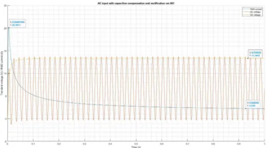
Figure 3.1.3.2: AC voltage and current through the voltage source and rectified DC voltage of the proof-of-concept subcircuit.
The data from figure (3.1.3.2) indicates that the reactive compensation can, given the correct parameters, draw a sufficient current for the interlocking system to detect if the circuit is operational. The instant the voltage is stepped up, there is a transient current of approximately 20 𝐴. The capacitances have to be adapted for these kinds of currents.
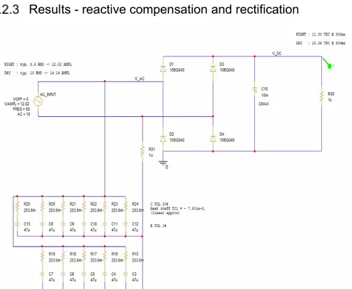
A more detailed model was developed after the initial model. The reactive compen-sation was more correctly modelled, where several smaller capacitances of the type multilayer ceramic capacitor (MLCC). The capacitances were modelled with an ESR, represented by resistors in the schematic. A tolerance of 1% of the resistance and capacitance values was assumed. The change in capacitance with regards to operat-ing temperature was modelled with a linear coefficient 7.80 ∗ 10 .
While not an exact replication of the thermal characteristics, the peak-to-peak ca-pacitances for permitted operating temperatures were preserved. The circuit was simulated for the two operational modes for day and night, with data for tempera-tures [−40, 25, 70] °𝐶. The choice of temperatempera-tures was motivated by operating tem-peratures for the previous OU. To study the behaviour of the circuit under tolerance conditions, 50 different simulations were made simultaneously with a gaussian ran-dom distribution assigned to the values of the resistors and capacitances, defined by the 1% tolerance restriction (a.k.a. Monte Carlo simulation). The schematic for the second iteration is shown in figure (3.1.3.3). The average voltage and current (RMS) for night- and day-mode for the different operating temperatures is presented in sec-tion 3.2.3. (Note in figures 3.1.3.3 and 3.2.3.1 that the polar capacitance 𝐶 has been placed incorrectly; this was a mistake by the authors but had no implications for the simulations.)
Figure 3.1.3.3: The second iteration of the compensation/rectifier circuit.
For the final version of the schematic, some further details were added to the com-ponent models. A new ESR for the capacitance given the AC frequency of 50𝐻𝑧 was set. The datasheet for MLCC from Kemet [20] shows that the ESR is 253.60mΩ at 100𝐻𝑧 AC frequency and 25°𝐶 and the ESR was assumed to be close to that value. The night- and day-mode operation AC voltage was adjusted to Trafikverkets recom-mendations of 8.50𝑉 and 1.85𝐴 for night-mode and 10𝑉 and 1.70𝐴 for day-mode, see table (3.1.1.2). The resistive load of the rest of the circuit was assumed to be 1𝑘Ω. The final iteration was simulated with a Monte Carlo simulation of 10 samples, with the average voltage and current across the capacitance bank for the operational modes and temperatures [−40, 25, 70] °𝐶 is shown in results, see section 3.2.3.
DC power supply
The goal was to provide the LED array in the prototype schematic with a 48 𝑉 DC. In this way, some parts of the schematic from the previous OU design would be possible to keep for the new prototype, including LED current regulation. With the reduced rectified voltage in mind, means of increasing the DC voltage were necessary. As pro-posed by Winder [11], a booster converter could increase the voltage supplied to the LEDs. For this power supply, Winder’s design for an inductor-based boost converter was examined and verified.
Figure 3.1.4.1: The first iteration of the OrCAD booster converter circuit, with rudi-mentary parameters settings for all components. The LEDs are replaced with a pas-sive resistive load.
Initially, an electrical analysis was done of the inductor-based boost converter design with two asynchronous steps. Switching frequencies and switching duty cycles were studied. A voltage and a current that would mimic the 48𝑉𝐴𝐶 OU specifications and these were set as the bounding factors for these iterations. The circuit schematic was realised with models provided from the standard component library in Or-CAD/PSpice, with some ideal components not possible to use in a real-life applica-tion. These ideal components were assumed to be non-essential for the design and could therefore be replaced with actual components with similar electrical proper-ties. A DC voltage supply was assumed in the model, which was to represent the Schottky diode rectified AC input voltage. In the first iteration of the model shown in figure 9, the components were picked to suffice for a proof of concept. The MOSFETs 𝑀 and 𝑀 were switched on and off simultaneously with a 50% duty cycle at 6.67 𝑀𝐻𝑧.
For the second iteration of the power supply, the second booster step was deemed unnecessary and was removed. The transistor switching frequency was decreased to 200𝑘𝐻𝑧 for a more realistic switching. It was shown that the inductor was sufficient for energy storage during the charging phase of the cycle, and an input capacitance was not needed. The second iteration became the final power supply, as some trivial tests provided evidence for a sufficient output voltage for both night-mode and day-mode. To adjust the switching duty cycle and the output capacitance correctly for the
prototype, the characteristics of the output voltage were examined using variable duty-cycles and output capacitances in PSpice.
LED-array
The LED array was briefly studied in the context of the proposed modifications to the OU. Upon examining e.g., the voltage ripples from the booster converters, a con-clusion could be made on the suitability of the LEDs. Also, a literature study was done about common failure points in LED regarding light intensity and colour deg-radation.
Results
In this section the results of the literature study and mathematical simulations are presented. The results have the same order as the method section. Graphs are in the Appendix A-C.
Results - basic circuit analysis
The simulated result for the circuit analysis is presented in the following table. Table 3.2.1.1: Describing results from basic circuit analysis.
Optical unit 48 Volt into 12 Volt load and current.
Day 9.5 − 10𝑉 Night 8.0 − 8.5𝑉
Load OU 1.92𝑊 0.825𝑊
Load current 0.192 − 0.202𝐴 0.0971 − 0.103𝐴
Missing current 1.60 − 1.66𝐴 1.50 − 1.60𝐴
Capacitance needed 528 − 535𝜇𝐹 596 − 600𝜇𝐹
Results - reactive components
In the literature study it was found that polar capacitors were not an option for the pre-study. Polar capacitors can’t support AC-voltage without being damaged [7,11,18,21]. This excluded all capacitors that have high capacitance with small vol-ume, the polar capacitors have small dielectric thickness [7]. The OU’s board space was limited, which made two types of capacitors relevant for further study [5]. The capacitors considered were ceramic multilayer capacitors (MLCC) and metallic film capacitors (MFC). MFC are traditionally used in AC-circuits but are larger than MLCC [20,22]. Only 10𝑉𝐴𝐶 was needed in the circuit and lowest rated MFC that could be found was 40𝑉𝐴𝐶 [2]. This meant that the MFC was larger than necessary because of the dielectric thickness. Considering lifetimes, both MFC and MLCC have lifetimes over 100.000 ℎ𝑜𝑢𝑟𝑠 [7]. Alstom wanted as low active power as possible be-cause that would lower the temperature inside the signal housing, which meant that smaller capacitors in parallel would decrease active power loss [7,18].
A table over space needed for the capacitors are presented below with 47𝜇𝐹 per ca-pacitor and 11 caca-pacitors was modelled with a spacing of 1𝑚𝑚.
Table 3.2.2.1: Areas of respective components and how much space on the board that is occupied. Volume of the components. *Numbers are taken from datasheets from Alstom and Kemet [5,20,22].
Alstom board
space*
MLCC* MFC*
Total area and area of compo-nents 7040𝑚𝑚 462𝑚𝑚 4529𝑚𝑚 Percentage of space occupied on the board 100% 6.56% 64.3% Volume of the capacitors 2310𝑚𝑚 69750𝑚𝑚
Graphs from modelling capacitance and active power change over temperature of −55°𝐶 and 125°𝐶, were made. Also, graphs for current through the reactive part and apparent power for the whole circuit based on basic circuit analysis, were made. The datapoints were taken from Kemet for a MLCC [20] and are of frequency of 102 𝐻𝑧 + /−0.2𝐻𝑧. The graphs can be found in appendix A.
Results - reactive compensation and rectification
Figure 3.2.3.1: Final implementation of the rectifier and reactive compensation cir-cuit.
For the final implementation of the subcircuit, a set of 11 MLCCs by Kemet are used as a capacitor bank. Voltage and current levels for the capacitance bank are pre-sented in figures (B2-B7) in the appendix. The rectification bestowed a DC voltage of 11.30𝑉 for night-mode and 13.34𝑉 for day-mode.
Results - DC power supply
Figure 3.2.4.1: Final iteration of the OU booster converter.
For day-mode the pulse width for an output voltage of 43.9𝑉 was 3.5µ𝑠, for a duty cycle of 70%. For night-mode, the pulse width of the transistor switch for an output voltage of 31.9𝑉 can be set to 3.2µ𝑠, for a duty cycle of 64%. These values for duty-cycles were chosen as duty-duty-cycles for the prototype. See tables (3.2.4.1-3) for details. Table 3.2.4.1: Day-mode voltage data for variable pulse widths and set output capac-itance of 100𝑛𝐹.
Pulse width [µ𝑠] Transient voltage peak
[𝑉]
Average steady-state volt-age [𝑉] 0.50 15.68 14.31 1.00 19.10 16.15 1.50 23.48 18.54 2.00 29.25 21.71 2.50 36.93 26.16 3.00 48.04 32.84 3.50 65.09 43.90 4.00 93.89 65.24 4.50 144.75 118.22
Table 3.2.4.2: Night-mode voltage data for variable pulse widths and set output ca-pacitance of 100𝑛𝐹.
Pulse width [µ𝑠] Transient voltage peak
[𝑉]
Average steady-state volt-age [𝑉] 0.50 13.19 12.04 1.00 16.06 13.59 1.50 19.82 15.61 2.00 24.63 18.30 2.50 31.15 22.07 3.00 40.59 27.72 3.50 55.03 37.09 4.00 79.49 55.19 4.50 122.95 100.32
Table 3.2.4.3: Range of steady-state peak-to-peak voltages for variable output capac-itances and set pulse width 3.5µ𝑠 (day-mode), 3.2µ𝑠 (night-mode).
Output capacitance [𝑛𝐹] Peak-to-peak steady state
voltage, day-mode [𝑉]
Peak-to-peak steady state voltage, night-mode [𝑉] 10 12.92 8.26 20 6.51 4.28 30 4.37 2.85 40 3.28 2.14 50 2.65 1.71 60 2.19 1.44 70 1.93 1.23 80 1.70 1.09 90 1.56 0.99 100 1.43 0.90
Results - LED array
The LEDs provided by the previous OU prototype (see section 2.2.11) were deter-mined to be satisfactory for the new prototype. The microcontroller was assumed functional with little modification to software. The LED current regulation of the OU was preserved from the previous prototype. The voltage ripples from the booster con-verter were not deemed problematic enough to justify changing the LEDs.
![Figure 2.2.10.1: Life-time degradation over time in different temperatures with Y- Y-axis hours [12]](https://thumb-eu.123doks.com/thumbv2/5dokorg/4617034.119073/30.892.122.697.219.641/figure-life-time-degradation-time-different-temperatures-hours.webp)
![Table 2.2.11.1: Characteristics of LED model GW QSLM31.EM-H3H8-XX58-1 by Osram [14]](https://thumb-eu.123doks.com/thumbv2/5dokorg/4617034.119073/31.892.155.815.326.751/table-characteristics-led-model-gw-qslm-em-osram.webp)
![Figure 2.2.14.1: Actively controlled LED power supply circuit with linear regulator LM317 and shorted load protection [11]](https://thumb-eu.123doks.com/thumbv2/5dokorg/4617034.119073/32.892.246.549.413.698/figure-actively-controlled-supply-circuit-regulator-shorted-protection.webp)
![Figure 2.2.16.2: Practical implementation of an asynchronous inductor-based boost converter [11]](https://thumb-eu.123doks.com/thumbv2/5dokorg/4617034.119073/34.892.189.581.818.1051/figure-practical-implementation-asynchronous-inductor-based-boost-converter.webp)
![Table 3.1.1.1: *The continuity test was specified in ohms in Alstom’s confidential doc- doc-ument but for this thesis it was converted into a current [5]](https://thumb-eu.123doks.com/thumbv2/5dokorg/4617034.119073/39.892.153.816.748.921/table-continuity-specified-alstom-confidential-thesis-converted-current.webp)