FACULTY OF ENGINEERING AND SUSTAINABLE DEVELOPMENT
.
Single-Layer Metamaterial Absorber for Radar
Application
Motasim Ahmed Mohamed Ali
Sep 2016
Master’s Thesis in Electronics/Telecommunication
Preface
This thesis is a complementary project for the master’s degree in electronics with specialization in telecommunication, from University of Gävle, located in Sweden. Several persons have contributed in this thesis practically, academically and supportively.
I would like to take this chance to thank my supervisors Daniel Rönnow from the University of Gävle, Daniel Andersson and Patrik Ottoson from Radarbolaget for the valuable input, support and guidance through the thesis period. I would like also to thank Pu Sun my classmate for the knowledge we exchanged.
Furthermore, I would like to thank the Swedish Institute (SI) for the financial support for the whole period of the master’s program, and the academic staff of the Master’s program of Electronics/ Telecommunications at the University of Gävle.
Finally, I would like to thank my family for being helpful and supportive during my studies and my friends in Sweden and back home in Sudan.
Abstract
In the radar systems, the crosstalk or antenna-to-antenna interference between the radar antennas is useful in some cases. However in some application the received signal is too weak such as wall crack detection and it might affect the accuracy of the radar system. The aim of this thesis is to design, fabricate and test a single layer metamaterial absorber operates from 1 GHz to 4 GHz. The metamaterial absorber can be used as a barrier between the antennas or even in the antenna housing in order to reduce or prevent the antenna-to-antenna interference.
The method used to fulfill the goal is to shift the frequency response of a known structure by changing the dimension to the wanted band. The software HFSS used to design and simulate the proposed structure which made of L-shaped copper placed diagonally over a substrate separating it from a continuous copper plane. The simulation results exhibit a wideband absorption response of 2.42 GHz ranging from 1.9 GHz to 4.32 GHz. The structure has been simulated over the dimension variation to investigate the flexibility and sensitivity of the designed single layer structure.
The fabricated metamaterial absorber measured over the direct incident waves. The structure reveals a wideband absorption response of 1.69 GHz ranging from 2.23 GHz up to 3.92 GHz with more than 90% absorptivity. The structure also exposed that the response of the structure starts to create two bands within the wanted band by increasing the angle of the incident waves. 10° polarization angle gives more than 80% absorptivity response.
Table of contents
Preface ... iii
Abstract ... v
Table of contents ... vii
List of figures ... ix List of abbreviation ... x 1 Introduction ... 1 1.1 Background ... 1 1.2 Problem statement ... 2 1.3 Aim ... 2 1.4 Thesis outline ... 3 2 Theory ... 4 2.1 Metamaterials ... 4
2.2 Metamaterials absorber MMA ... 5
2.2.1 Absorption equation ... 6
2.2.2 Matching impedance ... 7
2.2.3 Thickness variation ... 8
3 Method and proposed single layer MMA ... 9
3.1 Method ... 9
3.2 Proposed single layer MMA ... 10
4 Simulation ... 12
4.1 Simulation setup ... 12
4.2 Results ... 12
4.2.1 Physical dimensions variation ... 15
4.2.2 Incident wave variation ... 17
5.3 Absorptivity Response ... 20
5.4 Variation of the Polarization Angle (Ø) ... 22
5.5 Variation of the Incident Angle (θ) ... 23
6 Conclusion and future work ... 26
6.1 Summary of results ... 26
6.2 Future work ... 26
List of figures
Fig. 1. Negative versus Positive refraction index [22]. ... 4 Fig. 2. Landy et al, metamaterial perfect absorber [1] ... 5 Fig. 3. Front view of the unit cell proposed broadband absorber with the incident waves direction. ... 11 Fig. 4. Reflectivity of the simulated proposed single layer MMA. ... 13 Fig. 5. Absorptivity (%) of the simulated proposed single layer MMA. ... 13 Fig. 6. Surface current distribution at the top and bottom of the proposed single layer MMA (a) f=2.3 GHz and (b) f=4.1 GHz ... 14 Fig. 7. Surface current distribution at the top and bottom of the proposed single layer MMA for 2.4 GHz ... 14 Fig. 8. Absorption response with respect to variation of patch length (l) of the proposed MMA. ... 15 Fig. 9.Absorption response with respect to variation of patch width (ω) of the proposed MMA. ... 16 Fig. 10. Absorption response with respect to variation of substrate thickness (t) of the proposed MMA. ... 16 Fig. 11. Absorption response with respect to variation of incident angle theta (𝜃) of the proposed MMA. ... 17 Fig. 12. Absorption response with respect to variation of polarization angle phi (Ø) of the proposed MMA. ... 18 Fig. 13(a) Top view of the fabricated proposed single layer L-shaped MMA (b)enlarge view. ... 19 Fig. 14. Experimental arrangement within the anechoic chamber. ... 20 Fig. 15. Comparison between measured and simulated absorptivity responses of the proposed single layer MMA. ... 22 Fig. 16. Measured Absorption response with respect to variation of polarization angle (Ø) compared with its simulated response (a) Ø = 10° (b) Ø = 20° (c) Ø = 30° and (d) comparison for all measured Ø. ... 23 Fig. 17. Measured Absorption response with respect to variating of incident angle (θ) compared with the simulated response of (a) θ =15° (b) θ= 30˚ (c) θ= 45° and (d) comparison for all measured θ ... 25
List of abbreviation
MMA Metamaterial absorber
NIR Infrared
UWB Ultra-wide band
PRBS Pseudo-random binary sequence
TX Transmitter
RX Receiver
SRR Magnetic split ring resonators ERR Electric ring resonator TM Transverse magnetic field TE Transverse electric field
HFSS High frequency electromagnetic field simulation CST Computer simulation technology
FSS Frequency selective surface PCB Printed circuit board
SEK Swedish krona
R Reflection
A Absorption
𝜺𝟎 Permittivity of free space 𝝁𝟎 Permeability of free space
𝜺𝒓 Relative permittivity
𝝁𝒓 Relative permeability
1 Introduction
In this section, background, introduction and the problem of statement will be discussed. Moreover, the section also contains the aim and the outline of this thesis.
1.1 Background
In the recent year’s metamaterial absorber MMA has become one of the most potential fields for researchers since Landy demonstrated the perfect MMA in 2008 [1]. Metamaterials are artificial designed materials providing unique properties that not found it nature [2]. Perfect lensing, invisibility cloaking, negative index of refraction, negative permeability and negative permittivity properties can be obtained using an accurate dimension metamaterials design [2]. Metamaterials can provide high absorption and small size characteristics which make it a good candidate for a microwave absorber [2]. Metamaterials can gain their properties from structure rather than composite. Therefore, changing the dimensions of the structure can lead to change in the properties of the MMA. But obtaining the wanted properties on the wanted band is the challenge. Because there are many dimensions to change on any structure and each change in one dimension gives a different response.
MMA have attracted more consideration due to their absorbing properties and simple fabrication. MMA’s are formed from random or periodic highly conductive materials like gold or copper or silver and dielectric substrates [3]. The component of the MMA can be composed into various types of split ring or periodic wires arrays fill space in one, two or three dimension [12]. In early 1990 s, Salisbury screen radar absorber was formed from a continuous resistive film placed a quarter wavelength from a metal grounded plate. The design was acceptable for some microwave applications, but the bandwidth was limited [3,4,5]. In 2008, the first MMA has been designed and simulated by Landy using two metallic layers separated by a dielectric layer [1]. The response of Landy’s MMA was on the microwave regime, but it was only for a single frequency which is at 11.5 GHz with 88% absorptivity [1].
Since the inspiration by Landy, MMA with high absorptivity in other frequency such as THz regime [6], NIR frequencies [7], and in visible realm [8] has been experimentally realized. Obtaining a wideband response was the challenge in the beginning, but researcher found many techniques to solve the bandwidth limitation.
1.2 Problem statement
In order to increase the accuracy of the radar system to cater of the various application needs, Radarbolaget AB is developing a new radar system for small signal detection. Radarbolaget AB is a radar company providing radar solutions for many applications like construction and infrastructure, steel and metal industry, energy and paper and process industry.
A digital Ultra-wide band (UWB) radar system has been developed by Radarbolaget AB. The radar system consists of a pair of antennas (TX & RX) separated by 20 cm and they are ON all the time. Where a pseudo-random binary sequence (PRBS or M-sequence) is continuously transmitting and receiving the reflected signal for processing the data.
Most of the applications claim a small signal detection such as wall crack or detection in the dusty and humid environment. Since the applications demand sensitivity, the crosstalk is a big factor regarding accuracy. The crosstalk is the antenna-to-antenna interference and it’s useful in order to get a good reference point in the signal. But, when the crosstalk is considerable, it might create a dynamic problem like looking to birds in front of the sun. In general, the crosstalk is affecting the radar when it is used for small signals detection.
There is more than one way to reduce the crosstalk, such as separating the radar antenna, placing a metal plate between the antennas or shielding the antennas housing with a UWB absorber in order to decrease the reflection inside the housing of the antennas and then reducing the crosstalk. In our case, separating the antennas is not reliable due to the installation regulations. And placing a metal plate between the antennas is not practically effective. So, shielding the antenna housing with an UWB absorber has been chosen in order to reduce the reflection inside the antenna housing, therefore reducing the crosstalk.
1.3 Aim
As discussed in the problem statement, the crosstalk is affecting the system. So the aim of this thesis is to reduce the crosstalk between the antennas as much as possible and that can be obtained by shielding the antenna housing with a single layer metamaterial absorber. Shielding the antenna housing with the single layer MMA would reduce the reflection inside the housing; therefore the interference between the two antennas reduces. The single layer MMA shall be designed, construct and test over its absorptivity of the electromagnetic waves on the frequencies from 1 GHz to 4 GHz. Reducing the
antenna-to-antenna interference can improve the accuracy of the system and the distance between the antennas can be reduce which will develop the system.
1.4 Thesis outline
Section 2, describes the theory of the MMA, the method followed for the design and the design of the proposed single layer structure. In section 3, the simulation process and results will be discussed and section 4, demonstrates fabricating and testing of the proposed single layer structure and measurements steps. Lastly, section 5 will conclude the whole thesis and the further work to be done.
2 Theory
In this section an interpretation of metamaterials and its properties has been discussed. Metamaterials absorber MMA and its applications and absorption mechanism taking Landy structure as an example has been also discussed. The section includes also, matching impedance between the structure and the free space in order to reduce the reflection from the interface. Moreover, the section explained the absorption equation and its simplification. Lastly, the section covers the thickness variation of the materials and of the entire structure and how that can affect the response.
2.1 Metamaterials
Metamaterials are artificial materials that cannot found in the real life. It can provide exotic electromagnetic effects that impossible to achieve with natural materials. It consists of arrays of structured subwavelength elements. Remarkable properties that can breakthrough some limitations can be obtained with an accurate dimension design [2]. Metamaterials can gain their properties from its structure rather than composite. Negative index of refraction η= √𝜀ᵣ 𝜇ᵣ, where 𝜇ᵣ(ω) and 𝜀ᵣ(ω) are magnetic permeability and electric permittivity respectively, is one of the powerful metamaterials properties [9]. Fig. 1 illustrates the negative versus positive refraction index effect on incident light ray.
Fig. 1. Negative versus Positive refraction index [22].
[10] Has proved that metamaterials are a marvelous candidate for antennas, radar imaging, selective spectral detection, cloaking and as demonstrating in this report absorbers and many more applications. Metamaterials are designed into various types of split rings or periodic arrayed formed from highly
2.2 Metamaterials absorber MMA
As mentioned in the introduction section, the first MMA was designed by Landy in 2008. The structure consists of three layers, two metallic layers separated by a dielectric. The top layer made of copper and formed in an electric ring resonator (ERR) that can supply the electric response along with the ground plane at a specific frequency by coupling the incident electric field. The ground plane metallic layer, consists of a copper cut wire which is separated from the top ERR by FR4 dielectric substrate layer. The antiparallel currents in the center of the ERR and the cut wire produces the magnetic coupling [1]. The frequency response of the structure related to the dimensions of the ERR and the thickness of the dielectric and it can be tuned. Fig. 2 demonstrates the perfect MMA designed by Landy and the incident wave’s direction and the structure response. Where, the blue, green, and red signals representing transmission, reflection and absorption signals respectively. In order to plot the absorption of the structure, a special equation has been used as we will see and discuss in this theory section.
Fig. 2. Landy et al, metamaterial perfect absorber [1]
The tuning can be obtained by changing the dimension or geometry of the ERR. The electric response of the structure can be changed by tuning dimensions and size of the structure while changing the thickness of the dielectric can change the magnetic response. All the efforts have been done so far resulted with, the major loss in microwave regime for most of the structure is through the dielectric [1,13]. Since the structure is related to the wavelength, adjustment of the size permits tuning to the frequency [14].
Later, MMA structures have been simplified by using a continuous ground plane instead of the cut wire used before. The continuous ground plane prevents the transmission, while the ground plane and the ERR providing the impedance matching for zero reflection [14].
2.2.1 Absorption equation
Normally, the reflectivity of any surface can be calculated using Fresnel or many kinds of instruments. But measuring the absorptivity of a surface needs special equations, because both transmission and reflection are involving. The absorption equation needed in both cases; simulation and measurements because many software don’t calculate the absorption response. Therefore, the absorption equation needs to be entered manually.
In order to characterize the absorption of any absorber, scattering parameters of reflection and scattering parameters of transmission should be considered. Equation (4) used to calculate the absorption of the absorber and it has been derived from Fresnel equations [25],
|𝐴(𝜔)| = 1 − |𝑆11|2− |𝑆21|2 (4)
where
𝐴 = Absorption.
𝑆11 = scattering parameter of reflection. 𝑆21 = scattering parameter of transmission.
For the simplified structure, the continuous ground plane blocks the electromagnetic waves and prevents any transmission through the structure [25],
|𝑆21| → 0 (5)
So the absorption equation changes to
|𝐴(𝜔)| = 1 − |𝑆11|2 (6)
The simplified absorption equation (6) has been used in the following simulation and experimental sections.
The face of the structure or the surface impedance of the composite structure should be designed in a way to be matched to the free space impedance to obtain zero reflection on the surface interface [15].
Moreover, the interface material should have the specific impedance conditions to make the reflection as less as it can be.
2.2.2 Matching impedance
The surface impedance of the structure 𝑍(𝜔) can match the intrinsic impedance of the free space 𝑍₀. The match in impedance between the surface of the structure and the free space leads to minimizing the reflection of the incident waves from the interface of the structure. It means, it will prevent or reduces the reflectivity of the interface and the absorptivity process will apply in all or most of the incidence waves within the structure band. The free space impedance is related to the permeability of the free space μ₀= 4𝜋×10−7 H𝑚−1 and the permittivity of free space and ε₀=107/4𝜋𝑐2F𝑚−1
[24]. 𝑍₀= √𝜇₀/ 𝜀₀ = √4𝜋 × 10−7/ 107 4𝜋𝑐2 = 377 ohm (1)
The surface impedance of the structure 𝑍(𝜔) is calculated using the magnetic permeability μ(ω) = μ₀ μr(ω) and electric permittivity ε(ω) = ε₀ εr(ω), where μr(ω) and εr(ω) are the related permeability and the related permittivity respectively as follow[25],
𝑍(𝜔) = Z₀√𝜇(𝜔) 𝜀(𝜔)= Z₀
(2)
Where μ(ω) = 𝜀(𝜔)
Therefore, reflectivity of the surface impedance can be minimized when [25],
|𝑆11(𝑤)| = |𝑍(𝜔) − Z₀ 𝑍(𝜔) + Z₀| → 0
(3)
One of the magical properties of the metamaterials is that it gains their properties from the structure rather than the composition as mentioned before. So just by changing the dimensions, size, thickness or the shape of the structure, the relative permeability and the relative permittivity of the structure can be changed, therefore the properties [23]. The major loss in microwave regime for most of the structure is through the dielectric thickness [1,13]. Therefore the dielectric thickness variation of the
2.2.3 Thickness variation
The absorptivity can be affected by many factors, such as substrate thickness, material thickness, the angle of incident waves and polarity of incident waves. There is a strong relation between the absorption and the thickness. In [12], they proved that for a perfectly impedance matched medium to free space, increasing the thickness of the magneto-dielectric medium leads to increasing in absorptivity. And by further increasing of thickness, absorptivity saturates and begins to gain bandwidth, which is useful in order to design an UWB absorber.
[16] Studied absorptivity on one structure by changing the dielectric thickness. They found that, by increasing the substrate thickness and fixed the other dimensions, absorptivity can be obtained in the near same frequency response. The slight shift in the frequency response is due to the mismatch between the structure and the free space impedance. They have also discovered that, by increasing the thickness to a certain value, the ERR resonators currents are no longer influenced by the currents producing from the ground plane. That is because of the big space between the two metal elements prevents the effect of the ground plane currents to contribute along with the ERR currents.
There will be small ground plane currents and in some frequencies the ground currents can be high, but the electromagnetic will be mostly absorbed by the resonators [16]. In this case, the ground plane is mainly used to block the transmission.
3 Method and proposed single layer MMA
In this section, the method used and followed to design the proposed single layer MMA and the relation between the structure size and its frequency response has been discussed. The section also includes the proposed single layer MMA and its size and dimensions.
3.1 Method
The aim of this master thesis is to design a single layer MMA structure to absorb the electromagnetic waves in the range of 1 GHz to 4 GHz. The method used to obtain the goal is to shift the response of the structure in [17] which has a bandwidth response of 2.6 GHz ranging from 4.7 GHz to 7.2 GHz covering the complete C-band. The reference structure consists of two copper layers with 0.035 mm thick separated by a dielectric layer. The top copper layer composed of two L-shaped patches placed diagonally from each other with copper conductivity of 5.8× 10⁻⁷𝑆/𝑚. The backside copper layer of
the reference structure is completely copper plan separated from the top layer with a single layer dielectric. The dielectric material is FR-4 substrate with 3.2 mm thickness and εr = 4.05 and tanδ = 0.02.
The top layer of the reference structure made up of two L-shaped patches with dimensions; patch length is 6.7 mm, patch width is 2.5 mm and the distance between the patches and the edge of the structure is 0.25 mm. The size of the entire structure is 10 mm ×10 mm with 3.27 mm complete structure thickness.
The shifting method used based on prove (1) which prove that, by increasing the dimensions and size of the structure by 100% the frequency response 𝑓0 of the structure can be shifted by half frequency
response (𝑓0/2) Prove (1) 𝑓0= 𝑐 𝜆0 𝑑 𝜆₀= constant
2𝑑 𝜆₁ = constant By replacing d, by 2d, 𝑑 𝜆₀= 2𝑑 𝜆₁ 𝜆1= 2 𝜆0 Then, 𝑓1= 𝑐 2𝜆0= 𝑓₀ 2
where 𝑓₀= the frequency response of the original dimension
𝑓₁= the frequency response of the original dimension multiplies by 2 𝑐 = speed of light on free space
𝜆₀= wave length of 𝑓₀ 𝜆₁= wave length of 𝑓₁ d = dimension scale
Form the above prove we obtain that by changing the dimensions of the structure the frequency response shift can be obtained. Although however, changing the size of the structure leads to change in the frequency response band and changing the dimensions of the structure changes the band response in the lower or the higher or both frequencies.
𝑓₀ of the structure in [17] is 5.9 GHz, so, in order to shift the frequency response to our wanted frequency band, the structure dimensions including the thickness have been multiplied by 3. The calculated band center frequency response of the new structure is 1.96 GHz ≈ 2 GHz. The structure has been designed based on this prove.
3.2 Proposed single layer MMA
After scaling the size of the structure to operate on the wanted range, the structure has been optimized in such a way to improve the absorption and the bandwidth. Fig. 3 illustrates the design of the proposed L-shaped single-layer MMA. The structure consists of three layers, two metallic layers separated by a dielectric layer. The front top side of the structure is an L-shaped metallic patch made of copper with a conductivity of 5.8×10⁻⁷𝑆/𝑚. As a good candidate for manufacturing MMA, FR4
layer. The FR4 substrate layer has a thickness of 11 mm with εr = 4.05 and tanδ = 0.02. The thickness of the copper on top and bottom is 0.035 mm.
As we can see from Fig. 3, the face of the structure consists of two identical L-shaped patches placed diagonally from each other. The width of the patch is w=1 mm and the length of the L-shaped patch is L=16 mm. The distance between the patch and the structure edge is d = 0.75 mm, which makes the distance between the neighboring unit cell 1.5 mm. The size of the structure is a = 30 mm and the thickness of the substrate is t = 11 mm. Where, the overall thickness of the structure including the two copper layers is 11.07 mm.
The continuous ground plane prevents the transmission, therefore, only the reflection from the structure will be considered to calculate the absorptivity of the structure.
Fig. 3. Front view of the unit cell proposed broadband absorber with the incident waves direction. w
L
d t
4 Simulation
This section shows the simulation steps used to simulate the proposed L-shaped single layer MMA using the software High Frequency Electromagnetic Field simulation (HFSS). Also, the results of the simulated structure have been discussed in this section. Finally, the simulated results of the proposed MMA studied over different conditions to investigate the sensitivity of the structure.
The advantage of the simulation software’s is that the optimized structure can be designed and tested its behavior accurately without fabricating it. CST Microwave studio [18], HFSS [19] and Comsol [20] are the most common design and simulation software’s for antennas and electromagnetic design applications.
HFSS has been chosen for designing and simulating the single layer MMA for it is simplicity and availability at the university.
4.1 Simulation setup
The direction of the incident electromagnetic wave, electric field and magnetic field are incident on the front view of the proposed L-shaped MMA with different angles. Therefore, the sides of each unit cell need a boundary condition.
The structure has been simulated using the master and slave boundary condition on the side faces. Master and slave boundaries support periodicity where each field on the unit cell matches the E-field of another unit cell within a phase difference. Moreover, each master is facing its slave and the wave direction has been set at each master and slave boundary according to the incident wave. Usually, linked boundaries are from the side wall of a unit cell, but the space above requires a boundary condition.
Since this structure is a frequency selective surface (FSS), Floquet port has been chosen for its ability to give additional information on the performance of the radiating structure [21].
4.2 Results
The optimized L-shaped single-layer MMA was simulated using the above setups. Fig. 4 shows the simulated reflection plot as a result of the reflected waves from direct incident waves on the front
L-shaped side of the structure. Knowing that, more than 10dB reflection absorbs more than 90% from the wave power.
Fig. 4. Reflectivity of the simulated proposed single layer MMA.
The reflected signal from the structure cell top face measured first, and then the absorption equation applied on the reflected signal in order to calculate the exact absorptivity of the structure.
To plot the absorptivity response (%) of the proposed structure, equation (7) applied on the reflected power on the software. Knowing that it is the same formula as equation (6) but giving the absorption response in (%),
A(𝜔)=(1-sqr(abs(mag(S(FlouquetPort1:1,FloquetPort1:1)))))*100 (7)
range is 2.1 GHz (from 1.9 to 4 GHz). The bandwidth within the wanted band is 2.1 GHz ranging from 1.9 GHz to 4 GHz. The absorption peaks are found at 2 GHz, 2.9 GHz and 4.09 GHz with absorptivity of 99.65%, 99.92% and 99.80% respectively.
The proposed structure has been investigated over the current distribution on the top ERR and the back copper plates. Fig. 6 and Fig. 7 demonstrate the currents distribution on the top interface and the ground plane of the proposed single layer MMA structure over some chosen frequencies.
(a) (b)
Fig. 6. Surface current distribution at the top and bottom of the proposed single layer MMA (a) f=2.3 GHz and (b) f=4.1 GHz
As can be seen from Fig. 6 the current density is concentrating on the L-shaped top layer and the ground plane current is very low. Moreover, the lower frequencies currents represented on Fig. 6(a) where f= 2.3 GHz are concentrated along the patch. While the higher frequencies currents in Fig. 6(b) where f = 4.1 GHz are concentrated on the corners of the patch. From Fig. 6 it can be obtained that, most of the electromagnetic waves absorbed by the resonators on the interface and the back copper plate is contributing with a small current in most of the frequencies except at 2.4 GHz as can be seen in Fig. 7.
From Fig. 7 the ground plane currents is contributing along with the ERR currents to create the absorptivity response on f = 2.4 GHz.
Generally, in this proposed structure, the absorptivity response generates mainly from the ERR. Although, the ground plane current contributing in some frequencies.
4.2.1 Physical dimensions variation
The absorptivity response of the proposed structure was studied under the variation of the physical structure parameters to test the structure sensitivity. The sensitivity investigated by variating of the length, width and substrate thickness of the proposed structure.
Fig. 8. Absorption response with respect to variation of patch length (l) of the proposed MMA.
Fig. 8 demonstrates the absorption response with the increases of patch length l with 0.3 mm step. The length variation of the L-shaped patch of the proposed structure was simulated with l = 16, 16.3, 16.6 and 16.9 mm, while the rest of the parameters kept the same. by increase the patch length (l), the lowermost frequency absorption decreases and the bandwidth increses. From Fig. 6, the currents of the lower frequencies are concentrated along the L-shaped patch. Therefore, the lowermost frequencies influenced by changing the length of the patch where the higher frequencies up to 4.4 GHz did not change. Fig. 8 is also showing that the absorptivity response is changing by varying the length for the frequencies higher than 4.4 GHz, which means that the ERR currents are concentrating along the patch again for the frequencies higher than 4.4 GHz. The increase of the patch length (l) leads to increases of the absorption bandwidth and reduces in the absorptivity of the lower band frequency response.
Fig. 9.Absorption response with respect to variation of patch width (ω) of the proposed MMA.
Fig. 9 illustrates the absorption response with the increase of the patch width ω with the step of 0.2 mm. The proposed MMA simulated over increase of the width of the L-shaped patch w = 1, 1.2, 1.4, and 1.6 mm, while the rest of the parameters remained unchanged. As presented in Fig. 9 by changing the width of the L-shaped structure, the absorption curve and the absorption bandwidth are changing. This variation in the absorption is due to the increase of the effective inductance area and this affects both the lowermost frequency and the uppermost frequency, therefore, all the electric fields are influenced. But the higher frequency impacted more than the lower because the effective area is more on the patch corners.
Fig. 10. Absorption response with respect to variation of substrate thickness (t) of the proposed MMA.
thickness (t) while the other parameters are fixed. As substrate thickness increases to 12 mm, we can see that the absorptivity and the bandwidth of the lower frequencies increased. Also, the bandwidth and the absorptivity of the higher frequencies decreased. The lower frequencies absorption and bandwidth response increased because of the calculated 𝑓₀ is 2 GHz, which is the main response of the structure. The bandwidth of the entire response decreases due to that, the magnitude of the electric field decreases [17].
On the other hand, decreasing the substrate thickness leads to reductions in the bandwidth and the absorptivity of the lower frequencies because it will shift and affect 𝑓₀ [16]. The whole bandwidth increases and exposes a wide band up to 5.3 GHz for t = 10 mm. And this is due to the magnetic and electric fields will increase. Whereas by decreasing the thickness, the electric field will increase resulting in a wider bandwidth.
By decreasing the substrate thickness further, we can obtain a wider bandwidth. Substrate thickness has been chosen to be 11 mm because it has the best response within the wanted band.
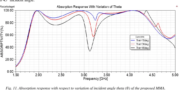
4.2.2 Incident wave variation
The structure has been simulated for different incident angle theta (𝜃). Fig. 11 depicts the absorption response with variation the incident angle (𝜃). As demonstrated in Fig. 11 the structure starts to create two bands within the wanted band. With the increase of incident angle, the lower and the higher frequencies are maintaining the same absorptivity response over the variation of incident waves. The variating in the absorptivity is in the middle of the band. However, it is absorbing most of the band up to 45° incident angle.
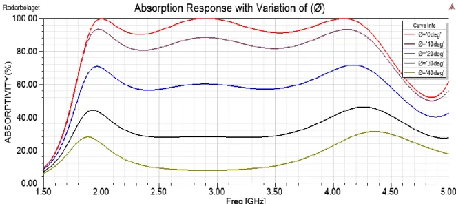
Moreover, variation in polarization angles (Ø) has also been studied. Fig. 12 illustrates the absorptivity response of the proposed structure under variation of polarization angle. The proposed structure exposed a broadband absorption up to 10˚ polarization angle with more than 80% absorptivity response.
5 Fabrication and experimental results
In this section the fabrication process followed to manufacture the single layer MMA discussed. The also section includes the measurement setup and the results of the fabricated 10×10 unit cells L-shaped single layer MMA. Moreover, the sensitivity of the fabricated MMA measured over variation of incident angles and variation of polarization angle was included.
5.1 Fabrication process
The proposed structure fabricated using printed circuit board (PCB) technology. Two L-shaped pattern array placed diagonally from each other was printed on the top side of 5.5 mm thickness FR-4 substrate board, with the bottom side fully etched up. Another 5.5 mm thickness FR-4 substrate board also used with a completely etched up face side and full copper plate on the bottom. The two etched sides were glued together to make the L-shaped pattern on the top of the 11 mm thickness FR-4, maintaining full copper lamination on the other side. The final structure dimensions are 300 ×300×11.07 mm, width, length and thickness respectively. Fig. 13 demonstrate the top view of (a) entire view and (b) the enlarge view of the proposed single layer MMA.
(a) (b)
5.2 Measurement setup
A pair of identical UWB antennas faced the proposed structure kept inside an anechoic chamber to measure the absorptivity of the fabricated structure. The two antennas were connected to Vector Network Analyzer (VNA) Rohde & Schwarz ZNB8. Moreover, port one was connected to the first antenna which is transmitting the electromagnetic waves. Port two was connected to antenna two which is receiving the reflected power from the fabricated MMA.
To measure the reflectivity and then the absorptivity of the fabricated single layer MMA, two measurements should be done. The power reflected from the copper plate back side of the fabricated MMA measured first as a reference (100% reflection) by measuring S21. Then, the power reflected from the L-shaped face side of the fabricated structure measured by also measuring S21. The difference between the reflected powers from the back and the face gives the exact reflected power from the fabricated MMA. And then the absorption equation can be applied on the difference in reflection to obtain the exact absorptivity of the structure.
The experiment setup including the fabricated proposed structure and the two antennas inside the chamber is shown in Fig. 14.
Fig. 14. Experimental arrangement within the anechoic chamber.
5.3 Absorptivity Response
The pair of the antennas put as close as possible to each other in order to minimize the incident waves angle as much as possible (close to 0°). The reflectivity of the back copper plate of the MMA was
power between the two signals taken and the absorption equation applied on the difference. Matlab has been used in order to subtract the signals and applying the absorption equation on the difference. The signals exported from the VNA and exported in to the Matlab. Therefore, Matlab has been used to plot the absorption response of the MMA.
A bandwidth of 1.69 GHz ranging from 2.23 GHz to 3.92 GHz with more than 90% absorption in the entire band except from 2.37 GHz to 2.53 GHz with 80% absorptivity response has been experimentally obtained. Fig. 15 demonstrates the absorptivity response of the fabricated MMA compared with the response of the simulated MMA. As presented in Fig. 15, the bandwidth of the fabricated structure is less than the simulated one. The difference in bandwidth between the fabricated and the simulated MMA responses is 350 MHz at the lower frequency, where its 400 MHz at the higher frequencies.
On the other hand, the fabricated MMA has more absorption peaks than the simulated structure. The peaks are; 99.96% at 2.63 GHz and 2.92 GHz, 99.7% at 3.1 GHz, 99.65% at 3.42 GHz, 99.99% at 3.65 GHz and 99.97% at 3.83.
The difference in absorption response and bandwidth between the fabricated and the simulated MMA response is due to fabrication tolerances and imperfection of measurement. That is, by using two antennas to measure the reflectivity of a surface it is impossible to measure 0° incident wave’s angle. The thickness error might also cause the difference, where the two 5.5 mm substrate glued together and the thickness is varying in some positions. Increasing of thickness has the ability to increase in absorption and reduce the bandwidth as discussed in the theory section.
The measurement of the fabricated L-shaped MMA discloses that the bandwidth of the simulated MMA is wider than the fabricated, and the absorption of the fabricated MMA is deeper than the simulated structure.
Fig. 15. Comparison between measured and simulated absorptivity responses of the proposed single layer MMA.
5.4 Variation of the Polarization Angle (Ø)
The structure has also been measured for different polarization angle (Ø). The polarization angle changed by rotating the pair of the antennas along its axis from 0° to 30°, with the step of 10° while the proposed structure was kept at fixed position. The reflectivity of the back copper plate measured first as a reference, then the face of the structure. The difference in the measured power between the face and the back taken at each polarization angle, and then the absorption equation applied on the measured difference. Fig. 16 depicted the comparison between simulated signal and measured signal of the single layer MMA over variation of (Ø). As shown in Fig. 16, the measured results matched the simulated results, where the absorption is decreasing in both; simulated and measured structure by increasing the polarization angle. The structure exposed a broadband absorptivity response up to 10° polarization angle with average absorptivity response more than 80%. Fig. 16(d) displays all the measured signals with respect of variation in (Ø) from 10° to 30° in one graph.
(a) (b)
(c) (d)
Fig. 16. Measured Absorption response with respect to variation of polarization angle (Ø) compared with its simulated response (a) Ø = 10° (b) Ø = 20° (c) Ø = 30° and (d) comparison for all measured Ø.
5.5 Variation of the Incident Angle (θ)
The structure measured over different incident angle (θ) to approve the simulation results. The change in theta (θ) has been obtained by changing the angle of the incident waves of the antennas with steps of 15˚, 30˚ and 45˚ while the structure was fixed. This obtained by changing the position of the antennas. The reflectivity of the back copper plate measured first as a reference, and then the reflectivity of the MMA face measured at each incident wave’s angle step. The difference in power was taken at each incident angle between the face and the back, then the absorption equation applied to calculate and plot the absorptivity of the proposed single layer MMA.
the measured fabricated structure response compared with the simulated response with the angle of incident waves is (θ) = 15°. The absorption response mostly is more than 90% except the range from 3 GHz to 3.32 GHz, where the response is ranging from 85% to 90%. The absorption bandwidth response with (θ) = 15° is 1.52 GHz ranging from 2.4 GHz to 3.92. Fig. 17 (b) illustrate the absorptivity of the measured structure with (θ) = 30°. Predominantly, the absorption response is more than 90% with exception of three narrow bands. The lower absorption frequency band within the wanted band is from 3.16 GHz to 3.35 GHz where the lowest response is 66% at 3.26 GHz. The absorption bandwidth response of the proposed structure with (θ) = 30° is 1.66 GHz ranging from 2.24 GHz to 3.9 GHz with mostly more than 90% absorption. Lastly, the absorptivity of the proposed structure measured with (θ) = 45° and the results compared with the simulated results depict in Fig. 17 (c). The absorption bandwidth is 1.6 GHz ranging from 2.32 GHz to 3.92 GHz. As can be seen from Fig. 17(c), the absorption response is lower than 90% from 2.55 GHz to 3.43 GHz with lowermost absorption response is at 2.94 GHz with 60%. Elsewhere, the absorption is higher than 90% with total bandwidth 1.6 GHz ranging from 2.32 GHz to 3.92 GHz.
Generally, the measured proposed MMA response, as the simulated response, started to create two bands within the bandwidth with the increase of the incident wave’s angle. The absorptivity of the fabricated structure reduced as the incident wave’s angle increased. The difference in absorptivity and bandwidth between the measured and the simulated response is due to the fabrication error and imperfection of measurements. The measurements error is because of the limitation of antennas movement inside the anechoic chamber room, and accuracy of measuring the angle of the incident waves.
(c) (d)
Fig. 17. Measured Absorption response with respect to variating of incident angle (θ) compared with the simulated response of (a) θ =15° (b) θ= 30˚ (c) θ= 45° and (d) comparison for all measured θ
It can be seen in some measured signals on the figures above, the absorption changes strongly with the frequencies below 2 GHz. That’s because of the wavelength of the frequencies lower than 2 GHz are much bigger than the size of the sample. Also the variation in distance between the antennas and the structure each angle step might cause the fluctuation in the absorption response for the frequencies lower than 2 GHz.
6 Conclusion and future work
This section is concluding and summarizing the entire report. It also contains the future work that can be done in order to improve the absorptivity response and size of the proposed single layer MMA.
6.1 Summary of results
In this report, designing, simulating, fabricating and testing of a single layer metamaterials absorber using in radar antenna housing to reduce the interference between the transmitter and the receiver antennas have been successfully obtained. The method used for the design succeeded to obtain the goal.
The designed MMA consists of three layers. Two metallic copper layers with thickness of 0.035 mm separated by FR4 dielectric with thickness of 11 mm. The top face of the structure is two L-shaped patches placed diagonally on the surface. The bottom surface is a completely copper plane separated from the top surface with dielectric. The simulated absorption bandwidth within the wanted band of the proposed MMA is 2.1 GHz with more than 90% absorptivity covering the S-band. The proposed single layer MMA has the ability to absorb most of the incident waves within the wanted band up to 45˚ incident wave’s angle. It also exposed a wide band response up to 10˚ polarization angle with more than 80% absorptivity. The structure was also studied under variation of dimensions, incident wave’s angle and polarization angle.
The proposed MMA fabricated with a cost of 4000 SEK. A 1.69 GHz bandwidth response ranging from 2.23 GHz up to 3.92 GHz was achieved. The structure can absorb most of the signals within the band up to 45˚ incident angle. The structure also exhibits wide bandwidth response up to 10˚ polarization angle with more than 80 % absorptivity. The fabricated MMA results followed the simulation results except the bandwidth. Where, the simulated MMA bandwidth of the absorption response is wider than the fabricated MMA.
6.2 Future work
The further work needed is to decrease the thickness of the structure and increase the absorption response bandwidth. This can be obtaining by changing all dimensions and size of the structure and produce more ground plane currents to contribute in the absorption process.
References
[1] N. I. Landy, S. Sajuyigbe, J. J. Mock, D. R. Smith, W. J. Padilla, ‘A Perfect Metamaterial Absorber.’ Phys. Rev. Lett. 2008, 100, 207402.
[2] K. Ling, M. Yoo and S. Lim. Frequency Tunable Metamaterial Absorber using Hygroscopicity of Nature Cork. IEEE Antennas Wirel. Propag. Lett. 2015, 14, 1598–1601.
[3] Chen, J., et al., “High-Impedance Surface-Based Broadband Absorbers With Interference Theory.” IEEE Transactions on Antennas and Propagation, 2015. 63(10): p. 4367-4374.
[4] Huang, L. and H. Chen, “Multi-band and polarization insensitive metamaterial absorber,” Progress In Electromagnetics Research, Vol. 113, 103–110, 2011.
[5] W. Ma, Y. Wen, X. Yu, “Theoretical and experimental demonstrations of a dual-band metamaterial absorber at midinferared,” IEEE Photonics Tech. Lett. Vol. 26, No. 19 (2014).. [6] Tao , H . et al. A metamaterial absorber for the terahertz regime: design, fabrication and
characterization . Opt. Express 16, 7181 – 7188 ( 2008 ).
[7] Y. Avitzour, Y. A. Urzhumov, and G. Shvets, “Wideangle infrared absorber based on a negative-index plasmonic metamaterial,” Phys. Rev. B, 79, 045131 (2009).
[8] K. Aydin, V. Ferry, R. Briggs, and H. Atwater, “Broadband polarization-independent resonant light absorption using ultrathin plasmonic super absorbers,” Nature Communications 2, 517 (2011).
[9] V. G. Veselago, Soviet Physics USPEKI 10, 509 (1968).
[10] M. Agarwal and M. K. Meshram, (2015, December). “X-band metamaterial absorber with dual band/broadband absorption characteristics’’ presented at the IEEE MTT-S International Microwave and RF Conference (IMaRC), 2015 (pp. 121-124). IEEE.
[11] J. B. Pendry, A. J. Holden, D. J. Robbins, and W. J. Stewart, “Magnetism from conductors and enhanced nonlinear phenomena”, IEEE Trans. Microwave Theory Tech., vol. 47, no. 11, pp. 2075–2084, November 1999.
[12] C. M. Watts, X. Liu, and W. J. Padilla, “Metamaterial electromagnetic wave absorbers,” Adv. Mater., vol. 24, no. 23, pp. OP98-OP120, June 2012.
[13] C. G. Hu, X. Li, Q. Feng, X. N. Chen, and X. G. Luo, “Investigation on the role of the dielectric loss in metamaterial absorber,” Opt. Express 18(7), 6598–6603 (2010).
[14] Liu , X . L . , Starr , T . , Starr , A . F . & Padilla , W . J . Infrared spatial and frequency selective metamaterial with near-unity absorbance . Phys. Rev. Lett. 104, 207403 ( 2010 ). [15] F. Bayatpur and K. Sarabandi, “Single-layer, high-order, miniaturizedelement frequency
[16] Wu, Kaimin, T. Wanghuang, Y. Huang, W. Chen and G. Wen, "Microwave metamaterial absorber with nλ 0/2 dielectric thicknesses." Communication Problem-Solving (ICCP), 2014 IEEE International Conference on. IEEE, pp. 79-82. 2014.
[17] S. Bhattacharyya et al. “A Broadband Wide Angle Metamaterial Absorber for Defense Applications” IEEE International Microwave and RF Conference. Bangalore (India), Diciembre 2014.
[18] CST Computer Simulation Technology: www.cst.com/, accessed date: August 2016. [19] ANSYS HFSS: www.ansoft.com/products/hf/hfss/, accessed date: February 2016. [20] Comsol Multiphysics: www.comsol.com/, accessed date: August 2016.
[21] HFSS: ‘Getting started with HFSS: Floquet ports’. [Online]. Available: http://www.ansoft.com , accessed Feb- 2016.
[22] T. Tomas and Z. Xiang. (2011, Dec).Perfect Lenses in Focus. Nature . 480, pp. 42-43. Available: http://www.nature.com
[23] Yang, H.; Cao, X.-Y.; Gao, J.; Yuan, W.; Li, Z.; Shang, K. Low RCS metamaterial absorber and extending bandwidth based on electromagnetic resonances. Prog. Electromagn. Res. M 2013, 33, 31–44.
[24] Pham, P. H. Q.; Burke, P.; Brown, E. Towards perfect impedance matching of free space to a 2D material. In 2014 44th European Microwave Conference, 1928–1930 (IEEE, 2014).
[25] W. S. Shaobin, B. Zhang, X. Kong, H. Zhang and S. Liu, “Broadband perfect metamaterial absorber based on flexible material,” presented at the IEEE International Workshop on Electromagnetics, Nanjin,May 16–18, 2016, Paper 10.1109/iWEM.2016.7505057.
![Fig. 1. Negative versus Positive refraction index [22].](https://thumb-eu.123doks.com/thumbv2/5dokorg/5437997.140507/14.892.322.565.694.924/fig-negative-versus-positive-refraction-index.webp)
![Fig. 2. Landy et al, metamaterial perfect absorber [1]](https://thumb-eu.123doks.com/thumbv2/5dokorg/5437997.140507/15.892.111.827.563.824/fig-landy-et-al-metamaterial-perfect-absorber.webp)