1
ON-BOARD PROTECTION DEVICE
FOR BATTERY CHARGER
SHEIDA POURSHAKOUR
ASHWINI UMARIKAR
School of Innovation, Design and Engineering
Level : A Supervisor: Hector Zelaya De La Parra Examiner: Prof. Lars Asplund Client: ABB AB Corporate Research
2
ABSTRACT
The goal of the thesis is to document the implementation of an On-board Protection Device that is to be used for On-board charging system in Electrical Vehicles.
On-board Protection Device is a protection part of the On-board charging system which communicates via CAN communication with the main charger unit. It includes basic fault detection hardware such as Ground Fault Monitoring, Residual Current Device and Main microcontroller for interface to and from peripheral fault monitoring devices and external communication networks. The Control logic is implemented inside a microcontroller, which also communicates with input channels and control output signals to circuit breaker which connects charger unit with supply. The microcontroller also send periodically the necessary data and status information about the peripheral protection devices to battery charger and also initiates close or open commands to circuit breaker, if there is any fault.
The thesis outlines the details of the protection device system design that can be helpful in utilizing or upgrading this system. The thesis is presented in two parts- The first part documents the design of Residual Current Device with 6mA leakage current and Ground Fault Monitoring device. The suggested solution is simulated by Pspice and is tested in the laboratory. The principle of protection devices is demonstrated through the experimental results. The second part documents the main logic part, implemented using TI Stellaris LM3S9B92 microcontroller, which has the required peripheral components to interface with different protection hardware and also has inbuilt CAN bus peripheral to communicate different CAN bus messages over CAN network. The control logic is first simulated in MATLAB using SIMULINK and STATEFLOW toolbox and then the actual implementation on the Evaluation Kit EKK-LM3S9B92 is described.
3
ACKNOWLEDGEMENT
We wish to express our sincere gratitude to our project supervisor from ABB, Dr. Hector Zelaya De La Parra for his exemplary guidance, support, monitoring and constant encouragement throughout the course of this thesis. We would also like to thank our supervisor and examiner Prof. Lars Asplund from Mälardalen University, for his helpful suggestions. And last but not the least we would like to thank our family for their constant encouragement and support without which this thesis would not be possible.
4
TABLE OF CONTENTS
1 INTRODUCTION ... 1 1.1 Purpose ... 1 1.2 Scope ... 1 1.3 Definitions ... 2 1.4 Structure... 3 2 PROBLEM DESCRIPTION ... 4 3 REQUIREMENTS ... 6 3.1 Hardware Requirements... 6 3.1.1 Power Supply ... 63.1.2 Ground Fault Monitoring ... 6
3.1.3 Residual Current Monitoring ... 6
4 SOLUTION ... 7
4.1 Hardware Design Overview... 7
4.2 Technical Specification ... 8
5 HARDWARE RESULTS ... 10
5.1 Simulation Result ... 10
5.2 Implementation Results ... 10
5.2.1 Test Result without Fault current ... 10
5.2.2 Test Result with 1mA Fault current... 11
5.2.3 Test Result with 2mA Fault current... 11
5.2.4 Test Result with 3mA Fault current... 12
5.2.5 Test Result with 4mA Fault current:... 12
5.2.6 Test Result with 5mA Fault current:... 13
5.2.7 Test Result with 6mA Fault current:... 14
5.2.8 Test Result with -6mA Fault current: ... 14
5.2.9 Tripping time with different waveforms: ... 15
5
6 SOFTWARE REQUIREMENT SPECIFICATIONS... 19
7 MICRO-CONTROLLER AND INTERFACE HARDWARE DESCRIPTION... 21
7.1 Stellaris family-LM3S9000 Series ... 21
7.2 Evaluation Kit EKK-LM3S9B92 ... 22
7.3 µVision IDE Keil ... 23
7.4 Microcontroller Peripheral ... 23
7.4.1 ADC ... 23
7.4.2 CAN ... 24
7.4.3 GPIO... 24
7.5 CAN module operation ... 24
7.5.1 CAN Specification ... 24
7.5.2 CAN Communication... 25
7.5.3 CAN bus operation ... 26
7.6 Flowchart of the protection device control logic ... 27
8 MICROCONTROLLER CONTROL LOGIC ... 30
8.1 Input output signal description ... 32
8.2 CAN implementation and CAN MSG specifications ... 33
8.3 Simulation of Protection device control logic ... 35
8.3.1 Simulink Representation ... 35
8.3.2 Protection device State machine implemented in Stateflow ... 39
8.3.3 MATLAB function "ChargerSim" ... 40
8.3.4 MATLAB function "Can decode" ... 43
8.3.5 MATLAB function "Can1 send decode" ... 45
9 HARDWARE IMPLEMENTATION... 47
9.1 Implementation Results ... 49
9.1.1 Wait state... 50
9.1.2 Precharging state ... 50
9.1.3 Charging state ... 50
6
9.1.5 Charging fail state ... 51
9.1.6 RCD trip limit set point change state ... 51
10 CONCLUSIONS ... 52
11 FUTURE WORK ... 53
12 REFERENCES ... 54
13 ENCLOSURES ... 55
1
1 INTRODUCTION
1.1 Purpose
The purpose of this report is to gather all information necessary to develop simulations and experimental implementations of an On-board protection device for electric vehicle battery charger.
Developing of the EV is beneficial both for saving energy and environment purposes. As to increase the use of EV, there is a need to consider a high degree of safety and reliability of electrical system compliant with the standards "CEN-CENELEC" that can protect the human life and reduce the danger of fire-risk.
On board battery chargers are commonly available in both EV and plug-in hybrid EV. The chargers are supplied from a single phase AC or a three – phase supply. Due to the relatively high power levels that are involved during charging, safety and protection of this operation is very important.
1.2 Scope
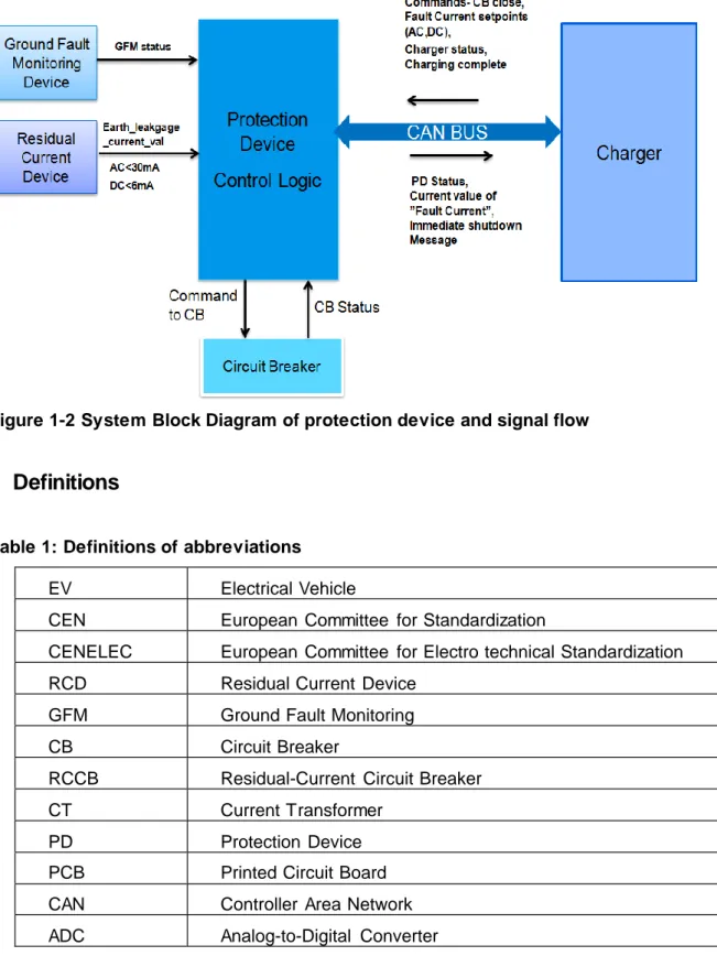
This report describes the Protection device for the battery charger. The protection functions of the device, described as shown in Figure 1-1, are RCD and GFM device. The commands from protection functions are interfaced a microcontroller. Microcontroller incorporates main control logic part which is responsible for processing on data coming from RCD or GFM and sending necessary information through the CAN bus to the battery charger. At the same time, if it detects any fault, the microcontroller also initiates necessary actions to disconnect the Circuit Breaker (CB) to disconnect charger from supply, thus preventing any further damages.
Figure 1-1: Electrical schematic of the electric vehicle
Figure 1-1 describes the protection device and its main components. The block diagram of overall system, as shown in Figure 1-2, Figure 1-2 also describes the communication requirements which are to be fulfilled by the protection device.
Leakage Current Protection
& Ground fault Monitoring Protection device
2
Figure 1-2 System Block Diagram of protection device and signal flow
1.3 Definitions
Table 1: Definitions of abbreviations
EV Electrical Vehicle
CEN European Committee for Standardization
CENELEC European Committee for Electro technical Standardization
RCD Residual Current Device
GFM Ground Fault Monitoring
CB Circuit Breaker
RCCB Residual-Current Circuit Breaker
CT Current Transformer
PD Protection Device
PCB Printed Circuit Board
CAN Controller Area Network ADC Analog-to-Digital Converter
3
1.4 Structure
This report has the following structure:
1. Introduction describes the purpose and scope for this report as well as terms, abbreviations and acronyms used.
2. Problem Description of the project.
3. The Project report is divided into two different parts: Part A: Hardware part
a. Hardware requirement
b. Hardware design and simulation c. Implementation and tests d. Result from hardware part Part B: Software part
a. Software requirement
b. Simulation and implementation c. Hardware implementation d. Result
4. Conclusion section 5. Future work
6. References (specify source material and further reading.) 7. Enclosures are supplementing information
4
2 PROBLEM DESCRIPTION
The main feature of the on-board battery charger is charging without using galvanic isolation so it reduces weight and price with higher efficiency. So in the event of any earth leaks, due to cables becoming damaged or water in the plugs etc. protection device is needed in order to trip the system or, in the events of short circuit, protection device will trip the unit to increase safety level of electrical equipment operation [1].
A protection device is working similar to a Residual-Current Circuit Breaker (RCCB). RCCB is an electrical wiring device that disconnects a circuit whenever it detects that the electric current is not balanced between the energized conductor and the return neutral conductor [2].
The protection device has to be design which includes basic fault detection hardware such as Ground fault monitoring, Residual current device and main microcontroller for interface to and from peripheral fault monitoring devices and external communication networks. The design of this RCD is similar to Type B (for every kind of earth current) [13] with ultra-sensitive tripping level current of 6mA leakage [14] [15]. The Printed Circuit Board (PCB) should be designed and tested. The Pspice simulation has to carry out to check the experimental result.
The Control logic has to design with a microcontroller, which also communicates with input channels and control output signals to circuit breaker which connects charger unit with supply. The microcontroller also send periodically the necessary data and status information about the peripheral protection devices to battery charger and also initiates close or open commands to circuit breaker, if there is any fault. The control logic has to be simulated first in MATLAB using SIMULINK and STATEFLOW toolbox and then the actual implementation will be done on the Evaluation Kit EKK-LM3S9B92.
5
6
3 REQUIREMENTS
On board protection device is a protection system which is divided into two major parts, hardware and software. Hardware part includes the design of protection device that can detect the leakage current and ground fault.
3.1 Hardware Requirements
In order to fulfill the requirement of the protection device, hardware design includes the following parts:
3.1.1 Power Supply
Two different levels of voltages, +14V and -6V, are supposed power to feed to the protection device. For a microcontroller, in control logic part, the required power is 3.3V and all other comparators and amplifiers need ±6. A DC-DC converter is needed to convert 14V to 3.3V and +6V.
3.1.2 Ground Fault Monitoring
In order to increase safety and reliability for On-board charging process of an EV, a control circuit is needed to take into consideration. The Ground Fault detecting circuit is responsible for checking continuously proper connection between car chassis and ground. 3.1.3 Residual Current Monitoring
The main functionality of protection device is detecting the leakage current, 6mAdc and 30
mAac with different waveforms. A residual current device is needed to detect the leakage
7
4 SOLUTION
4.1 Hardware Design Overview
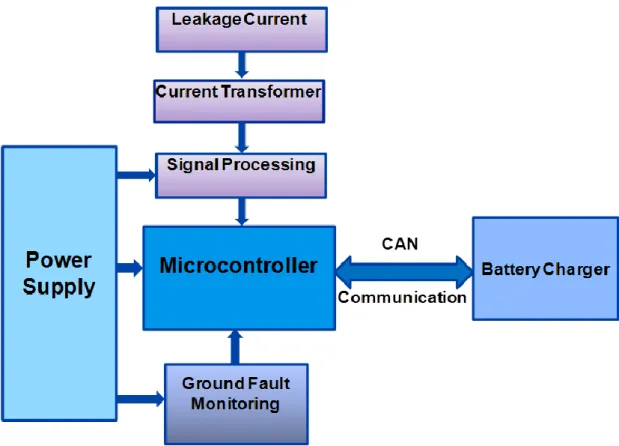
In order to meet the requirements of a protection device ,the main features of device should include measuring of the leakage current, check the ground connection, control the output signals and sending them through the CAN bus Figure 4-1. The schematic of suggested design over each part is attached in section 13.
8
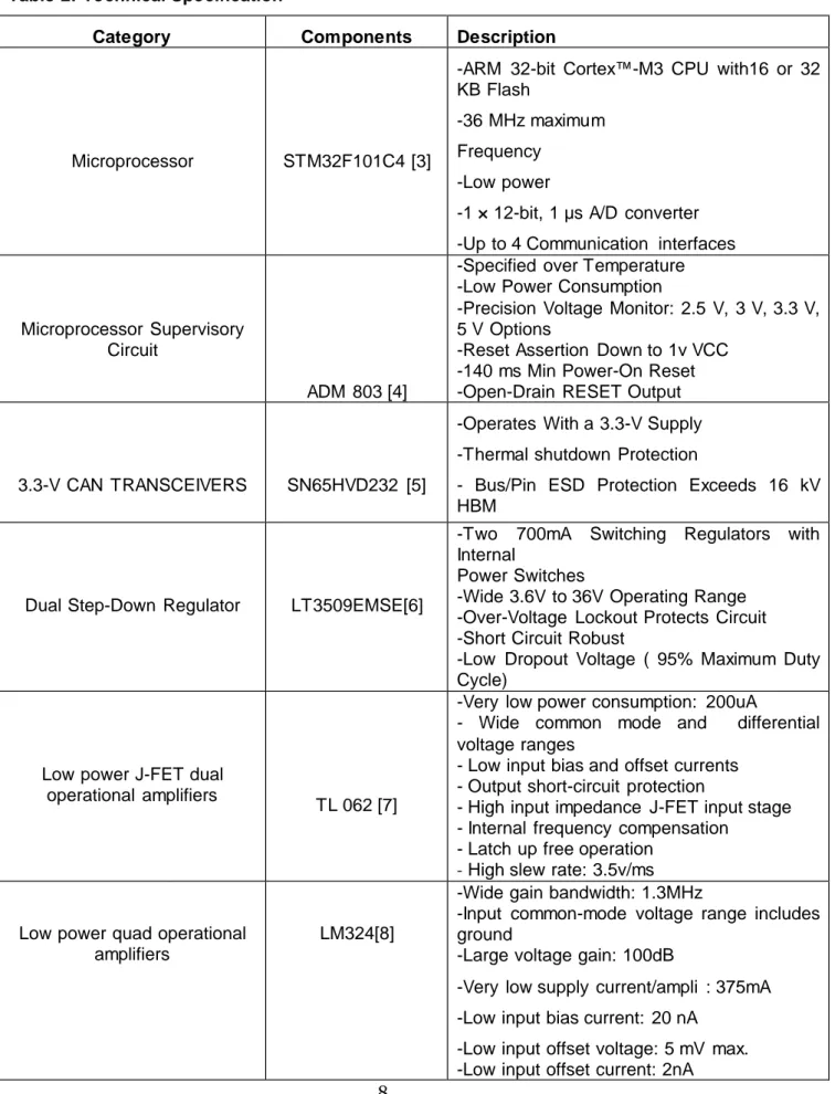
4.2 Technical Specification
Technical specification of the final prototype is gathered in the following table.
Table 2: Technical Specification
Category Components Description
Microprocessor STM32F101C4 [3]
-ARM 32-bit Cortex™-M3 CPU with16 or 32 KB Flash
-36 MHz maximum Frequency
-Low power
-1 × 12-bit, 1 μs A/D converter -Up to 4 Communication interfaces
Microprocessor Supervisory Circuit
ADM 803 [4]
-Specified over Temperature -Low Power Consumption
-Precision Voltage Monitor: 2.5 V, 3 V, 3.3 V, 5 V Options
-Reset Assertion Down to 1v VCC -140 ms Min Power-On Reset -Open-Drain RESET Output
3.3-V CAN TRANSCEIVERS SN65HVD232 [5]
-Operates With a 3.3-V Supply -Thermal shutdown Protection
- Bus/Pin ESD Protection Exceeds 16 kV HBM
Dual Step-Down Regulator LT3509EMSE[6]
-Two 700mA Switching Regulators with Internal
Power Switches
-Wide 3.6V to 36V Operating Range -Over-Voltage Lockout Protects Circuit -Short Circuit Robust
-Low Dropout Voltage ( 95% Maximum Duty Cycle)
Low power J-FET dual operational amplifiers
TL 062 [7]
-Very low power consumption: 200uA
- Wide common mode and differential voltage ranges
- Low input bias and offset currents - Output short-circuit protection
- High input impedance J-FET input stage - Internal frequency compensation
- Latch up free operation - High slew rate: 3.5v/ms
Low power quad operational amplifiers
LM324[8]
-Wide gain bandwidth: 1.3MHz
-Input common-mode voltage range includes ground
-Large voltage gain: 100dB
-Very low supply current/ampli : 375mA -Low input bias current: 20 nA
-Low input offset voltage: 5 mV max. -Low input offset current: 2nA
9
-Wide power supply range: Single supply: +3V to +30V -Dual supplies: ±1.5V to ±15V Precision Rail-to-Rail Comparator LT1716 [9] -Operates from 2.7V to 44V -Micro power: 35μA IQ -Offset Voltage: 1.5mV Max
-Valid Output with Either Input 5V Below V– - Rail-to-Rail Output Swing
-Output Can Drive Loads Above V+ - Internal Pull-Up Current
- –40°C to 125°C Operating Temperature Range
10
5 HARDWARE RESULTS
The results of simulation and test the designed circuit are shown in following figures.
5.1 Simulation Result
The simulation of circuit, with different fault current 1, 2, 3, 4, 5 and 6 mA dc, is achieved by Pspice and is shown in Figure 5-1.
Figure 5-1: Simulation Result of Different Fault current
As is shown in Figure 5-1 when there is no fault offset voltage is about 1.4V. With increasing the leakage current output voltage increases. The maximum value reached by 6mA leakage current is almost 3.7V.
5.2 Implementation Results
In the laboratory, designed circuit is tested and following result is recorded by oscilloscope with different fault currents.
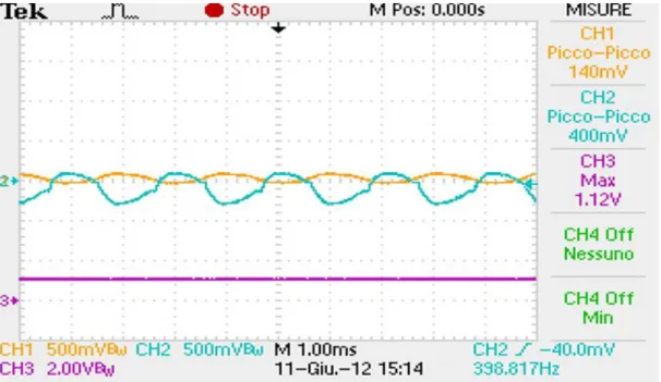
5.2.1 Test Result without Fault current
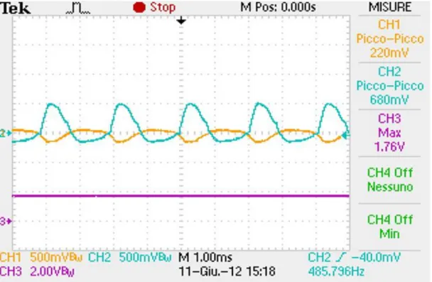
As is shown in the figures, channel 1 shows the voltage after first amplifying, channel 2 shows the second inverted amplified voltage and channel 3 is the output voltage. When there is not any fault current output voltage is 1.12V.
11
Figure 5-2: Test Result without Fault current
5.2.2 Test Result with 1mA Fault current With 1mA fault current output voltage is 1.28V.
Figure 5-3: Test Result with 1 mA dc Fault Current
5.2.3 Test Result with 2mA Fault current
12
Figure 5-4: Test Result with 2 mA dc Fault Current
5.2.4 Test Result with 3mA Fault current
The output voltage reaches 2.40V when the fault current is 3mA.
Figure 5-5: Test Result with 3 mA dc Fault Current
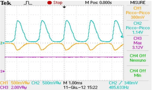
5.2.5 Test Result with 4mA Fault current: With 4mA fault current, output voltage is 3.12V.
13
Figure 5-6: Test Result with 4 mA dc Fault Current
5.2.6 Test Result with 5mA Fault current:
The output voltage increases to 3.76V when the current reaches 5mA.
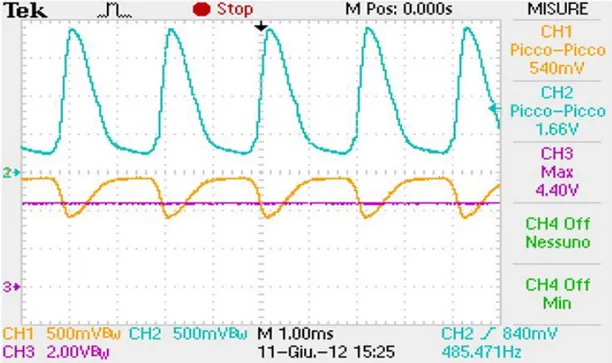
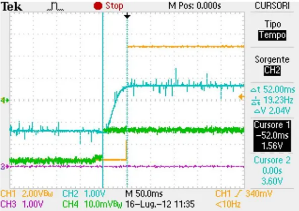
14 5.2.7 Test Result with 6mA Fault current: The tripping voltage that is equal to 6mA is 4.40V.
Figure 5-8: Test Result with 6 mA dc Fault Current
5.2.8 Test Result with -6mA Fault current:
All the test situations are repeated with minus current value. The tripping voltage values show almost the same as the plus fault current values. Figure 5-9 shows the tripping value with -6mA.
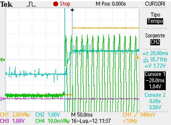
15 5.2.9 Tripping time with different waveforms:
Tripping time of the On-board protection device in different frequencies is measured and recorded. All recorded results are shown in the following figures.
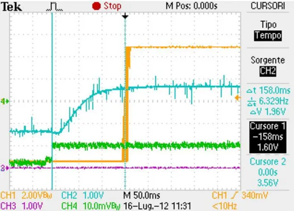
A. Tripping time with pulse waveform in low frequency (f=6.329Hz):
Figure 5-10: Tripping time with pulse waveform in low frequency
16
Figure 5-11: Tripping time with pulse waveform in middle frequency
C. Tripping time with pulse waveform in higher frequency (f=38.46Hz):
Figure 5-12: Tripping time with pulse waveform in higher frequency
17
The result of tripping time with AC waveform is shown in the next figure.
Figure 5-13: Tripping time with AC waveform at 30maac
5.2.10 Threshold current with different waveforms:
All threshold current results with different waveforms are gathered in table which is shown below.
18
19
6 SOFTWARE REQUIREMENT SPECIFICATIONS
On board protection device is a protection system which is divided into two major parts, hardware and software. Details about different fault sensors like RCD, Ground monitor device etc are described in Part I. This part or the report is deal with the microcontroller hardware, different functions associated with it and the implementation of the control logic for protection device..
The functional requirement for controller are mainly the design and implementation of the control logic related to communications of status signals from peripheral protection functions and CAN bus communications to the charger unit . Figure 6-1 describes the overall Protection device and Charger system along with different signal flow paths. The status signals from Ground monitor device and Residual current device are input to the coming to the microcontroller unit of the Protection device. The Protection device will check these inputs, if there is any fault detected by the peripheral devices, microcontroller will not send "close CB" command to circuit breaker, preventing the charger unit to start charging process, otherwise it will close the circuit breaker and send corresponding message to Charger about no fault detected by peripheral protection devices and starting the charging process. The Protection device communicates continuously with peripheral devices to check for faults based on the input from the devices GMD and RCD, and send corresponding message to Charger about the status (Fault or No fault). The microcontroller unit also receives messages from charger through the CAN bus. The different messages being received through CAN bus are operation commands like charging process start, stop commands, leakage current set points, etc, as shown in Figure 6-1 All these message communication between Protection device and Charger is done using CAN, the details of CAN bus communications are described in details in section 7.4.2
Figure 6-1: System block diagram
The microcontroller functions are thus summarized as below
- Configuration of ADC channels to interface with analog input signals from RCD hardware like residual leakage current detector- both AC and DC currents.
- Interface GPIO ports- CB close/open command output and CB status monitoring, Status monitoring from Ground fault monitor device
Protection Device Control Logic Circuit Breaker Charger Ground Monitoring Device Residual Current Device GMD status Command to CB CB Status Commands- CB close, Fault Current setpoints (AC,DC), Charger status, Charging complete PD Status, Current value of ”Fault Current”, Immediate shutdown Message Earth_leakgage
_current_val CAN BUS
AC<30mA DC<6mA
20
- CAN bus communications with Charger unit. Configuration of CAN bus to communicate various messages with charger for communication.
- control logic including Intelligent state machine to control CB based on status of peripheral fault sensing devices as well as commands received from charger
Figure 6-2: Software process flow
Part II of report is based on the above aspects of control functions, the different chapters in Part II are organized in following fashion.
- Chapter7deals with selection of microcontroller with required functionalities and brief description of selected microcontroller.
- Chapter 8 presents the overall control logic, various CAN message specifications. The simulation of Protection device logic using Simulink MATLAB is also presented in this chapter.
- Chapter 9describes the actual implementation of the control logic on the prototype microcontroller board and presents the sample results
21
7 MICRO-CONTROLLER AND INTERFACE HARDWARE
DESCRIPTION
The basic requirements for the selected microcontroller are listed as - It should have low supply voltage range (1.8V to 3.6V).
- It should be low cost.
- It should have internal CAN peripheral.
- It can be used for serial onboard programming, no external power supplies needed for programming.
- It should be able to use for an automotive application.
As described above, the microcontroller should have certain functionality within. The selection of the microcontroller is based on considering all the requirements and design. The requirements and some advanced features of microcontroller lead to selection of the Stellaris family from TI, i.e. Stellaris ARM cortex-M3 microcontrollers. The Stellaris family combines sophisticated, flexible, mixed signal system on chip integration. It provides unparalleled real time multitasking capabilities. Also it is cost effective and simple to program.
As considering the requirements, the Microcontroller should have CAN peripheral within, and Stellaris microcontroller from family series 9000 provides this feature with some more advanced features. The microcontroller LM3S9B92 has some advanced features which are not required for our project. The main requirement from microcontroller is CAN and ADC functionalities.
7.1 Stellaris family-LM3S9000 Series
22
Texas Instruments’ LM3S9000 Series features an on-chip combination of 10/100 Ethernet MAC/PHY, USB On-The-Go/Host/Device, and Controller Area Network (CAN). In addition to several product enhancements, the LM3S9000 Series adds new features, such as a versatile External Peripheral Interface (EPI) with modes to support SDRAM, SRAM/Flash, Host-Bus, and M2M, an Integrated Interchip Sound (I2S) interface, simultaneous dual ADC capability, a second watchdog timer with independent clock for safety critical applications.
7.2 Evaluation Kit EKK-LM3S9B92
Figure 7-2: Evaluation board LM3S9B92 and In-circuit debug interface board
The EKK-LM3S9B92 evaluation kit is used for first prototype. This kit has two boards Evaluation board and In-Circuit debug interface (BD-ICDI) board.
Features of evaluation board:
- It has LM3S9B92 high performance Stellaris microcontroller and large memory o 32 bit ARM Cortex-M3 core
o 256 KB single cycle Flash memory o 96 KB single cycle RAM
- It also has a 10/100 Mbit Ethernet port. - A full speed USB-OTG port
- Virtual serial communications port capability - Detachable ICDI board
23
7.3 µVision IDE Keil
Figure 7-3 Keil IDE
µVision IDE from Keil is used for the source code editing and program debugging. This IDE is provided with the Evaluation kit. This µVision IDE by Keil is easy to use for creating embedded programs that works. The µVision editor and debugger are integrated in a single application that provides a seamless embedded project development environment.
7.4 Microcontroller Peripheral
The main peripherals of Stellaris LM3S9B92 microcontroller are as shown in Figure 7-1. Only the peripherals on interest to the project specifications are described in this section, these are ADC channels and related interface, CAN bus, General purpose I/O (GPIO) 7.4.1 ADC
An analog-to-digital converter (ADC) is a peripheral that converts a continuous analog voltage to a discrete digital number. The Stellaris LM3S9B92 microcontroller has two identical converter modules. These ADC modules support 10-bit conversion resolution, 16 input channels and an internal temperature sensor. Each module contains 4 programmable sequencers allowing the sampling of multiple analog input sources without controller intervention [10]. Four sampling sequencers, has configurable trigger events which can be captured. The first sequencer captures up to eight samples, second and third captures up to four samples and the fourth sequencer captures single sample. Each sample can be the same channel, different channels or any combinations in any order. (For additional detail refer [10]&[11])
24 7.4.2 CAN
Controller Area Network (CAN) is multicast, shared serial bus for connecting electronic control unit (ECU’s). Stellaris LM3S9B92 microcontroller includes two CAN units with following features,
CAN protocol version 2.0 part A/B Bit rates up to 1 Mbps
32 message objects with individual identifier mask
Programmable FIFO mode enables storage of multiple message objects
Gluelessly attaches to an external CAN transceiver through the CANnTX and CANnRX signals[10]
The Stellaris CAN module provides hardware processing of the CAN data link layer. It can be configured with message filters and preloaded message data so that it can autonomously send and receive messages on the bus and notify the application accordingly. It automatically handles generation and checking CRCs, error processing and retransmission of CAN messages [11].
These CAN modules can be configured with message filters and preloaded message data so that they can autonomously send and receive messages on the CAN bus and notify the application accordingly. The message objects are stored in the CAN controller and provide the main interface for the CAN module on the CAN bus. The Message object can be programmed to handle a separate message ID or can be chained together for a sequence of frames with the same ID. The message identifier filters provide masking that can be programmed to match any or all of the message ID bits and frame types. (For additional detail refer [10]& [11]).
7.4.3 GPIO
The GPIO module of Stellaris LM3S9B92 microcontroller is consist of nine physical GPIO blocks, each corresponding to an individual GPIO port (Port A, Port B, Port C, Port D, Port E, Port F, Port G, Port H, Port J). The GPIO supports up 65 programmable input/output pins, depending on the peripheral being used [10] & [11].
The GPIO pin can configure to be GPIO or peripheral pin. Not all pins on all part have peripheral function; in this case pin can be only used as a GPIO [10]& [11]. The GPIO pins are specified using bit packed byte, where each bit that is set identifies the pin to be accessed. Bit 0 represents GPIO port pin 0, bit1 represents GPIO port pin 1, bit 2 represents GPIO port pin 2 and so on[11].(For additional detail refer [10]&[11]).
7.5 CAN module operation
7.5.1 CAN SpecificationThe CAN messages, from Charger or from Protection device are the message with some specific data as well as Identification (Message ID). For some specific message these CAN message ID’s are assigned. Message transfers that includes data, remote, error and overload frames with an 11 bit identifier (standard) or 29-bit identifier (extended) are supported. The CAN data frame contains data for transmission. The remote frame does not contain any data; it is used for requesting the transmission of specific message object. The data frame is constructed as shown in following Figure 7-4 : CAN data/remote Figure 7-4 [10].
25
Figure 7-4 : CAN data/remote frame [10]
7.5.2 CAN Communication
CAN is a multicast, shared serial bus standard for connecting electronic control units (ECU’s). CAN was specifically designed to be robust in electromagnetically-noisy environment. It’s created originally for automotive purposes, but also used in many embedded control applications. For the network lengths of less than 40 it can provide bit rate up to 1Mbps.
The Stellaris CAN controller conforms to the CAN protocol version 2.0(parts A and B). It has bit rate up to 1Mbps. It has 32 message objects with individual identifier mask. And it gluelessly attaches to the an external CAN transceiver through the CANnRX and CANnTX The Stellaris LM3S9B92 has two CAN modules, each CAN module consist of three major parts
1. CAN protocol controller and message handler 2. Message memory
3. CAN register interface
The Protocol controller transfers and receives the serial data from CAN bus and passes the data onto the message handler. The message handler loads this data into appropriate message object. The message handler is also responsible for generating interrupts based on events on the CAN bus.
The message memory is set of 32 identical memory blocks that hold the current configuration, status, and actual data for each message object. These memory blocks are accessed via either of the CAN message object register interfaces.
The Stellaris CAN controller provides an interface to communicate with the message memory via two CAN interface register sets for communicating with the message objects, as the message memory is not directly accessible. These two interfaces must be used to read or write to each message object [10]. The two message object interface allows parallel access to the CAN controller message objects when multiple objects may have new information that must be processed. Here one interface is used for transmit data and one for receive data
26 7.5.3 CAN bus operation
Mainly CAN bus operation includes the transmitting and receiving the DATA to and from the CAN bus.
Sequence of transmitting data on CAN bus [12]:
If the CAN bus is idle, any node can start sending CAN frame. All other node will receive it.
There is priority process, which will decide the priority of the node. The node with highest priority will transmit first. The nodes with less priority will stop transmitting and start receiving. After transmitting the frame the node will wait for one bit time for the acknowledgement (ACK)
bit to be set, which is the indication of that some node has received it.
If it the acknowledgment (ACK) bit is not set then, this node will resend the fame as soon as possible.
Now all nodes again start to send their CAN far over the CAN bus. Sequence of receiving data on CAN bus [12]:
All nodes except those currently transmitting frames are in listening mode. The CAN frame is transmitted as described above.
The frame is received by all other nodes, if deemed to be a valid CAN message an acknowledgment (ACK) bit is set.
The frame is then sent through controller’s acceptance filter mechanism. If this frame is rejected it will get discarded otherwise it is sent to controller FIFO memory. If the FIFO is full the old frame is lost.
The host processor gets alerted to the fact that a valid frame is ready to be read from FIFO. This frame must be read as soon as possible.
The host processor takes decision about what to do with message as determined by software. Following are the steps for CAN operation from defining till sending the message [10].
1. Define the CAN message object.
2. Configure GPIO port to utilize its CAN function. 3. Initialize CAN controller.
4. Set up bit rate for the CAN bus.
5. Enable interrupts on the CAN peripheral. 6. Enable CAN interrupt on the Processor. 7. Enable CAN for Operation.
8. Initialize the CAN message object for sending and receiving messages.
9. Load the message object into the CAN peripheral, once loaded the CAN will receive any message on the bus and an interrupt will occur.
10. Check for the logical condition and set the CAN message ID. 11. Send the CAN message over the CAN bus.
Steps 1-7 are executed during the initialization phase of the microcontroller logic, whereas steps 9-11 are repeated in a loop of the main control logic.
27
7.6 Flowchart of the protection device control logic
Based on the software requirement specification as described in chapter 6and the microcontroller and its peripherals described in section 7.1 and 7.4, the flowchart of the different decision making process in microcontroller is prepared which is describes in this section.
The overall control logic will have following sections 1. Initialization section
The initialization section includes the declaration and initialization of different variables, enabling the peripherals followed by the setting the GPIO port and pins for the required operation like ADC, CAN or just as GPIO input or output.
2. Main Control Logic section
The main control logic includes, reading the input values and depending on these input values design the logic. In detail it follows some steps as,
a. Receiving and decoding of CAN messages.
b. Check for the faults from the peripheral devices- Residual current device and Ground monitor device.
c. Setting control logic flags accordingly.
d. Take actions specific to closing/opening of CB
e. Encoding CAN messages and sending messages over CAN
The initialization part is executed at the start of the program only, afterwards the main program executed in the loop.
28
Figure 7-5: Main program structure
Start Define and
Iniatialize parameters CAN Interrupt handler
Enable the Peripheral CAN,ADC
GPIO Port and Pin setting
ADC Configuration
CAN Configuration
Main Control Logic, State machine
Read ADC values Read input value from IO ports, CAN
messages
Main Program
Output DOs to output ports, CAN messages
Initialization section
29
Figure 7-6: Flowchart of main control logic
Check Ground fault, Earth leakager current fault,
If Fault? Setting Fault flags Yes
No
Control Logic
Receive & Decoding CAN bus MSG’s
Send CAN bus MSG’s PD status, Fault flags
GPIO actions CB, Status display
30
8 MICROCONTROLLER CONTROL LOGIC
The software task of the project is to implement the software as per the system requirement specifications described in chapter 6, which are also elaborated by the flow chart presented in section 7.6. The performance testing and verification of the control logic needs that all peripherals are present and communicate with the microcontroller. Another requirement is that the CAN network is available and the CAN MSGs from charger are available. Thus to design the control logic for protection device, a dedicated charger hardware (CAN communications part) is required for the signal (messages) communication. As during the project stage, it is practically not possible to get the charger for checking the control logic of protection device, the following alternate system, as shown in Figure 8-1, is proposed, which is different from the original system requirement specifications.
Figure 8-1: System proposed using two CAN modules
1. The Stellaris LM3S9B92 microcontroller has two CAN modules, using these two CAN modules, the system with Protection device and Charger is simulated. The same microcontroller now also performs operation of CAN signal generation of charger.
2. The chargers states, which are transmitted over CAN network, are generated using two digital input signals S1 and S2. The microcontroller thus incorporates a simple decode logic which generates the charger states based on digital I/O status.
3. The 0 or 5 V is fed to the GMD status input to simulate the GMD status.
4. A resistor- switch (two pole switch) pair is used to generate 0 or 5 V depending upon position of the switch. A number of these networks are used to generate the different status signal needed for logic simulation. A LED is connected to the input pins to indicate status of input signals as shown in Figure 8-2.
S8 E5
Command to Circuit breaker
PD Status, Current value of ”Fault Current”, Immediate shutdown Message Control Logic Charger (Encode logic) Decoder / Encoder EKK-LM3S9B92 S1 E0 Charger status1 S2 E1 Charger status2 S6 F4
Ground monitoring device
S3 E6
Set point command
S7 B6
Circuit breaker status CAN
Transceiver CAN Transceiver Commands- CB close, Fault Current set points (AC,DC), Charger status, Charging complete CAN1 CAN0 F0 F1 A7 A6 C A N B U S 0 - 3V E2 ADC1 S5 Protection device fault status
31
Figure 8-2: Digital, analog input signal generation and output signal indicators
5. An analog voltage reference with variation between 0-3V used as earth leakage current input. This is done since the actual RCD hardware was not ready at the time of microcontroller implementation. But the RCD input can be directly connected to the same port with proper scaling as shown in Figure 8-3. The example values shown in Figure 8-3 are with the setting of 7mA RCD current input, which is converted equivalent voltage of 2.94 V, the ADC input voltage range is between 0-3V.
6. The output from the control logic- PD status and charging status is interfaced with two digital i/Os configured as output- S5 and S8 as shown in Figure 8-2. LEDs are connected at the digital input and outputs for visual information of various digital inputs and output.
Figure 8-3: ADC interface for actual leakage current signal from RCD
The later part of this chapter is arranged as following,
- First, the various digital input and output signals are described in section 8.1.
- Then the CAN specifications are described in section 8.2 with actual CAN message IDs and DATA for various conditions, the specifications include the CAN MSGs from both charger and protection device.
5V
S1 S2 S3 S4 S5 S6 S7 S8GND
R1 R1 R1 R1 R1 R1 R2 R2 R2 R2 R2 R2 R2 R2L1
L2
L3
L4L5
L6
L7L8
R1= 550 ΩR2= 1.1kΩ
2R 3R ADC1420 ohm,
From RCD
7mA
To ADC Channel
2940 mV
32
- Section 8.3 presents the simulation of the complete logic along with the simulation results. The complete logic is simulated on MATLAB-SIMULINK software platform whereas the state machine is implemented using STATEFLOW toolbox.
- Finally the actual implementation of the logic on the Stellaris EKK-LM3S9B92 evaluation board is described in section 0.
8.1 Input output signal description
The table below lists the various digital input and output signals used in the implementation. As described in above section, the digital status signals from various peripherals are simulated by 2 pole switches which can connect to either 5V or GND, thus generating either 1 or 0 state (Figure 8-2) Similarly, analog voltage input equivalent to earth leakage current is simulated by using a potentiometer with variable voltage from 0 to 3 V (maximum allowable input voltage for ADC channels is 3V). The output signals from the microcontroller are connected to LEDs for status indication. Table 4 describes the details about these signals along with the port numbers on evaluation board where these signals are connected.
Table 4: Input signal table
Signal Name From To Type
Port-pin numbe r Switch /ADC input Range Description Earth_leakag e_current_val Residual current device Protection device
Analog E2 ADC1 0-3 V Earth_leakage_curre nt_val<6mA or 30mA: No Fault Earth_leakage_curre nt_val>6mA or 30mA : Fault GMD_status Ground Monitor Device Protection device
Digital F4 S6 0 to 1 GMD_status = 0 :No Fault GMD_status=1: Ground Fault CB_status Circuit Breaker Protection device
Digital B6 S7 0 to 1 CB_Status=0 : Open Circuit CB_Status=1 : Close Circuit Charger status 1 Charger Protection device
Digital E0 S1 0 to 1 Combination of two status signals "S2S1" are used to generate 4 charger status states- "00"-charging wait, '01'-charging start, '10'- charging, '11'-charging complete Charger status 2 Charger Protection device Digital E1 S2 0 to 1 Set point enable Charger Protection device Digital E6 S3 0 to 1 0: No Change 1: Change the current trip level Set
33
Table 5: Output signal table
Signal Name From To Type Po rt LED Ran ge Description PD_status Protection device Charger Digita l E4 LED1 0 to 1 0: No fault continue charging 1: Fault detected by PD, stop charging Command_t o_CB Protection device Circuit breaker Digita l E5 LED2 0 to 1 0: Open Circuit 1: Close Circuit
8.2 CAN implementation and CAN MSG specifications
As described above and shown in Figure 8-1, the protection device control logic as well as charger CAN bus messages are implemented using the two CAN modules in Stellaris LM3S9B92 evaluation board.
CAN bus module CAN0 is configured to send Charger messages, these messages are generated using combination of the digital inputs as described in Table 4. Similarly, the generation of CAN bus messages to be send from Charger are also generated first at the beginning of main control logic and are sent using CAN0 module. CAN1 module is considered as Protection device. Protection device part of the logic receives the information from charger by decoding the CAN messages which are received by CAN1. CAN1 also transmits the information sent from protection device using the CAN1 module. CAN bus messages have unique IDs and data for sending different signal information between charger and protection device. These signal information are listed in Table 6. The Process will start with the CAN message for closing the circuit breaker from Charger to Protection device. The Protection device will then check for occurrence of fault in any of the devices (GMD and RCD). If GMD fault is there it will send message of immediate shutdown to the Charger. If RCD fault is arise, it will send the immediate shutdown message as well as it will send the current value of “fault current” to the Charger. If there is no fault then it will send the message of status of Protection device to the Charger. In between the Charger will send the message about its status. When the process of charging is over, The Charger will send the message as charging complete to the Protection device and the Protection device will open the circuit breaker. If there is change in the trip level value of current then the Charger will send the message with new set point values of fault current for both AC and DC. Following table summarizes these CAN messages referring to
Table 6: CAN messages
CAN messages from Charger CAN messages from Protection device
Close the circuit breaker Protection device status
Charger status Immediate shutdown
Charging complete Current value of fault current
Fault current set point value
34
Following Table 7 describes the Message ID and the data it contains with interpretation as well as description. The message contains 8 bytes of data. The first table summarizes the CAN messages send from protection device to the Charger and Table 8 lists the collective messages coming from Charger to the Protection device with MSG IDs and its data content.
Table 7: Messages from protection device to Charger
MSGID Interpretation Data
byte0 Data byte1 Data byte2 Data byte3 Description 0x0FF Immediate
shutdown 0x5C Current below
threshold
0X01 AC fault
current detected
any other DC fault
current detected 0x120 Current value of fault current AC DC As read by ADC input channels 0x131 status of PD for charger state PD State machine status
In the present implementation, the bytes 1 to 3 are left default for MSG id 0x0FF. Similarly since only one ADC input is used in present implementation which is treated as AC current input, the DC current input value in byte 2 and 3 for MSG id 0x120 is left default. Similarly byte 1 to 3 for MSG id 0x131 is unused. The priority of different messages is as below
- The MSG 0x131 is transmitted continuously in normal operation.
- In the event of fault, the highest priority MSG 0x0FF is transmitted once (this message has information about trip action because of fault detected by protection device).
- This MSG is followed by 0x120, which contains the information about fault current values.
- After this, again message 0x0131 is transmitted continuously as before.
Table 8 : Messages from Charger to protection device
MSG ID Interpretation Data
byte 0
Data byte 1
Data byte 2,3 Data byte 4,5 Data byte 6,7 0x130 charger status for PD 0x00 disconnected from power grid value of compensated fault current value of RMS current drawn from value of RMS voltage of power 0x01 connected to grid - inrush 0x02 connected to
35
grid - charging power
grid grid 0x03 connected to grid - not charging 0x00 no compensation necessary 0x01 compensation in progress 0x2x compensation exceeded limits 0x320 fault current set points AC DC
In the present implementation, the bytes 1 to 7 are left default for MSG id 0x0FF; this is done since actual charger is not present. Instead, as explained earlier in Table 4, combination of S1 and S2 switches is used to generate one of four charger states being transmitted in byte 0 of MSG id 0x0FF. Similarly since only one ADC input is used in present implementation, only one Set point value (AC in byte 0 and 1) is used in MSG id 0x320. The priority of different messages is as below
- The MSG 0x130 is transmitted continuously in normal operation.
- In the event of fault current value setting, MSG ox320 is transmitted. (this message has information about AC fault current trip level)
- After this again message 0x0130 is transmitted continuously as before.
8.3 Simulation of Protection device control logic
The control logic shown in described in Figure 8-1 is simulated using the MATLAB. The main logic is simulated in Simulink environment whereas the main control state machine is simulated using the Stateflow toolbox.
8.3.1 Simulink Representation
Figure 8-4 shows the main block diagram of the overall control logic in Simulink. The Protection device module is consist of Stateflow module as control logic, an embedded MATLAB function block is used as a decoder block, which will decode the CAN messages coming from the Charger and Similarly other embedded MATLAB function block is used for encoding the CAN messages from messages from Protection device which are transmitted to the Charger.
The various inputs to the control logic are simulated as equivalent low or high inputs. These include status signals from Ground fault monitoring device, circuit breaker, etc. The analog input signal like RCD current and set point value are generated using slider gain blocks in Simulink. A slider gain is used to provide input through this signal as it is representing threshold value which is varying from 0mA to 6mA. The digital output signals are connected to scope and displays for monitoring. Stateflow used to show the control logic part in the Simulink. Similar to the actual implementation, the simulation also include encode and decode logic blocks associated with CAN bus. The CAN bus messages can be viewed using scopes connected to CAN bus. The encoder and decoder logic for CAN 0 and CAN1 module is implemented using simple MATLAB function blocks.
The protection device gets commands from Charger through CAN bus to start the charging process as well as some other commands as described in Table 8. The protection device will also receive input signals from the Ground monitor device and Earth
36
leakage current device and will send output commands to circuit breaker. These outputs from control logic are encoded and send to charger through CAN 1 module, these specifications are described in Table 7.
Figure 8-4 Simulink representation of Protection device and Charger
The Charger part of simulation is again shown in Figure 8-5; this block has following input signals,
Charger status Set point change
Earth leakage current trip level set point value
Figure 8-5: Simulink blocks related to charger section
An embedded MATLAB function "Charger Sim" is used for Charger CAN message encoding, with three input signals- two digital and one analog. First input signal is a four state signal emulated by multiport switch is used for sending the “Charger status”. The multiport switch contains following switch state (refer to Table 8 )
RCD Ground Monitor Device Circuit Breaker Reset Charger Protection Device Setpoint command Charger Status (1-4) Leakage Curr Setpoint
37
Table 9: Charger signal description
Charger Status Description
1 Disconnected from grid
2 Connected to grid (inrush)-
interpreted as charging start
3 Connected to grid (charging)
4 Connected to grid (not
charging) - interpreted as charging complete
Second digital input signal in the Charger module is to command Earth leakage current trip level set point value. The set point value is input from input 3 to the charger encode logic. The output from this module will be CAN message ID and data as per CAN specification (refer to Table 8 ).
The Protection device module has following input signals as shown in Figure 8-6, Power supply status
Earth leakage current val (RCD) Ground monitor device(GMD) Circuit breaker status
Reset
Circuit breaker close request Charging complete
Setpoint change command New current trip level input
38
Figure 8-6: Simulink representation of protection device part
All inputs are digital inputs except two are analog input signals, one is from RCD and other is new current trip level input. There are two output signals from Protection device.
Command to circuit breaker Protection device status
All these signals are summarize in the section 8.1 (Table 4 and Table 5),
Table 10: Default States of input switches in protection device
Input switch Status [Off(0) or On(1)]
power supply status On
Ground monitor Off
Circuit breaker Off
Reset Off
Before starting the simulation the position for every input switch to the protection device is as mentioned in Table 10. The Earth_leakage_current_val input is an analog input; slider gain is used for this input. The value of slider gain is ranges from 0 to 7 considering the requirement from the RCD. Reading greater the threshold value will generate a fault. In the beginning of the simulation process the position of this slider gain should be below 5. The simulation process follows following sequence
- The charger reads the input signals and generate the CAN messages to be transmitted over the CAN bus from CAN0 module.
- On the arrival of the CAN message from the charger, the "CAN decode" logic decodes the CAN message and determines the status information sent by charger,
39
this include the status of signals like CB close request, Charging complete, Setpoint, New current trip level set point value.
- The control logic implemented in Stateflow evaluates the current state based on the status of different input signals. The Stateflow logic is described in next section - The output from Stateflow is also input to "CAN1 send encode" generates the CAN
messages to be sent from protection device to charger as mentioned in the Table 7 of section 8.2.
8.3.2 Protection device State machine implemented in Stateflow
The protection device interprets all input signals coming from peripheral devices as well as CAN bus using the state machine. The state machine includes following states
1. Wait
2. Precharging 3. Charging
4. Charging complete 5. Charging Failure 6. Current set point
The Figure 8-7 below shows different states as well as different actions for transition from one state to another.
Figure 8-7: signal flow of protection device
1. Wait state: The protection device will be in the wait state at the start of simulation. On arrival of CB close request from the charger, it will transit to next state.
Wait state Precharging state Charging state Charging complete state Failure state Current set point state
40
2. Precharging state: In this state the control logic will check the inputs from power supply status (power supply is on) and circuit breaker (open). Also it perform checks on the input devices connected to it, like residual current device, ground monitor device if there is “no fault” then it will go to next state "charging state" otherwise it will go to the "charging fail" state.
3. Charging state: In this state, command to close circuit breaker is initiated, and the charging process will start. The status of protection device will be send to the charger. While being in this state the fault checks are also performed continuously. If any of the devices indicates occurrence of fault, then immediate state transition from this state to the "charging fail" state is initiated. Otherwise the state machine remains in this state until "charging complete" signal arrives from charger.
4. Charging complete: In this state, command to open the circuit breaker will be send. And the control will return to the wait state again.
5. Charging fail: If the fault is detected in "precharging" or "charging" state, the control will transit to this state. In this state, first command to open the circuit breaker will be send as well as fault status message will also be send to the charger to indicate the fault occurrences in the devices. After removal of the faults (through "reset" input) the control will set back to the wait state.
6. Current set point: When the charger will send message to the protection device about the change in the fault current set point value from the wait state the control will transit to this state. After setting the new value for the fault current. The control will transit back to the wait state. The transition to this state is only possible from "wait" state, thus it is not possible to change the current trip set point during charging process in ongoing.
Following Table 11 summarizes the states and their transitions,
Table 11: Different states and transitions in the main control logic
State Action Transition
state(no fault) Transition state(fault) Wait Arrival of “CB_close_request” from charger Precharging
Precharging Checking for faults(Ground fault or leakage current fault)
Charging Failure
Charging Checking for
faults(Ground fault or leakage current fault)
Completion Failure
Completion Wait for sometime Wait
Failure Checking for
faults(Ground fault or leakage current fault) and reset it
Wait Failure
The MATLAB functions used in "charger sim", "Can decode" and "CAN1 send decode" are described in Appendix.
8.3.3 MATLAB function "ChargerSim"
%******************************************************************* **********
41
% Function "ChargerSim" - Charger simulation is to simulate the charger
% Author- Ashwini Umarikar % Date: - 2012-06-16
% Details-%
% It has given three input signals in1, in2, in3
%---
---% "in1" is a 4 state signal emulated by a multiswitch for sending the "charger status".
% The multiswitch contains following switch state(AS PER REQUIREMENTS IN CAN MESSAGES)
% 1 for "Disconnected from power grid"(Wait) % 2 for "Connected to grid-inrush"(Precharging) % 3 for "Connected to grid-charging"(Charging)
% 4 for "Connected to grid-Not charging"(Charging Complete) % these 4 states are generated by using to GPIO bits E0 & E1 in % implementation
%---
---% "in2" for "Fault current setpoint".- E6 pin on GPIO
% "in3" for "Current_trip_level" : the next setpoint for the fault current,
% In implementation, a constant setpoint value is send but can also be
% input by using third ADC channel
%---
---42
function [MSG,data]= ChargerSim(in1,in2,in3)
%#eml
data=zeros(1,8);
if (in2==1) % " Fault Current setpoint" MSG=320; data(1)=in3; %"Current_trip_level" else MSG=130;
switch in1 %"charger status" case 1 data(1)=1; case 2 data(1)=3; case 3 data(1)=3; case 4 data(1)=4; otherwise data(1)=1; end
data(3)=5; %default data
43 data(5)=10;%default data
data(6)=10;%default data
data(7)=230;%default data
data(8)=230;%default data
end end
8.3.4 MATLAB function "Can decode"
%******************************************************************* **********
% Function- "CAN Decode" % Author- Ashwini Umarikar % Date:- 2012-06-16 % Details-function [CB_close_request,Charging_complete, Setpoint,Setpoint_current]= CAN_Decode(MSG,data) %#eml CB_close_request=0; Charging_complete=0; Setpoint=0; Setpoint_current=0; if (MSG==320) Setpoint=1; Setpoint_current=data(1);
44 elseif(MSG==130) Setpoint=0; Setpoint_current=0; switch data(1)
case 1 %Disconnected from Grid(CB is open and Charging complete is zero
CB_close_request=0; % In Wait state Charging_complete=0;
case 2 %Charging started--Connected to grid_Inrush
CB_close_request=1; % In Precharging state Charging_complete=0;
case 3 %Charging started--Connected to grid_Charging
CB_close_request=1; % In Charging state Charging_complete=0;
case 4 % Connected to grid--Not charging
CB_close_request=0; % In Complete state Charging_complete=1; otherwise CB_close_request=0; Charging_complete=0; end
45 end
end
8.3.5 MATLAB function "Can1 send decode"
%******************************************************************* **********
% Function- "CAN1 send Decode" % Author- Ashwini Umarikar
% Date:- 2012-06-16 %
Details-%This function is used to decode the data which is sent by the "Protection device"
%The output of the function is MSGID and DATA
% Following MSGID's are used to send message from "Protection device" to "Charger"
% "131" for sending the protection device status: this msg will be send by "Protection device" continuously
% which contains the state of "Protection device" %(Wait-Precharging-Charging-Complete-Failure)
% "255" if there is some fault arise in "Protection device" like "Ground fault" or
% "Earth leakage current fault" which cause the immediate shutdown. This
% message will send which fault is get detected.
% Different databytes are used for it. Here we used first databyte...which
% will send the message "01" for AC fault current get detected. % "120" will send this current value of leakage current to the charger
46
%---
---function [MSG,data]= CAN1_Send_Decode(PD_fault,Fault_Current,
PD_State,count) %#eml data=zeros(1,8); if(PD_fault==0) MSG=131; data(1)=PD_State; else if(count<100000) MSG=255; data(1)=01; else MSG=120; data(1)=Fault_Current; end end end
47
9 HARDWARE IMPLEMENTATION
This chapter describes the hardware implementation of the control logic as shown in Figure 8-1. The complete control logic is implemented using EKK-LM3S9B92 evaluation kit which incorporates LM3S9B92 microcontroller. The µVision IDE from Keil is used for the source code programming and program debugging. The details of the board are already described in section 7.1 and 7.2. As shown in Figure 8-1, the CAN bus is made using two CAN module CAN0 and CAN1 available in LM3S9B92. CAN transceivers SN65HVD232 are used in between CAN bus and microcontroller board as isolation and buffer stage. Refer to chapter 8in particular to section 8.1 and 8.2 for other implementation details.
The implementation of the control logic can explained through below flowchart, as shown in Figure 9-1. The implemented logic can be divided in two main sections.
1. Initialization section 2. Main program section The initialization section includes,
Parameter declaration: The parameters which are used in the implementation codes are declared in this part of section.
Define CAN interrupt handler: The interrupt handling code for interrupts occurs during CAN message transmission is written here. CAN0 interrupt handler is followed by the CAN1 interrupt handler.
Define CAN message object: CAN message objects which will hold separate CAN messages is defined and also the CAN message buffers that hold the contents of different messages that are being transmitted and received.
Enable & configure GPIO port: The GPIO port need to enable before use. Enable the ports which are used for different operations. Also the GPIO pin should be properly configured in order to function correctly as GPIO input or output.
Configuration of ADC and CAN: The configuration of GPIO port to use as special peripheral like ADC and CAN. Here The ADC and CAN function will selected for the port and the pins.
Initialize CAN message object: The CAN message object will be initialize, which is used for sending CAN messages. The message is 8 bytes that contains an incrementing value. It is initializing to 0. If the CAN message object is not shared it only needs to initialized one time, and can be used repeatedly sending the same message ID.