1
Bachelor of Science Thesis in Electrical Engineering
Department of Electrical Engineering, Linköping University, 2018
Control, Design, and Implementation of Quasi Z-source
Cascaded H-Bridge Inverter
Faris Al-Egli
Hassan Mohamed Moumin
Linköpings tekniska högskola
Linköpings universitet
581 83 Linköping
2
Bachelor of Science Thesis in Electrical Engineering
Control, Design and Implementation of Quasi Z-source Cascaded H-bridge Inverter Faris Al-Egli and Hassan Mohamed Moumin
LiTH-ISY-EX-ET--18/0474—SE
Supervisor: Tomas Uno Jonsson ISY, Linköping University
Examiner: Mark Vesterbacka ISY, Linköping University
Division of Integrated Circuits and Systems Department of Electrical Engineering
Linköping University SE- 581 83 Linköping, Sweden
3
Abstract
This report is about control, design and implementation of a low voltage-fed quasi Z-source three-level inverter. The topology has been interesting for photovoltaic-systems due to its ability to boost the incoming voltage without needing an extra switching control. The topology was first simulated in Simulink and later implemented on a full-bridge module to measure the harmonic distortion and estimating the power losses of the inverter. An appropriate control scheme was used to set up a shoot-through and design a three-level inverter. The conclusion for the report is that the quasi Z-source inverter could boost the DC-link voltage in the simulation. But there should be more consideration to the internal resistance of the components for the implementation stage as it gave out a lower output voltage than expected.
4
Acknowledgment
We would like to thank for the support from the following people during our thesis work.
Tomas Uno Jonsson, our supervisor, for introducing us to this interesting thesis subject and for all the help with the implementation, the report and for giving us tips and ideas when we were stuck with problems that occurred. Mark Vesterbacka, our examiner, for his response on our report and
presentation. Our opponents Daniel Celius and Filip Sundqvist for reviewing the report and providing us with comments and bringing a discussion during the presentation.
We would also thank our families for all the support and patience when spending many hours with our thesis work.
5
Contents
List of Abbreviations ...7
List of Figures and Tables ...8
1. Introduction ... 12
1.1 Background ... 12
1.2 Purpose and Motivation ... 13
1.3 Problem Statements ... 13 1.4 Limitations ... 14 2. Theory ... 15 2.1 DC-DC Converter ... 15 2.1.1 Control of DC-DC Converters ... 15 2.2 DC-AC Converter ... 17
2.3 Single Phase Converter ... 19
2.3.1 H-Bridge Inverter ... 20
2.3.2 Pulse Width Modulation ... 20
2.3.3 Control of DC-AC Switching Techniques ... 20
2.4 Harmonics in Waveforms ... 22
2.5.1 Conduction Losses... 24
2.5.2 Switching Losses ... 24
2.6 Cascaded Multi-Level H-Bridge ... 25
2.7 Z-Source Converter ... 27
2.8 Quasi Z-Source ... 29
2.9 Multi-Level Inverter Circuit ... 32
2.9.1 Overview of the Full-Bridge Inverter ... 32
2.9.2 Gate Pulse Interlocking ... 32
2.9.3 Gate Driver ... 33
2.9.4 Full-Bridge Inverter Core ... 33
3. Method ... 35
3.1 Control and Design ... 35
6
3.2.1 Construction on ELVIS Platform ... 40
4. Result ... 41
4.1 Pulse Width Modulation Simulation ... 41
4.2 Confirmation of Simulation in an Ideal Case ... 43
4.2.1 Simulation Results from the Quasi Z-Source ... 43
4.2.2 Input and Output Signal ... 44
4.2.3 Simulation of the Cascaded QZSI in an Ideal Case ... 45
4.3 Confirmation of Simulation in a Non-Ideal Case ... 45
4.3.1 Vpn and VC1 & VC2 ... 46
4.3.2 Simulation of the Iin and Ipn ... 47
4.3.3 In and Output Simulation ... 47
4.3.4 Harmonics ... 48
4.3.5 Losses ... 48
4.3.6 Cascaded Quasi Z-Source Inverter ... 49
4.4 Confirmation of Implementation ... 51
5. Discussion ... 54
5.1 Result ... 54
5.1.1 Simulation Ideal Case vs Our Expectations ... 54
5.1.2 Simulation Ideal Case vs Non-Ideal Case ... 54
5.1.3 Simulation Non-Ideal Case vs Implementation ... 54
5.2 Method ... 55 5.3 Ethical Analysis ... 56 6. Conclusions ... 57 7. References ... 58 8. Appendix ... 59 8.1. PWM Overview Diagram ... 59 8.2. QZSI Module ... 60
8.3. Cascaded QZSI Module ... 61
7
List of Abbreviations
Abbreviation
Meaning
AC Alternative current. CHB Cascaded H-bridge. DC Direct current. DC-AC converterInverter, transforms the voltage from DC to AC.
DC-DC converter
Converter that either increases (boost) or decreases (buck) the DC-voltage.
MOSFET Metal-oxide semiconductor field-effect transistor. Could be used as a switch as it does in this work.
MPPT Maximum power point tracker. PCB Printed circuit board.
PV-module Photovoltaic module, e.g. solar panels. PV-system Photovoltaic system.
PWM Pulse width modulation. QZSI Quasi Z-source inverter.
SPWM Sinusoidal pulse-width modulation. THD Total harmonic distortion.
8
List of Figures and Tables
Figure
number
Description
1.1. Illustration of the PV-system in a building.
2.1 Illustration of the switch mode DC-DC conversion. 2.2 Illustration of a pulse-width modulator.
2.3 Illustration of a three-phase voltage source converter with a large capacitor. 2.4 Illustration of the current source converter with a large dc inductor.
2.5 The schematic illustrates a single phase full-bridge inverter. 2.6 Pulse width modulation with a bipolar voltage switching. 2.7 The unipolar switching scheme.
2.8 A harmonic spectrum with overtones.
2.9 A simplified sketch of three cascaded H-bridge inverter.
2.10 Illustration of Vtri signals of each inverter module (M1, M2 and M3). 2.11 Illustration of the Z-source converter.
2.12 Illustration of the shoot through state. 2.13 Illustration of Quasi Z-source.
2.14 A schematic of a voltage-fed quasi Z-source connected to an H-bridge inverter. 2.15 The behavior of the QZSI in shoot-through and non-shoot-through.
2.16 Illustration of a graph about the Gain vs modulation index. 2.17 Illustration of the Non-overlapping gates.
2.18 A schematic that illustrates one of the gate drivers in the H-bridge module. 2.19 Schematic of the FB-inverter core used in the system.
3.1 Inside the gate driver block in Simulink.
9 3.3 Logic-gate used to avoid Vref being raised above Vtri.
3.4 An illustration of the H-bridge that was used for this project. 3.5 Illustration of the Quasi Z-source.
3.6 A photo of the H-bridge PCB. 3.7 The whole QZSI-module set. 4.1 The plot of the four gate signals.
4.2 The behavior of the capacitor voltage and inductor current during shoot-through. 4.3 The gate pulses are generated by comparing Vref with Vtri.
4.4 Illustration of the capacitor voltages.
4.5 The current measurement of the Ipn and Iin. 4.6 For one QZSI module in ideal case.
4.7a The output voltage peak from the cascaded QZSI is measured to be 34V.
4.7b The plotted graphs show that the cascaded QZSI has an output current at 0.2A AC. 4.8 A measured internal resistance for one of the inductors.
4.9 The Vpn shown in steady state with Vc1 & Vc2.
4.10 The measured input current is Iin with DC-link current Ipn.
4.11 For a non-ideal QZSI-module the fundamental output voltage peak.
4.12 The THD of the non-ideal voltage output is measured through the FFT-analysis. 4.13 A The output voltage of the three cascaded QZSI. The fundamental output voltage
peak is 9V.
4.13 B The output current of the three cascaded QZSI. The load current is 0.18A. 4.14 The FFT-analysis on the cascaded QZSI in non-ideal state.
4.15 The plot of control signal for the gate-pulses generated in Labview. 4.16 The gate-pulses allows shoot-through as the Simscape plot.
4.17 The control panel in Labview.
10 Table 2.2 Switching states for the QZSI.
Table 4.1 Conduction loss calculation for one MOSFET. Table 4.2 Switch loss calculation for one MOSFET.
List of Nomenclature
Nomenclature
Meaning
𝐵 Boost factor
𝐷 Duty-cycle
𝐷𝑠 Shoot-through duty cycle
𝑓1 Fundamental frequency, also called modulating frequency 𝑓𝑠 Switching frequency
𝐼𝑜 The actual rms current from H-bridge 𝐼𝑜𝑢𝑡 Output current
𝐼𝑣𝑟𝑚𝑠 The total rms current from H-bridge 𝑚𝑎 Modulation index ratio
𝑚𝑓 Modulation frequency ratio 𝑃𝑐𝑜𝑛𝑑 Conduction power loss
𝑃𝐻𝑠 Phase-shift angle 𝑃𝑠𝑤 Switching power loss
𝑅𝐿 Load
𝑇 Time
𝑇𝑜 Shoot-through time 𝑉𝑟𝑒𝑓 Control signal for PWM
11 𝑉𝑝𝑛 DC-link voltage of the inverter
𝑉𝑡𝑟𝑖 Switching signal for PWM 𝑉𝑜𝑢𝑡 Output voltage
12
1. Introduction
One of the main producers of renewable power is the photovoltaic system (PV-system) that converts the sunlight into electrical power. During the past decades the PV-system has spread quite widely in many areas producing electricity to street lights, hospitals and especially in residential areas. Inside the PV-system, the first step is the PV-modules which produces direct current from the sunlight. That voltage will then either charge a battery or go through an inverter before entering the power grid.
However, because of the irregular temperature changes and sunlight, the voltage must be regulated to produce the maximum power and balance the DC-voltage in the system. By adding a DC-DC converter with a control of a maximum power point tracking (MPPT), the voltage is then either stepped up (boost) or stepped down (buck) during the external changes on the PV-modules.
In the last decades there have been more studies on applying multi-level inverters for large-scale PV-systems, especially the cascaded H-bridge multi-level inverter [1]. Connecting the H-bridges in series shall not only add up the output voltages, but as each module has a separate DC source makes it possible to be controlled with an independent MPPT that will deliver maximum power from each PV-string.
Lately researchers have also been studying a new inverter topology, the quasi-Z source inverter, which is suitable for large-scale PV-systems [1], [2]. The Z-source inverter has a unique X-shaped impedance network that will allow it to buck/boost the output voltage. Boosting is achieved through temporary shoot-through (simultaneous conduction) of the switches in an inverter phase-leg. This is possible through the inductors of the quasi Z-source impedance network without damaging the module and therefore a blanking time between the same-legged switches is not needed anymore.
With the quasi Z-source inverter, the DC-DC converter could be excluded in the PV-system and that the inverter alone can regulate the voltage with MPPT. The thesis is going to study the quasi Z-source topology and implement it on three cascaded H-bridge modules that operates as a multi-level inverter.
1.1 Background
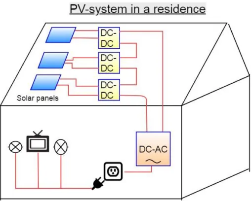
The purpose of the DC-DC converter, in a PV-system, is to deliver right amount of voltage from each PV-module that the inverter requires. Figure 1.1 shows an example of a PV-system on a building, where the DC-DC-converter is placed after each solar panel to regulate the DC-voltage for the inverter. To get the desired power from the PV-modules, the DC-DC converter has maximum power point tracking (MPPT) to control the output power from the DC-DC converter. Following that, an inverter is used to convert power to AC before entering the power grids and the outlet. However, due to switching in the converters, the current is discontinuous and leads to losses and distortion in the system. One of the main problems for a classic inverter conversion is the harmonics distortion where using appropriate switch schemes or cascading the inverters can minimize the distortion.
13 Figure 1.1 Illustration of the PV-system in a building. A DC-DC converter is placed between each photovoltaic module in cascade to regulate a constant voltage to the DC-AC-converter. That converter is regulated by the maximum power point tracker (MPPT) to achieve maximum power from the solar panels.
With the use of the Z-source, the inverter could boost/buck the voltage alone, replacing the DC-DC converter from the PV-system [3].
1.2 Purpose and Motivation
The purpose of the multi-level inverter is to generate a sinusoidal wave that is closer to the fundamental (pure sine wave) signal. Combining the multi-level inverter with the quasi Z-source allows the inverter to boost the voltage before inverting it. This could eliminate the use of a DC-DC converter in the
photovoltaic systems and at the same time lower the harmonic distortion. From an environmental point of view this inverter may reduce the required components and material use, which affect the
environment in a positive way. Our goal is to control and simulate the quasi Z-source topology on three H-bridge inverter modules in cascade for generating a multi-level AC-voltage output. In this thesis we will also implement the quasi Z-source on one H-bridge module to test the boost control, and later cascading three H-bridge modules to test the switching control.
1.3 Problem Statements
The goal of the thesis is to answer these three questions:
• What solution can be used to control the switching for the cascaded multi-level inverter? • How large is the harmonic distortion of the system?
14 When cascading the H-bridge modules together, the AC-output voltage gets a more sinusoidal looking wave. To succeed creating a multi-level AC-output voltage we need to have a switching scheme that controls all three cascaded modules, thus our first question is asked.
The inverter is a nonlinear component, which means that the output voltage will not be a pure sine wave, because of the harmonics. The second question is about the harmonic distortion that could be crucial for sensitive circuits. That is why it is relevant to see how large distortion our simulated and implemented inverter generates.
Adding the quasi-Z source on the H-bridge inverter will need more passive components in the circuit. For our third question we will study the power losses of this new topology.
1.4 Limitations
The simulations of the Quasi Z-source inverter is performed in Simscape by Matlab and later build the quasi Z-source on an existing H-bridge module. The limit is to only implement and evaluate the result. As for evaluating the disturbances of the system our aim is to study the harmonic distortion, which is a common problem when inverting the voltage. Losses are not measured, since it is a difficult task requiring advanced instrumentation. Only calculation of losses is carried out.
Because of the time limitation of ten weeks, we will only focus on the above description, and if time allows us we will also connect a PCB that is designed as a module to simulate a grid-connected PV-system.
15
2. Theory
This chapter describes the following theory that is relevant for this work. First the converter basic for both DC-DC and DC-AC conversion and further on theory for the harmonic study.
2.1 DC-DC Converter
DC-DC converters are one of the most important components that are used in many areas, especially in renewable energy resources as wind power, hydroelectric power and solar energy [4]. There are several types of DC-DC converters used in different areas such as step-down (buck) converter, step-up (boost) converter, step-down/step-up (buck-boost) converter, Cuk converter and full-bridge converter. The basic converter topologies are the step-up and step-down, while the Cuk and buck-boost are a
combination of the basic converters mentioned above, and the full-bridge is derived from the step-down converter [5]. The DC-DC converters are used because of the DC-voltage which is produced by many of the renewable energy resources, which can be transferred from for example the solar energy source to the load. Depending on the load power, the DC-DC converter can be used to match the voltage. If output voltage is higher than the incoming dc voltage, the converter will step up the voltage to match the voltage as mentioned above. Otherwise the DC-DC converter will step down the voltage. Once there is no need to change the voltage, the converter makes the input voltage equal to the output voltage. This is done by controlling converter duty ratio [4].
2.1.1 Control of DC-DC Converters
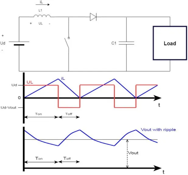
To achieve the desired DC output voltage, the average output voltage must be controlled by controlling on and off durations (Ton and Toff) of the switch, although both input voltage and loads may vary. One or several switches are used to step-up the voltage. Figure 2.1 below explains the conversion in a DC-DC boost converter by using one of several methods called pulse-width modulation (PWM) [5]. By
controlling Ton and Toff durations, the converter generates the average output voltage, Vout which is expressed as [5] 𝑉𝑜𝑢𝑡 =𝑇𝑝𝑒𝑟𝑖𝑜𝑑 𝑇𝑜𝑓𝑓 𝑈𝑑= 𝑈𝑑 1 −𝑇𝑇𝑜𝑛 𝑝𝑒𝑟𝑖𝑜𝑑 .
This is done by regulating the on durations of the switching at a constant frequency, since 𝑇𝑝𝑒𝑟𝑖𝑜𝑑 = 𝑇 𝑜𝑛 + 𝑇𝑜𝑓𝑓, where Tperiod is the switching time period, and Ud is the input voltage. When using the PWM method, the on durations of the switching time is expressed as the duty ratio D, which is varied.
16
Figure 2.1. Illustration of the switch mode DC-DC conversion. The switch time (Ton and Toff) depends on the duty cycle. This will generate a varying voltage, where the output voltage is the average of the signal. Inspired by Ned Mohan, Tore M. Undeland and William P. Robbins [5], figure 7-11 and 7-17.
In order to control the Ton and Toff durations in PWM, a control signal (Switch control signal) is created first by taking the difference between the desired output voltage (Vout) and the actual output voltage and then amplifying it, as shown in figure 2.2. The output control signal (Vc) from the amplifier is then compared with the repetitive waveform (shown as a sawtooth in Figure 2.2.). Once the control signal (V control) is greater than the sawtooth waveform, the switch will be turned on. The constant frequency of the repetitive wave mentioned above creates the switching frequency. The ratio is expressed as 𝐷 = 𝑡𝑜𝑛
𝑇𝑠 = 𝑉𝑐
17 Figure 2.2. Illustration of a pulse-width modulator. Vcontrol is the amplified difference between the desired and the actual signal. The output of the amplifier will be compared with the sawtooth repetitive waveform. Once Vcontrol is larger than the sawtooth waveform, the switch will be closed. From [5], figure 7-3, Copyright © 2003 John Wiley & Sons, Inc.Reprinted by permission of John Wiley & Sons, Inc.
2.2 DC-AC Converter
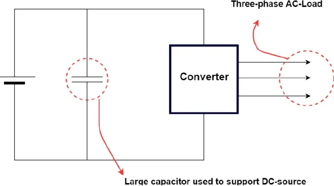
The main circuit in a three-phase voltage source converter is the three-phase bridge, which is normally fed by a DC-source as shown in figure 2.3. Each phase contains two switches which are combined with transistors and anti-parallel diodes to achieve a bi-directional current flow and a uni-directional voltage blocking capability. The purpose of the capacitor located between the dc voltage source and the three-phase bridge is to serve as a voltage source, by feeding the H-bridge during the switch turn on and turn off. This is done to avoid interruptions [3].
If the DC-link voltage is greater than the AC output then the converter works as a buck voltage source inverter for DC-AC conversion. But at the same time, it could work as a boost converter for AC-DC conversion. The switches on each phase are designed to never be on at the same time. Otherwise it will short the power supply and a rush of current occurs, also called a shoot-through [3].
18
Figure 2.3. Illustration of a three-phase voltage source converter with a large capacitor, which works as a voltage source to the main converter circuit (Faris Al-Egli 2018). Inspired by [3], figure 1.
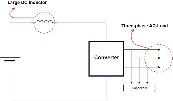
The main circuit in a three-phase current source converter is the three-phase bridge illustrated in figure 2.4. This circuit is normally fed by for example a dc inductor, which in turn is fed by a voltage source (for example a battery). Each phase contains two switches which are combined with for example transistors with a diode in parallel to achieve a bi-directional current flow and a uni-directional voltage blocking capability. Another example is a semiconductor switching device.
The current source converter can also be used as both an inverter (DC-AC) and a rectifier (AC-DC). It will be a boost inverter for DC-AC and a buck rectifier for AC-DC, because the output AC voltage must be greater than the input DC voltage. In order to avoid an open circuit of the dc inductor, two switches need to be on to transfer the current. One switch from the upper level and one from the lower level [3].
19
Figure 2.4. Illustration of the current source converter with a large dc inductor, which works as a current source to the main converter circuit (Faris Al-Egli 2018). Inspired by [3], figure 2.
These two types of converters have some issues. One is that the voltage source converter can only step-down DC-AC, while the source converter can step step-down AC-DC. Another issue is that the main circuit of both converters cannot switch functionality with each other. This means for example that the main circuit of the voltage source cannot be used for the current source converter, or the other way around.
2.3 Single Phase Converter
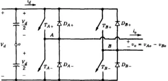
One difference between the three-phase voltage source inverter and a single phase is that single-phase only connects two legs to the load, the structure will represent an inverter as shown in figure 2.5 of the single-phased H-bridge [5].
20
2.3.1 H-Bridge Inverter
Figure 2.5. The schematic illustrates a single phase full-bridge inverter the two legs A (left) and B (right) will connect to each side of the load. TA+ and its diagonal counterpart are closed at the same time to allow the current to flow to one direction, and be reversed when TB+ and TA- takes over. From [5], figure 8-11. Copyright © 2003 John Wiley & Sons, Inc.Reprinted by permission of John Wiley & Sons, Inc.
An H-bridge has two legs (Leg A and B) for driving two directions, where each leg has two switches or transistors that are controlled by the duty cycle. The duty cycle is controlled by a switching schematic that is generated by the pulse-width modulation (PWM). Depending on the switching scheme from the PWM, the output could either look like a square wave or a resemblance of a sine wave.
2.3.2 Pulse Width Modulation
The pulse-width modulation comes in use when generating the gate pulses for the transistors in the converter [5]. It generates the switching signals by comparing a sinusoidal Vref with the switch-frequency triangular waveform Vtri. If Vref is larger than Vtri the top switches (TA+ or TB+) are on and the opposite occur if Vtri is larger. These signals are run by different frequencies as Vtri has the switching frequency fs that decides which frequency the inverter switches are switched. Vref is used to modulate the switch duty ratio and has the desired fundamental frequency, f1 (also called as the modulating frequency).
2.3.3 Control of DC-AC Switching Techniques
There are two well-known switching schemes for the standard H-bridge inverter: the bipolar voltage switching and the unipolar voltage switching.
Bipolar switching is a two-level switching technique that is based on sending two polarity voltage
carriers. By closing one switch with its diagonal counterpart (TA+ with TB- and TB+ with TA- in figure 2.5.) the current will flow to the load. By using this method, the output voltage of each leg sends half of the input voltage Vd as shown in figure 2.6. The output voltage of each leg can be defined as
𝑉𝑜𝐴= + 𝑉𝑑
2 . and 𝑉𝑜𝐵 = − 𝑉𝑑
21 𝑉𝑜= 𝑉𝑜𝐴− 𝑉𝑜𝐵 = 2
𝑉𝑑
2 = 𝑉𝑑.
From this the peak of the fundamental-frequency component, Vo_peak, can be calculated by multiplying the amplitude modulation index with the input voltage [5].
Figure 2.6. Pulse width modulation with a bipolar voltage switching. The comparison between Vref and Vtri sets which switch that should be on. Figure 8-12 from [5]. Copyright © 2003 John Wiley & Sons, Inc.Reprinted by permission of John Wiley & Sons, Inc.
Unipolar switching is a multi-level switching technique that has a third switching stage where the Vtri is
compared with the Vref and –Vref simultaneously. This allows the top switches (TA+ and TB+ in figure 2.6.) or the two lower switches (TA- and TB-) to be closed at the same time, which will set the output voltage to zero. The range of the output voltage travels between +Vd to 0 and 0 to -Vd. This method will yield a softer transition between the output peaks, thanks to the zero stage. The switch frequency can then be increased to the double compared with the bipolar switching frequency and decrease the harmonic distortions [5].
Figure 2.7. The unipolar switching scheme shows a lower voltage jumps from 2Vd at bipolar to only Vd. Figure is from [5], figure 8.15 d). Copyright © 2003 John Wiley & Sons, Inc.Reprinted by permission of John Wiley & Sons, Inc.
22 The switching pulses are done separately for the A and B sides when using unipolar PWM generation. The reference, Vref, is inverted for the B side.
2.4 Harmonics in Waveforms
A common problem with converting the DC-voltage is that the output waveform would not be a pure sinusoidal wave. According to Fourier analysis, a square wave could be described as a sum of many sinusoidal waves, where the amplitude of each sinusoidal wave corresponds N-th order harmonics. Because of the nonlinear components in the inverter, harmonics will appear as sidebands after each multiple of the switching frequency. This could be critical to sensitive components in a circuit. The harmonics could be studied by defining the index frequency modulation ratio =𝑓𝑓𝑠
1
,
where f1 is thefundamental frequency and fs is the switching frequency for the inverter switches. The index amplitude modulation ratio mais also needed to study the harmonics and it is defined by 𝑚𝑎 =𝑉̂𝑉̂𝑟𝑒𝑓
𝑡𝑟𝑖 . The Vref is
the amplitude of the sinusoidal control signal with the frequency f1 and Vtri is the triangular switching amplitude with the frequency fs. In a sinusoidal PWM (SPWM), the linear range is when ma is less than or equal to 1 [5]. It means that the PWM pushes the harmonics to the switching frequency range (high-frequency) and the lower harmonics are smaller. The amplitude of Vtri could be seen as the DC-link voltage of the inverter, and the amplitude of Vref is the desired output signal.
The frequency modulation ratio, mf, is used to define the pulse numbers in the harmonic spectrum, and the amplitude modulation ratio ma is used to control the amplitude of the fundamental-frequency component [5].
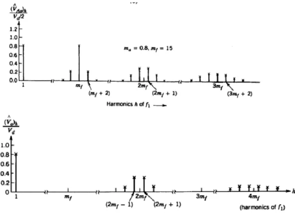
Figure 2.8. A harmonic spectrum for bipolar (left) and unipolar (right) switching in single phase. Note that in the unipolar switching, if mf is even then the odd harmonics will cancel each other out due to the symmetry of 𝑉𝑜= 𝑉𝑜𝐴− 𝑉𝑜𝐵. From [5],
23 The harmonic spectrum for the two switching scheme in figure 2.8 shows a fundamental signal of the 1st
component on the x-axis, as the highest amplitude followed by overtones. The frequency modulation ratio (mf) should be an odd integer for the bipolar PWM, which will cancel out the even harmonics (except its sidebands) so only odd harmonics are shown. But for single-phase unipolar switching scheme, this is not required. The advantage of using the unipolar switching is that it effectively doubles the switching frequency in the spectrum of the output voltage. That means the lowest harmonics will appear as sidebands at twice the switching frequency. When setting mf as even, the harmonics components of the switching-frequency (and sidebands) will cancel each other out as the harmonic component for VoA and the 180 degrees placed VoB is at the same phase. This leads to less ripple compared to the Bipolar switching [5].
In practice the measurement, Total Harmonic Distortion (THD) is used to study the ratio of the harmonic distortion to the fundamental voltage, it is expressed as
𝑇𝐻𝐷 =
√∑ 𝑉𝑛𝑟𝑚𝑠2 2
𝑉𝑓𝑢𝑛𝑑𝑟𝑚𝑠
.
Taking the square root of the sum of all harmonic rms voltage, Vn_rms, and dividing it with the fundamental rms voltage Vfund_rms. Note that voltage is used in the equation above, but current harmonics can also be studied [5].
In a single phase inverter a 2nd harmonic pulsation will appear in the dc-side current. This is not the case for a three phase inverter which only generate high order harmonics at the dc-side related to the switching frequency. The DC-link voltage will then be varying, which is a problem for a sensitive circuit. To avoid the varying voltage at the inverter dc-side, a large capacitor can be added. The dc-side current is defined as
𝐼𝑑 = 𝐼𝑑∗ 𝑐𝑜𝑠(𝑓𝑖) + √2 ∗ 𝑖𝑑2∗ 𝑐𝑜𝑠( 2𝑤 + 𝑓𝑖),
where fi is the AC-side current phase angle and Id is the peak fundamental DC-current and the 2nd harmonic current amplitude id2 can be expressed as 𝑖𝑑2=
𝐼𝑑
24
2.5 Power Losses of the Inverter
Most of the power losses in the inverter occur in the transistors and the diodes. It is due to the switching losses and conduction losses.
2.5.1 Conduction Losses
Conduction losses for one transistor can be defined as: 𝑃𝐶𝑜𝑛𝑑= (
𝑡𝑜𝑛 𝑇𝑠
) ∗ 𝑟𝑑𝑠,𝑜𝑛∗ 𝐼𝑣, 𝑟𝑚𝑠2. Conduction losses occur during the on-interval as 𝑡𝑇𝑜𝑛
𝑠 describes. During that time the output current
𝐼𝑣,𝑟𝑚𝑠 goes through the MOSTFET and generates heat because of the resistance over the device, 𝑟𝑑𝑠,𝑜𝑛. The device resistance value is dependent on the junction temperature and could be estimated from the datasheet.
For an inverter the duty cycle D (also defined as 𝑇𝑇𝑜𝑛
𝑠 ) is varying due to the amplitude modulation ratio
ma
=Vref/Vtri. Although the maximum and the minimum D can be defined as:𝐷𝑚𝑎𝑥= 0.5 + 𝑚𝑎
2 𝑎𝑛𝑑 𝐷𝑚𝑖𝑛= 0.5 − 𝑚𝑎
2 .
On average the duty cycle could is 0.5 when calculation the conduction loss P_cond 𝑃𝑐𝑜𝑛𝑑= 0.5 ∗ 𝑟𝑜𝑛∗ 𝐼_𝑣, 𝑟𝑚𝑠2.
2.5.2 Switching Losses
The semiconductor developer Vishay has published a tutorial about the MOSFET basics and switching delay calculations.From the tutorial, the expression for the switch loss for a MOSFET-device has been derived. During the voltage conversion from DC to AC, there will be some power losses due to the on and off switching of the MOSFETs. The losses are expressed as
𝑃𝑠𝑤 = 0.5 ∗ 𝑉𝑝𝑛∗ 𝐼𝑣𝑟𝑚𝑠∗ 𝑓𝑠∗ (𝑡𝑟𝑖 + 𝑡𝑓𝑣 + 𝑡𝑟𝑣 + 𝑡𝑓𝑖).
The switching losses depend especially on the switching frequency since the voltage Vpn and the current Iv_rms are fixed. The time constants Ton and Toff is the time that it takes for the device to switch from on to off state and vice versa. The turn on time T_on is expressed as 𝑇𝑜𝑛= 𝑡𝑟𝑖+ 𝑡𝑓𝑣, where tri is the rise time of current and tfv is the fall time of the voltage. The turn of time T_off is expressed as 𝑇𝑜𝑓𝑓 = 𝑡𝑟𝑣+ 𝑡𝑓𝑖, where trv is the rise time of the voltage and tfi is the fall time of the current. An approximation of these parameters could be found in the datasheet of the MOSFET device.
It is also possible to determine the switching losses through the device by using a capacitance equivalent of the MOSFET (Cgd and Cgs) and a gate drive that is represented as a voltage source[7], VGG, in series with gate resistance, Rg. The semiconductor manufacturer Vishay has put out a manual about the basic behavior of power MOSFETs. The manual defines the time intervals as: tri = (t_2-t_1), tfv = t_3, trv = t_5 and tfi = t_6 [7].
25 As the time delays are different for each device, there are some values set that can be calculated with the expressions shown in Table 2.1.
Table 2.1. Calculation for the time step for the MOSFET switching 𝑡1 = 𝑅𝑔_𝑜𝑛 ∗ 𝐶𝑖𝑠𝑠∗ 𝑙𝑛 ( 1 1 −𝑉𝑔𝑠(𝑡ℎ𝑉𝐺𝐺(𝑜𝑛)𝑜𝑛) ) 𝐶𝑖𝑠𝑠 @ 𝑉𝑑𝑠 = 25𝑉 𝑡2 = 𝑅𝑔𝑜𝑛∗ 𝐶𝑖𝑠𝑠∗ 𝑙𝑛 ( 1 1 − 𝑉𝐺𝑃 𝑉𝐺𝐺(𝑜𝑛) ) 𝐶𝑖𝑠𝑠 @ 𝑉𝑑𝑠 = 25𝑉 𝑡3 = 𝑅𝑔𝑜𝑛∗ 𝐶𝑟𝑠𝑠∗ ( 𝑉𝑑𝑠 𝑉𝐺𝐺(𝑜𝑛)− 𝑉𝐺𝑃 ) 𝐶𝑟𝑠𝑠 @ 𝑉𝑑𝑠 = 2.5𝑉 𝑡5 = 𝑅𝑔𝑜𝑓𝑓 ∗ 𝐶𝑟𝑠𝑠 ∗ ( 𝑉𝑑𝑠 𝑉𝐺𝑃 ) 𝐶_𝑟𝑠𝑠 @ 𝑉𝑑𝑠 = 2.5𝑉 𝑡6 = 𝑅𝑔𝑜𝑓𝑓 ∗ 𝐶𝑖𝑠𝑠∗ 𝑙𝑛 ( 𝑉𝐺𝑃 𝑉𝑔𝑠(𝑡ℎ𝑜𝑓𝑓) ) 𝐶𝑖𝑠𝑠 @ 𝑉𝑑𝑠 = 0𝑉
The input capacitance (Ciss) and the reverse transfer capacitance (Crss) can be found in the datasheet of the device. The VGP stands for the miller plateau voltage of Vgs and the Vgs(th) is the gate threshold voltage for either turn-on or turn-off [7].
The switching loss can then be expressed as
𝑃𝑠𝑤 = 0.5 ∗ 𝑉𝑑∗ 𝐼𝑜∗ 𝑓𝑠∗ (𝑡𝑟𝑖 + 𝑡𝑓𝑣 + 𝑡𝑟𝑣 + 𝑡𝑓𝑖),
for each device. The current I_o can, for simplicity, be expressed as the average from I_v,rms 𝐼𝑜= (2 ∗√2𝜋) ∗ 𝐼𝑣,𝑟𝑚𝑠 .
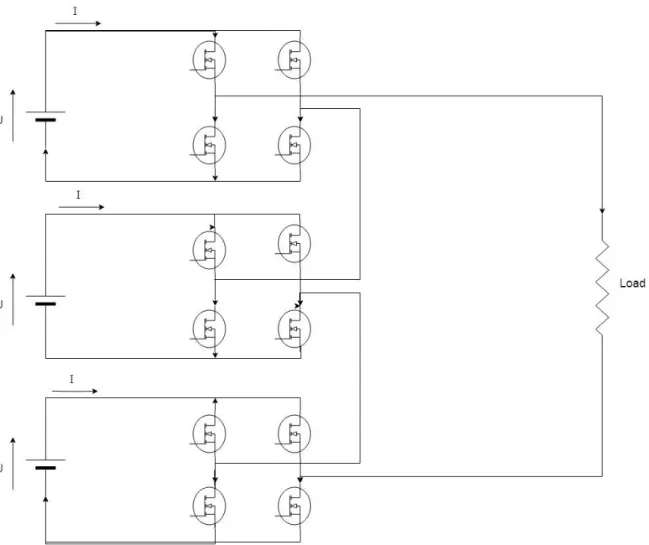
2.6 Cascaded Multi-Level H-Bridge
The multi-level inverters (MLIs) have been widely used in many areas for example in flexible alternating current transmission systems, high voltage direct current transmission, photovoltaic system and other medium and high voltage applications. There are three well known MLI topologies such as neutral point clamped, flying capacitor and the cascaded H-bridge (CHB). The CHB is the most frequently used
topology, especially at higher voltage levels (> 10kV). One advantage with this topology is that with low voltage power semiconductor in the H-bridge components, the combination of many H-bridges can achieve a high output voltage that can get close to a sinusoidal shape. By adding more H-bridges in cascade, the system will generate a more shaped sinusoidal output. It will also increase the total output power due to the summation of all the H-bridge outputs. The other advantages are the decreasing of harmonics distortion and decreasing the switching losses as each H-bridge can use lower switching frequency compared to one H-bridge module [8].
26 Figure 2.9. A simplified sketch of three cascaded H-bridge inverter with the dc-input voltage Vd and Ac-output voltage Vo. Each switch is representing a MOSFET [Hassan Moumin 2018]. Inspired by [1], figure 1.
The cascaded H-bridge is structured by connecting the output of the H-bridge in cascade. Each H-bridge has a separate input dc-voltage. This could be a drawback for systems with only one dc-source, although it is a good reason for using it in PV-systems, due to many PV modules. Some remarks on using the cascaded multi-level inverter is that the PWM phase shift PHs is determined by the number, N, of H-bridges, 𝑃𝐻𝑠 = 360
𝑁
. to distribute voltage phase over 360 degrees. That will give out a total output
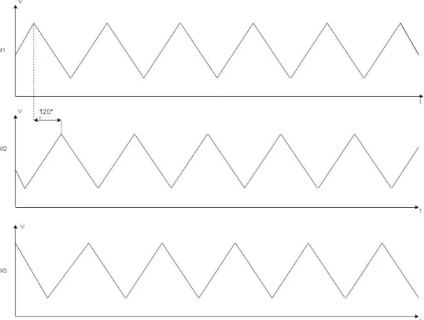
voltage that looks more like a sinusoidal wave [1].27 Figure 2.10. The graph illustrates Vtri signals of each inverter module (M1, M2 and M3). Due to having three modules the phase should be shifted by 120 degrees [Hassan Moumin 2018]. Inspired by [1], figure 4.
2.7 Z-Source Converter
The common issues mentioned earlier under the first section for inverters and converters can be solved by using an impedance source power converter, also called a Z-source converter. This type of converter can control all types of methods, DC-AC, AC-DC, AC-AC and DC-DC.
A Z-source converter has a unique structure. As illustrated by figure 2.12 below, a Z-source converter is a combination of the voltage and current source converter, where both a capacitor and an inductor are used between the DC voltage source and the converter’s main circuit. This will provide a wide range of input voltage that the traditional voltage and current source converter cannot obtain.
The topology includes two inductors and two capacitors that are connected in an X shape to provide an impedance network which gives a different power conversion. This converter can be connected to either a DC voltage source or a current source, where different components can be used as DC voltage source, such as a battery, an inductor or a thyristor converter etc. There is a possibility to use a diode in series with the voltage source to block the reverse flow of current [3], [9].
28 Figure 2.11. Illustration of the Z-source converter. This topology has an x-shaped impedance network between the source and the converter. This will allow two switches connecting on the same leg at the same time, which in turn will give a shoot-through state (Faris Al-Egli 2018). Inspired by [3], figure 3.
The Z-source can be connected with two types of inverters, for example a half-bridge or an H-bridge inverter. The H-bridge inverter is operated as mentioned in the section 2.3, where it has seven different states when connecting to single phase loads. However, unlike a traditional converter the Z-Source inverter has the ability to allow both switches be closed on the same leg, creating short-circuit. This is needed to have the shoot-through state which in turn will charge the inductors and then later step-up the AC output voltage magnitude during the non-shoot-through state.
The single-phase Z-source inverter has seven switching states. Two of them are the active stage and two are null states as table 2.2 shows. The rest are shoot-through states. During the shoot-through the output voltage will be kept at zero, which in turn is like a null state. As described in the section about multi-level switching, the null states are used to provide a smoother transition between the output voltage peaks, and this will also lower the harmonic distortion. During a switching cycle T, the null states occur before and after an active state. With ZSI the shoot-through states should occur during null intervals, leaving the active state untouched. An example from a previous study shows that the shoot-through interval should occur half of the null interval before and after the active state [10].
Figure 2.12. Illustration of the shoot through state. When two switches are connected on the same leg at the same time, which in turn will charge the components (Faris Al-Egli 2018). Inspired by [9] figure 4.
29 Table 2.2. The different switching states depending on the coordination of the transistors S1-S4. ‘1’ stands for conducting and ‘0’ for open switch (not conducting).
State S1 S2 S3 S4 Active, positive 1 0 0 1 Active, negative 0 1 1 0 Null, 00 0 1 0 1 Null, 11 1 0 1 0 Shoot-Through 1 1 S3 !S3 Shoot-Through S1 !S1 1 1 Shoot-Through 1 1 1 1
The transistors S1-S4 represent the following switches from figure 2.5 in section 2.3.1: S1 => TA+, S2 => TA-, S3 => TB+ and S4 => TB-.
2.8 Quasi Z-Source
One of the most studied quasi Zsource- inverter, QZSI, topologies is the voltage-fed continuous input current [11a]. The main perks of using the voltage-fed continuous input current quasi Z-source inverter is that the QZSI can use fuel cells, PV-modules or batteries as a voltage source. The structure difference between the Z-source and quasi Z-source inverter is as shown in figure 2.14. The new connections are the components where the inductors are connected to the same polarity side of the source. There are two features in the QZSI that decrease the system cost and provide better efficiency. One feature is that it uses less components, compared to having a separate DCDC converter. -For example there are no other switches except in the H-bridge and it does not need a control signal [2].
30 The big difference between a QZSI and a traditional VSI is that the QZSI can both make the voltage inversion and step-up at the same time, thanks to the impedance network. The switching stages are the same as a ZSI (table 2.2). During shoot-through (Fig 2.14 (2)), the two inductors are charged in parallel, and inductor L1 works together with the capacitor C1 and L2 with C2. The shoot-through is performed during a null state when the inverter output is zero. During the non-shootthrough state (Figure 2.14 (1)), the DC-link voltage to the H-bridge, Vpn, is built up as the sum of the two capacitor voltages and is defined as Vpn= Vc1 + Vc2 [2].
Figure 2.15. The behavior during 1) non-shoot-through and 2) shoot-through state of the quasi-Z-source
In the non-shoot-through state, the capacitors are now providing DC-link voltage Vpn via the H-bridge to load. Then H-bridge switches to provide an active or null state. In the active state the AC current flows to the load and sends out the collected voltage Vpn. At the null state the AC-output will be zero and occurs when either the top or bottom transistors are on, as explained for the unipolar switching. The diode is used to block the reversed current to the source.
31 The voltage boost in the QZSI, defined as the ratio between the DC-link voltage Vpn and the input voltage, Vin, is dependent on the shoot-through cycle and the modulation index. The estimated voltage boost factor B is
𝐵 =𝑉𝑝𝑛 𝑉𝑖𝑛
= 1
1 − 2 ∗ 𝐷𝑠,
with shoot-through duty cycle Ds defined as the duration of shoot-through intervals during each switching cycle. The shoot-through time is limited related by the duration of null state, resulting in a maximum of Ds given by:
𝐷𝑠 ≤ 1 − 𝑚𝑎,
where ma is the modulation index. In a linear ranged SPWM with the amplitude of Vtri equal to 1, the shoot-through time T0 is at its maximum when Ds is equal to 1-ma [2]. This defines the maximum boost factor B for the system. After boosting the voltage Vpn is then inverted through the H-bridge, giving out an output voltage peak 𝑈̂𝑎𝑐 = 𝑚𝑎 ∗ 𝑉𝑝𝑛. The voltage gain for the inverter, the ratio between peak AC-output and DC-input voltage, can be estimated as Gain = ma*B. The graph below shows a maximum gain that can be reached for each modulation index.
Figure 2.16. Illustration of gain VS modulation index, ma.
For an ideal case the input power Pin should be equal as the output power Po. Then the current Iin can be estimated to be:
𝐼𝑖𝑛 =
𝑉𝑖𝑛 𝑃𝑜=
𝑉𝑖𝑛 (𝑈𝑎𝑐𝑅𝐿2 ) ,32 When inverting in single phase the 2nd harmonic (doubled fundamental frequency) is always a problem because of the AC-ripple [6]. The component values for the QZSI can be selected to minimize current and voltage ripple as presented in [6]. The minimum size of the inductor is then defined as
𝐿1 = 𝐿2 ≥
𝑉𝑝𝑛𝑟𝑖𝑝𝑝𝑙𝑒∗ 𝑉𝑖𝑛∗ (1 − 2 ∗ 𝐷𝑠) 2 ∗ 𝑤 ∗ 𝐼𝑖𝑛𝑟𝑖𝑝𝑝𝑙𝑒∗ 𝑚𝑎 ∗ 𝐼𝑜𝑢𝑡
,
where Vpn_ripple and Iin_ripple is the allowed ripple at the DC-link voltage and input current. The ripple is expressed as 𝑉𝑝𝑛𝑟𝑖𝑝𝑝𝑙𝑒=𝑉̂𝑝𝑛
𝑉𝑝𝑛. 𝑉̂𝑝𝑛 is the ripple voltage for the DC-link voltage. The inductor currents IL1 and IL2 are equal to the input current. The values for the capacitor can be expressed through the same variables to lower the 2nd harmonic influence and the derived capacitor values are
𝐶1 = 𝐶2 ≥1−𝐼𝑖𝑛𝑟𝑖𝑝𝑝𝑙𝑒∗𝐼𝑜𝑢𝑡∗(1−2∗𝐷𝑠)∗𝑚𝑎 2∗𝑤∗𝑉𝑝𝑛𝑟𝑖𝑝𝑝𝑙𝑒∗𝑉𝑖𝑛 .
2.9 Multi-Level Inverter Circuit
For this work the Multi-level inverter (described in section 2.8) will be a full-bridge (H-bridge) inverter module from Linköping University that is connected in cascade. This H-bridge has been used in electrical engineering courses and is designed by Tomas Uno Jonsson. To set-up the multi-level conversion three modules will be cascaded according to figure 2.9 in section 2.8.
2.9.1 Overview of the Full-Bridge Inverter
The inverter module could be divided into three blocks: Gate pulse logic (Gate pulse interlocking), Gate drives and the FB-Inverter core that contains MOSFETs and diodes.
There are two different voltage supplies for the components on the board. The board needs 5V supply for the digital circuit and 15V for the gate drivers. The board has 8 measurement signals that can be used to communicate with the Elvis board. For this project 3 signals have been used for measuring the output voltage for S1-S2 leg (U_op), output voltage for S3-S4 leg (U_on) and the DC voltage (Vpn). All the measurements are viewed in Labview, which also sends the control signals for the gate pulses. The detailed view of the module can be found in appendix 2.4.
2.9.2 Gate Pulse Interlocking
The purpose of the gate pulse interlocking is to avoid short-circuit in the system. The first AND-gate logic makes sure that the transistors on the same leg would not close at the same time. The second AND-gate compare with the deblock signal that is a physical switch for the module. The deblock must be on to start the gate pulses.
33 Figure 2.17. Illustration of non-overlapping gates used in the system. Reproduced with permission of Tomas Uno Jonsson.
2.9.3 Gate Driver
At the gate drivers, the PWM gate pulses are converted to the final gate-source voltage. The figure below shows that the gate drive block uses optical sensors to trigger the pulse signals. This allows a proper turn on and turn off. Each side has their connected ground which provides isolation besides the actual gate current driving.
Figure 2.18. A schematic that illustrates one of the gate drivers in the H-bridge module. Reproduced with permission from Tomas Uno Jonsson.
2.9.4 Full-Bridge Inverter Core
The full bridge inverter contains four power MOSFETs where each transistor has a power diode. The switching signals for the transistor gates are sent from the gate drivers, which in turn controls the output signal depending on the switching signal. The output signal is generated due to the MOSFET different states, such as shoot through state, active state and null state.
34
Figure 2.19. Schematic of the FB-inverter core used in the system. Reproduced with permission of Tomas Uno Jonsson.
35
3. Method
The goal of this work is to set up a QZSI-module that can step up from 5V DC input to 15V AC output. In the beginning the QZSI is designed to be controlled as one module, before we connect it with two more modules in cascade. Once the module succeeds the goal, the modules should then be cascaded to set a total output voltage of 45V AC. Our approach to solve the problem statements will be described from the design of the topology to studying the result for the QZS cascaded H-bridge multi-level inverter.
3.1 Control and Design
To generate gate-pulses for controlling the H-bridge switching, a gate driver block was made to deliver four pulses (G1-G4). The gate-driver has three inputs: Control signal (Vref), Switching signal (Vtri) and an amplitude offset. These inputs are used for the pulse width modulation (PWM). The construction of the PWM is redesigned according to a unipolar switching scheme. The used values for the PWM are switching frequency fs= 2.5kHz, (mf=50)
modulating frequency f1= 50Hz, modulation index ma= 0.6,
where the triangular wave, Vtri, peaks between +1 V and –1 V. To allow shoot-through, the Vref signals for the switches at the same leg shall have an amplitude offset closer to the Vtri peaks. The offset will shorter the off-interval for one of the switches and lead to both conducting simultaneously
(shootthrough). The higher the offset is, the longer the shoot-through time will be. When Vref is at the positive interval the amplitude of the top switches (TA+ and TB+) is raised with the offset to set the shoot-through range. During the negative interval the bottom switches are lowered for the negative output shoot-through interval.
Figure 3.1. Inside the gate driver block in Simulink. The inputs are the control signal (Vref), switching signal (Vtri) and the amplitude offset (Amp offset). This block will generate the gate pulses for the H-bridge.
The method to have an offset between the Vref signals has been used in the original design to set a blanking time to avoid shoot-through. The goal with the simulation is to control the MOSFETs with the pulse-width modulation that provides enough shoot-through for our reference boost factor.
36 The shoot-through duty-cycle Ds is the amplitude offset for the system. The offset between the two Vref signals is setting up a switching delay as one of them will reach the Vtri waveform later than the other. That delay will allow both switches to be on at the same time for a short interval, t0 in figure 3.2. The way to obtain the maximum boost in the system is by having the control signal Vref at the maximum point of the triangular signal Vtri. The fixed Vtri amplitude value is 1. The sum of modulation index, ma, and duty cycle cannot exceed the maximum point. Which means that the duty-cycle limit is equal to
1-ma. However, to prevent Vref to exceed above the Vtri peak, a logic gate function for limitation was
built as figure 3.2 shows. The duty cycle is calculated in a Matlab function block that derives the boost factor by dividing the desired gain with the modulation index. The boost factor will then be used to derive the duty cycle.
37 Figure 3.3. Logic gates used to avoid Vref being raised above Vtri, a maximum-boost logic scheme was made to control the input signal.
To set up the H-bridge inverter, four MOSFETs blocks in Simulink are connected as an H-bridge topology.
Figure 3.4. An illustration of the H-bridge that was used for this project. It is built up by four MOSFETs that are controlled by the gate driver to generate a desired AC voltage to the load.
The system is set to have resistive load with a power output of 3W. When having a 15V peak AC output Uac, the load resistance can be estimated as
𝑅𝐿 =( 𝑈𝑎𝑐 √2) 2 𝑃 = 152 2∗3= ~38Ω, where RL is the load resistance for one QZSI-module.
The component values for QZSI were calculated by previously mentioned in the theory 2.9, which was implemented in Matlab to be able to achieve voltage boosting. The structure of the QZSI was made in
38 Simscape by Matlab as shown in figure 3.4 below. For an ideal case, the inductor resistance was set to 0.1 Ohm and the forward voltage of the diode was set to 0.7V. Following that the calculated values for the inductors L1=L2=6.8mH and the capacitors C1=C2=750uF.
Figure 3.5. Illustration of the Quasi Z-source inverter.
The goal for this module is to use 5V as DC input and later step up the voltage with a boost factor =1−2∗𝐷1 . After the voltage boost, the H-bridge will invert the voltage to 15V AC. With the simulated output voltage, the harmonics are going to be measured by using the FFT-analysis tool in the powergui. Our first approach to initiate a multi-level unipolar SPWM is to phase-shift triangular signal Vtri with 120° between each H-bridge module as shown in section 2.8. To cascade the modules, the positive output from the first module is connected with the negative port of the second module. The result should give an output voltage with less THD than without cascading it as it is mentioned in previous studies [1].
3.2 Implementation and Study
The reconstruction of the H-bridge includes several reconnections of different components. The first problem to solve is the design of the Non-Overlapping-gates as shown in figure 3.6a), where the not-gates hinder the quasi Z-source from operating in shoot-through state. The grounding of the
Opto-coupler input, as shown in figure 3.6.b), is not allowed to share the same ground as the
gate-drivers. Otherwise problems with the potential voltage will occur in the cascaded H-bridge multi-level inverter.
The approach to allow the shoot-through is to remove the first AND-gates in the Non-overlapping-gate and reconnect the gate pulse inputs to the second AND-gate to let the signal through. This will make sure the H-bridge can be short-circuited. To solve the varying potential at the optical gate drivers grounding, the first approach is to see if an external cable can be used to ground the optical gate
39 sensors. Another approach is to add an external optical gate sensor that will trigger the optical sensor on the module.
The MOSFETs used in the H-bridge module is IRF540 from Vishay. To calculate the power losses from the inverter, we will go by its datasheet and our simulated power sources.
The values for our loss calculation are: • Ton = 728ns,
• Toff = 56ns, • Fs = 2500Hz, • r_on = 0.077ohm, • duty_cycle = ma,
and Vpn and I_out (Iv_rms) will be measured from the simulation.
Calculations of power and conduction losses were made in Excel. Formulas used for these calculation are mentioned in section 2.5. For the power loss over the inductors, the approach is to measure the internal resistance of the component and the input current, Iin.
The QZSI will be built up at the input of the module and connected with one H-bridge. This will give an opportunity to verify the Matlab simulations and study the harmonics distortion in the output voltage by using total harmonic distortion (THD) in Labview. The THD will give out the harmonics in % and will be the result. Continuing later, two more H-bridges shall be connected in cascade without the quasi Z-source. This will also give an opportunity to study the changes of the harmonic distortion and the output voltage.
Figure 3.6. A photo of the H-bridge PCB, used in courses as “Power electronics” at Linköping University. The circles have marked the NonOverlapping-gates a) and the optical gate-drivers b). Photo taken by Hassan Moumin.
40
3.2.1 Construction on ELVIS Platform
Figure 3.4 below presents our final construction of one QZSI module, where the A marking shows a DC voltage source, which generated the desired DC current and voltage to the QZSI.
The QZSI was build up on an ELVIS platform which was connected to Labview via a computer. Because of time limitations we had to use existing components and therefore we could not reach the calculated values. The inductors (L1 and L2 at each side of L in figure 3.6) became 6mH instead of 6.8mH and the capacitors (C1 & C2) became 990uF instead of 750uF. The diode had a forward voltage of 0.7V [13a]. The H-bridge is also connected to the ELVIS platform via signal wires that is controlled from Labview. The variable load unit was set as 34ohm. The Labview schematic was built up as the PWM schematic from Simscape with the duty-cycle calculation for the offset. The schematic is presented in Appendix 9.1.
Figure 3.7. The whole QZSI-module set. A) the voltage source, B) the Quasi Z-source with L, C1 and C2 as the components, C) the H-bridge and D) the variable load unit.
41
4. Result
This section shows our result for this work. First how we designed the shoot-through control. One QZSI was first implemented in Simulink to provide the correct output signal and later two more. The resulted measurement and calculations will be presented for an ideal and non-ideal simulation, and for the implementation.
4.1 Pulse Width Modulation Simulation
To set up the H-bridge inverter, we took four MOSFETs in Simulink and connected them in an H-bridge topology. To generate the gate-pulses (G1-G4), a gate driver block was made to deliver the four pulses. Inside the gate driver block, the control signal Vref is modified for each gate pulse to generate a unipolar switching scheme with an offset. The amplitude offset is decided by the duty cycle and as the larger 𝐷𝑠 is, the longer shoot-through interval the QZSI has. The offset is raising the top gates signal when Vref is positive and lowers the bottom gate signal when negative (figure 4.2). This is shortening the gate pulse “off”-interval to allow its neighbor gate on the same leg to be on at the same time.
Figure 4.1. The plot of the four gate signals. The shoot-through occurs when G1 and G2, G3 and G4 or all four gates are active at the same time.
During the shoot-through the inductor current will charge up until the active stage. At the active stage the capacitor stores the energy from the inductor and will send out the DC-link output voltage together with the other capacitor.
42 Figure 4.2. A plot of the behavior of the capacitor voltage and inductor current during shoot-through.
43
4.2 Confirmation of Simulation in an Ideal Case
In an ideal case, the passive component resistance was chosen to be 0.1 Ohm, leading to a low voltage drop across the system. The reason for this is to give out a closer result to our specification: inverting a 5V DC input to a 15V AC output.
4.2.1 Simulation Results from the Quasi Z-Source
The DC-link input voltage to the H-bridge Vpn is estimated to be 18V, meaning that the system has a boost factor at 3.6. The sum of the voltages over the capacitors C1 and C2 is the Vpn value as the figure below shows our simulated Vpn with the capacitor voltages VC1 and VC2.
Figure 4.4 Illustration of the capacitor voltages Vc1 and Vc2 during steady state. The sum of the voltages is the total DC-link voltage, Vpn, to H-bridge.
The input current for the system Iin was estimated to be 0.95A for the ideal case. The current Ipn is measured to be 0.86A to the H-bridge.
44 Figure 4.5. The current measurement of the Ipn and Iin is shown to be 0.86A and 0.95A.
4.2.2 Input and Output Signal
With an input voltage of 5V and a current of 0.9A combined with a boost factor of 3.6 and an output power of 3W, the fundamental output voltage peak 𝑈̂𝑎𝑐 is measured to be 12V for this ideal case. That means the shown voltage across the 38 Ohm load is a little above 8V and load current of 0.2A. The figure X below shows the measured output of the one module QZSI.
45
4.2.3 Simulation of the Cascaded QZSI in an Ideal Case
The multilevel inverter was connected to a 114 Ohm load (38 Ohm x 3) and the fundamental output voltage peak at 50Hz is measured to be 34V. The conversion of the cascaded modules is a three level that is shown in the figure 4.6.
Figure 4.7a. The output voltage peak from the cascaded QZSI is measured to be 34V.
Figure 4.7b. The plotted graphs show that the cascaded QZSI has an output current at 0.2A AC.
4.3 Confirmation of Simulation in a Non-Ideal Case
Because the ideal case is not compatible with the practical measurement, the inductor and diode now have internal resistance that will lead to a voltage drop at large currents. The component values for the QZSI were also comprised to using an inductor size of 6mH and capacitors at 990uF. To change the minimum inductance size from the size-calculation, the resistive output load was lowered to 34 Ohm. When using the Impedance analyzer in Labview, the internal resistance of the used inductor was measured to 2.9 Ohm (excluding the resistance of measurement leads of 0.65 Ohm).
46 Figure 4.8. A measured internal resistance for one of the inductors that will be used in the circuit. This was done through impedance analyzer in Labview.
4.3.1 Vpn and VC1 & VC2
At the non-ideal state, the DC-link voltage was measured to 7V. The boost factor is at 1.4. Figure 4.8 shows the plot of capacitor voltages with the Vpn.
47
4.3.2 Simulation of the Iin and Ipn
The measurement of the Iin and Ipn for the non-ideal case gave Iin=0.43A and Ipn=0.9A.
Figure 4.10. The measured input current Iin and DC-link current Ipn during steady state.
4.3.3 In and Output Simulation
The measured output voltage peak at 50Hz was at 5.1V with a load current at 0.11A. .
48
4.3.4 Harmonics
During steady state, after 0.3 s, the estimated THD for the output voltage is approximately 105%, as shown in the figure below. The red signal is the steady-state interval considered for the FFT. The fundamental voltage is also presented from the FFT and shows a delivered output voltage of 4.67V.
Figure 4.12. The THD of the non-ideal voltage output is measured through the FFT analysis tool in Simulink.
4.3.5 Losses
The voltage drops over the inductors can be calculated as 𝑉𝑙𝑜𝑠𝑠= 2 ∗ (𝑅𝐼𝑛𝑑∗ 𝐼𝑖𝑛) + 𝑉𝐷 , with
Inductor resistance 𝑅𝑖𝑛𝑑=2.9 Ohm, Input current Iin=0.43A, Diode forward voltage 𝑉𝐷=0.7V, leading to a voltage drop of one QZS-module at 3.2V and a power loss over the inductors to calculated as
𝑃𝑖𝑛𝑑𝑙𝑜𝑠𝑠= 𝑅𝑖𝑛𝑑∗ 𝐼𝑖𝑛2 ∗ 2 = 2.9 ∗ 0.432∗ 2 = 1.07𝑊.
According to the simulations in Matlab and the calculations in Excel, the conduction losses 𝑃𝑐𝑜𝑛𝑑 for one MOSFET became approximately 0.56mW by using the parameters in table 4.1 below, and the switching losses for one switch became 1.94mW, according to table 4.2.
49 Table 4.1. Conduction loss calculation for one MOSFET.
Conduction loss calculation
Total rms current Iv,rms (A) 0.11
resistance over the device r_on (Ohm) 0.077
average duty cycle D_avg 0.6
Conduction losses P_Cond (mW/Switch) 0.559
Table 4.2. Switch loss calculation for one MOSFET.
Switching loss calculation
Input voltage to converter Vpn (V) 18
total rms current Iv_rms (A) 0.11
Switching frequency fs (Hz) 2500
On durations (switching time) T_on (s) 728e-9 Off durations (Switching time) T_off (s) 56e-9 Actual current during conduction I_o (A) 0.099
Switch losses Psw (mW/Switch) 1.94
The total loss for one H-bridge inverter is the sum of switching and conduction losses, which is
estimated to 10mW. Total loss for one QZSI (power loss for the inductors and H-bridge) is estimated as 1.08W.
4.3.6 Cascaded Quasi Z-Source Inverter
In order to increase the output signal, two extra modules were added. In the following a presentation of total output signal is presented together with both the THD and the losses.
As the previous studies have shown, the output voltage from each H-bridge module should be added when having the modules in cascade [1].The non-ideal simulation of the three cascaded H-bridge inverters gave a fundamental output voltage peak of 20V.
50 Figure 4.13 A. The output voltage of the three cascaded QZSI. The fundamental output voltage peak is 9V.
Figure 4.13 B. The output current of the three cascaded QZSI. The load current is 0.18A.
The measured harmonics for the cascaded quasi Z-source inverter were estimated to 32.97% at steady state. The fundamental (50Hz) output voltage is measured as 19.82V.
51 The total losses for all three cascaded modules are as previously mentioned the sum of the switching and conduction losses for each module, which is approximated to 11.4mW.
4.4 Confirmation of Implementation
For the implementation the one QZSI module was built on an Elvis board and measured through Labview. The control signals in Labview were designed to allow shoot-through as the one on Simscape. Figure below show a plot for the PWM and gate-pulses for the system.
52 Figure 4.16. The gate-pulses allows shoot-through as the Simscape plot.
A control panel is used to gather all the information for the implementation measurement. The result showed:
Fundamental output voltage peak (Uop-Uon) at 3.24V, DC-link voltage (Upn) as 7V,
and an output current peak (Iv) at 0.41A. The harmonic measurement THD is approximately 58% for the system.
53 Figure 4.17. The control panel in Labview. The fundamental output voltage peak (Uop-Uon) is measured to be 3.24V.
54
5. Discussion
The discussion will cover three parts of this work: the result, our method and possible upcoming work for this subject.
5.1 Result
The big difference between the simulation and the implementation was the output signal from QZSI, where the internal resistance of the inductors was one of the main reasons. The output signal was approximately 12V from each module during the ideal simulation stage but got much smaller during the non-ideal and implementation stages due to voltage drop across the inductors and the diode. Another reason was the disturbance on the measurement signals created by the different connections. There are a few solutions that could be implemented to improve the output signal. As presented in Figure 3.6 in section 3.2, connections between the H-bridge and QZSI could be developed by for example having better connection for each component and between the elements. Another solution is to have better connection when soldering the signal to the correct input in the H-bridge.
5.1.1 Simulation Ideal Case vs Our Expectations
The goal was to boost a 5V DC input voltage to a 15V AC output voltage. According to our calculations the boost factor should be 5 times the input voltage and the gain 3. In the simulation of the ideal case, our output voltage peak reached 12V with a boost factor of 3.6 times. This means that the output voltage is 20% less than we expected. The reason for this can be the voltage drop through the diode, which had a forward voltage of 0.7V in the ideal case and a resistance of 0.07 Ohm [12]. Other reasons can be the losses from the MOSFETs.
5.1.2 Simulation Ideal Case vs Non-Ideal Case
When comparing the ideal case with the non-ideal case it shows a large voltage loss in the system (58% less compared to the ideal case). The inductor in the non-ideal case has a large internal resistance that affected the boosted voltage Vpn. Vpn had a value of 7V, meaning that the boost factor was 1.4. The voltage loss can be calculated as 𝑉𝑙𝑜𝑠𝑠 = 𝑅𝐼𝑛𝑑∗ 𝐼𝑖𝑛+ 𝑉𝐷 . The voltage after the losses V can be calculated to 𝑉 = 𝑉𝑖𝑛 − 𝑉𝑙𝑜𝑠𝑠 = 5 − (2.9 ∗ 2) ∗ 0.43 − 0.7 = 1.8V, where the resistance in the inductors are 2.9 ohm each and the voltage across the diode is approximately 0.7V. The DC-link voltage was estimated to 𝑉𝑝𝑛 = 5 ∗ 1.8 = 9𝑉. The output voltage was measured to 5.1V. If we compare our calculated Vpn according to 𝑈𝑎𝑐 = 𝑚𝑎 ∗ 𝑉𝑝𝑛= 9 ∗ 0.6 = 5.42𝑉.
5.1.3 Simulation Non-Ideal Case vs Implementation
By comparing the non-ideal case with the implementation the output voltage in the Labview
measurement was 36% less than expected (5.1V vs 3.24V). This has several explanations such as the cable resistance that we could not have taken into account in the simulation because of time limitation. We have noticed some disturbances in measurement that are created by the signal cable between the ELVIS platform and the H-bridge that could be a reason. Other problems that could have increased the disturbances are the rewired gate pulse signals at the non-overlapping logic gates. One reason could be power losses in the cables between the components in QZSI.