Master Thesis CDT504
Electronic Design Optimization of
Vibration Monitor Instrument
2012 November 22
Fredrik Lindh
Mälardalen University flh07001@student.mdh.seThomas Otnes
Mälardalen University tos07001@student.mdh.seJessica Wennerström
Mälardalen University jwm07002@student.mdh.seAddiva Consulting
Kopparbergsvägen 8 722 13 VästeråsSupervisor: Björn Lindström
bjorn.lindstrom@addiva.seMälardalen University
Innovation, design and engineeringBox 883
721 23 Västerås, Sweden +46-21-10 13 00
Supervisor: Mikael Ekström
mikael.ekstrom@mdh.seExaminer: Mats Björkman
Abstract
Vibrations in machines increase friction on moving parts which cause chafing that will tear down the fabric of the machine components when given time, thus monitoring and analysis of machine vibrations are important for preventive maintenance. Vibration analysis utilizes time domain as well as frequency domain analysis for which there have been analog solutions for quite some time. This work has been about moving a predominantly analog mixed signal system onto an FPGA and making it mostly digital. Vibration analysis on an FPGA have its own challenges and benefits compared to other methods. The inherent parallelism of the FPGA makes it suitable for high performance signal analysis. This report shows through two proof-of-concept solutions that the translation of a predominantly analog system is viable, economic and can deliver improved performance. The two solutions have utilized two different units from Xilinx, the Spartan-6 FPGA and the Zynq-7000 system on chip FPGA. The solution implemented on Spartan-6 produces a result in 9.32 ms and the other implementation based on Zynq-7000 produces a result in 9.39 ms, which is more than a 10-fold increase in performance of the current system. The results obtained show that both solutions can perform the calculations for the proof of concept within 20% of the allotted time. Costs of both solutions as well as other qualities of each solution are presented in this paper.
Table of Contents
1 Background...1
1.1 Abbreviations...2
2 Relevant theory...3
2.1 Vibration Measurement and Analysis...3
2.2 Sampling and aliasing...3
2.3 ADC...4
2.4 Fast Fourier Transform...4
2.5 Filters...5 2.6 FPGA...5 2.7 SoC...5 3 Related Work...6 4 Problem Formulation...6 5 Analysis of Problem...7 5.1 Measurement module...7 5.1.1 Overview...7 5.1.2 Filter Block...7 5.1.3 ADC Block...8 5.1.4 DSP Block...9
5.1.5 I/O configuration and control (IOCC) block...9
5.1.6 EtherCAT block...10
5.2 System requirements (Measurement module)...10
5.3 Component cost (Measurement module)...10
5.4 CPU-module...11 6 Method...12 7 Research...13 7.1 Filter...13 7.2 ADC...13 7.3 DSP...13 7.3.1 FFT...13 7.4 EtherCAT...13
7.5 FPGA / Soc FPGA...13
8 Research Results...14 8.1 Analog Filters...14 8.2 Digital Filters...14 8.2.1 FIR description...14 8.2.2 FIR Compilers...15 8.3 ADCs...16 8.3.1 Conventional ADC...16
8.3.2 FPGA based ADC...17
8.4 DSP Replacements...19
8.4.1 ARM SoC...19
8.4.2 FFT IP...20
8.5 EtherCAT...21
8.6 Estimation of total FPGA resource usage...23
8.7 FPGA/SoC FPGA...23
8.7.1 Altera Cyclone III...23
8.7.2 Xilinx Spartan-6...24 8.7.3 Xilinx Zynq-7000...24 8.7.4 Microsemi SmartFusion...24 8.7.5 Summary...24 8.7.6 FPGA prices...25 8.7.7 Peripherals...26
9 System designs...27
9.1 ADC Preparation block...27
9.2 Temperature block...27 9.3 Shift register...27 9.4 Design 1 (SmartFusion)...28 9.5 Design 2 (FPGA+DSP)...28 9.6 Design 3 (FPGA)...29 9.7 Design 4 (Zynq-7000)...29 9.8 CPU-Module...30 10 Implementation...31 10.1 Development Boards...31 10.2 Design Tools...31 10.3 Bus protocol...32 10.4 Spartan-6 based...32 10.4.1 HDL implementation...32 10.4.1.1 FFT core...33 10.4.1.2 FIR filter...33 10.4.1.3 MicroBlaze CPU...34 10.4.1.4 Timer core...34
10.4.1.5 UART Lite core...34
10.4.1.6 AXI4-Lite interconnect...34
10.4.2 Software implementation...34
10.5 Zynq-7020 based hardware implementation...35
10.5.1 Processing System...36 10.5.1.1 Cortex A9...36 10.5.1.2 UART controller...36 10.5.2 Programmable Logic...36 10.5.2.1 FIR...36 10.5.2.2 FFT...36
10.5.2.3 AXI4-Lite/AXI4-Stream FIFO Bridge...36
10.5.2.4 AXI interconnect...37
10.5.2.5 Timer core...37
10.6 Zynq-7020 based software implementation...37
10.6.1 UART...37
10.6.2 FIR and FFT...37
10.6.3 Timer...38
10.6.4 Flowchart of the system...38
11 Testing...40
11.1 Spartan-6 based testing...40
11.2 Zynq based testing...40
12 Results...42
12.1 Estimated cost for Design 3 and Design 4...42
12.2 Spartan-6 based results...43
12.2.1 Behavioral results...43
12.2.2 Timing performance...44
12.2.3 Resource usage...44
12.3 Zynq based results ...45
12.3.1 Behavioral results...45
12.3.2 Timing performance...46
12.3.3 Resource usage...46
13 Discussion (Analysis of results, Recommendations)...47
13.1 Design 1...47
13.2 Design 2...47
13.3 Design 3...48
13.5 Testing...50
13.6 Cost...50
14 Future work...52
15 Summary and conclusions...53
16 References...54
17 Appendix A...55
17.1 IIR description...55
17.2 FFT configurations...56
18 Appendix B...58
18.1 Code for Design 3...58
18.1.1 Analysis result ...58
18.1.2 Time measurement...60
1
Background
Monitoring and analysis of machine vibrations are important for preventive maintenance since the vibrations increase friction which cause chafing that will tear down the fabric of the machine components when given time. While humans have the ability to sense vibrations, they have difficulties to assess the vibrations in terms of frequency and amplitude. This require instruments with the ability to identify different frequencies, as a vibration consist of one or multiple frequencies. Identifying the individual frequencies of a machine is akin to looking at a fingerprint as an individual frequency is related to a certain machine part and all frequencies combined captures the entire machine. This makes it possible for identification of the individual problem parts by frequency analysis of the vibrations measured in the system, which in turn reduces unplanned downtime by allowing for planned maintenance and replacement of faulty parts before they break down and when the production is least affected.[1]
Digital signal processing is of great significance when monitoring and analyzing vibrations because numerous computation-heavy calculations need to be done on the signal [1]. Although signal processing systems usually are a mixture of both analog and digital components, some analog components are inherently required in order to manage analog signals. Processing signals in a digital system has several advantages over processing in an analog system ranging from signal purity to cost.
Field-Programmable Gate Arrays (FPGA) are becoming an affordable option in digital signal processing applications where the Digital Signal Processor (DSP) previously was the natural choice, even for low-volume applications. Utilization of the massive parallelism inherent in the FPGA makes it a possible replacement of the less parallel DSP, especially in high-performance signal processing applications [2]. The use of an FPGA could eliminate the need for specialized external hardware performing one specific task, by incorporating that functionality into the FPGA. In this paper we will present a design optimization of an existing vibration monitoring instrument with the use of an FPGA. The first section will give a short introduction to vibration analysis and important theory belonging to it, such as sampling, FFT and filters.
1.1 Abbreviations
AC Alternating CurrentADC Analog to Digital Converter CPU Central Processing Unit DC Direct Current
DSP Digital Signal Processor
EtherCAT Ethernet for Control Automation Technology FFT Fast Fourier Transform
FIR Finite Impulse Response
FPGA Field-Programmable Gate Array HDL Hardware description language HP High-pass
IC Integrated Circuit
IIR Infinite Impulse Response
IP Intellectual Property (Something protected by patent, copyright or trade mark etc) IP core A protected component that can be used in HDL designs.
LP Low-pass P-P Peak-to-Peak RMS Root Mean Square SoC System on Chip
SPI Serial Peripheral Interface
VHDL VHSIC (Very High Speed Integrated Circuit) Hardware Description Language VMI Vibration Monitor Instrument
2
Relevant theory
2.1 Vibration Measurement and Analysis
The problem the existing system addresses is vibration analysis,[3] that is to identify and analyze frequencies caused by moving parts in a running machine. All moving parts give rise to vibrations of certain frequencies [1]. Every measured signal is a sum of all vibrations sensed at that point and must be decomposed into a frequency spectrum, by applying FFT, in order to identify individual vibration frequencies embedded in that signal. That is, transforming the signal from time domain to frequency domain, as shown in figure 2.1. Analyzing and monitoring the frequencies will give an indication of the current condition of the parts in the monitored machine, which allows for replacement of malfunctioning parts before greater or critical damage is inflicted to the machine. Calculations in the time domain are also important when determining the condition of a part in a running machine. Values calculated in the time domain are for example root mean square (RMS), peak and peak-to-peak (P-P).
Figure 2.1: Illustration of two different sine waves combined in the time domain and their correspondent in the frequency domain.
2.2 Sampling and aliasing
Sampling is of great importance for a successful vibration analysis. According to Nyquist sampling theorem [3], in order to accurately measure the frequency of a signal, it needs to be sampled with at least double the frequency.
Given a sample frequency fS and the frequency of the measured signal being higher than fS/2, which is the Nyquist-frequency, aliasing of the sampled signal will occur, shown in figure 2.2. This means that the signal will be mirrored across fS/2 and appear as a lower frequency in the interval 0 to fS/2. In most applications aliasing is not desired so an anti-aliasing filter, a low-pass (LP) filter with cutoff frequency at or below the Nyquist frequency, can be used to prevent this behavior.
Figure 2.2: A signal with frequency higher than the Nyquist-frequency is aliased as a lower Nyquist-frequency.
2.3 ADC
Analog-to-Digital converters are characterized by their resolution and frequency to identify their respective working capabilities. The resolution of the ADC shows how many individual voltage levels the ADC can differentiate between and is represented by the number of bits in the output. This gives that an 8-bit ADC will differentiate between 28 = 256 different voltage levels and a 16-bit ADC will differentiate between 216 = 65536 voltage levels with each level being represented by a value. For an ideal ADC the output is linear, where each level in the output are of equal width, that is, uniform step width. Due to anomalies in the architecture of conventional ADCs there is a deviation from the ideal step width. This deviation is the Differential Non-Linearity (DNL), stated in the data sheet of the ADC. The DNL error accumulates over the range of output steps, increasing the deviation from from the ideal ADC output. The greatest accumulated deviation is referred to as Integral Non-Linearity (INL), which is the maximum deviation from the ideal ADC output. DNL and INL reduces the actual resolution of the ADC.[4, 5]
Most implementations of ADCs are traditional integrated circuits (IC) but in recent years ADCs have also been implemented on FPGAs. Implementations of ADC comes in many different kinds with their own benefits and limitations.
2.4 Fast Fourier Transform
FFT [6] is an algorithm for calculating the Discrete Fourier Transform (DFT) efficiently. The DFT is used to transform a signal in the time-domain into the frequency-domain, making the basic sinusoids the signal is composed of visible. Signals in the frequency-domain can be reversed to the time-domain, an operation called Inverse FFT (IFFT).
The DFT is defined by the following formula.
X
k=
∑
n=0 N −1
x
ne
−i 2 π k nN (1)In the formula 1, x0 - xN-1 are the samples to perform the transformation on i.e. the input signal and
X0 - XN-1 is the complex result in the frequency domain. N is t he transform size.
The FFT algorithm reduces the complexity of the DFT algorithm from O(N2) to O(N*log(N)). This is achieved by dividing one large DFT into two smaller DFTs. The same procedure is applied to both sub DFTs until the basic DFT is reached. There are different types of algorithms and the size of the basic DFT differs between them, for Radix-2 the size is 2.
2.5 Filters
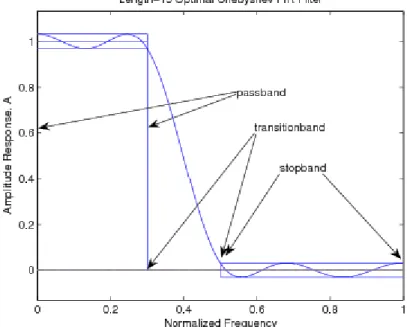
In signal analysis it is desirable to remove unwanted frequencies and only keep the frequency spectrum of interest, that is, to filter the signal. There are various filters for different purposes. All filters will allow some frequencies to pass, the pass-band, and will suppress some frequencies, the stop-band, with the transition between these two being called transition-band, as seen in figure 2.3. A low-pass (LP) filter will attenuate signals with frequencies higher than the cutoff frequency and the lower frequencies will pass unchanged. The attenuation depends on the order of the filter, thus a high order filter will attenuate the higher frequencies more than a low order filter. Generally the signal is attenuated 20*n dB per decade or 6*n dB per octave, i.e. how steep the slope in the transition-band is, where n is the order of the filter. The high-pass (HP) filter is the opposite of the LP filter, it allows high frequencies to pass and attenuates frequencies lower than the cutoff frequency. Other types of filters are available but not relevant for this work.
Figure 2.3: The different frequency response bands for a low-pass filter. Source: http://cnx.org/content/m16895/latest/figC0.png (last visit 2012-11-20)
2.6 FPGA
A Field-Programmable Gate Array (FPGA) typically contains fixed function logic blocks, consisting of multipliers and embedded block ram, and programmable logic blocks, typically consists of flip-flops and Look-Up-Tables (LUTs), together with a programmable interconnect connecting the logic blocks together. The programmable logic block is the basic unit of the FPGA, also referred to as slice, logic element or logic cell, among others. The FPGA is configured using a hardware description language (HDL). A design tool is used to convert the HDL into a bitstream for downloading to the FPGA.
2.7 SoC
System on Chip (SoC) is an electronic system embedded on a single chip. An SoC usually consists of a combination of microcontroller/microprocessor/DSP, memory block, peripherals, external interfaces, timing sources, analog interfaces and others. An FPGA solution made from several IP cores often with a soft CPU core, that controls the system, is an FPGA based SoC. There are solutions with a hard-wired SoC, which often includes a CPU, combined with an FPGA on a single chip, that are called SoC FPGA.
3
Related Work
Contreras-Medina et al., 2008,[7] used a low-cost FPGA when developing a special purpose vibration analyzer with multiple input channels. It was developed because several applications required simultaneous vibration monitoring of multiple-channels and most of the available equipment were not suited for that. An FPGA was used because of its parallel architecture, reconfigurability and the ability to become an SoC solution.
The solution consists of two parts; an instrumentation system and the FPGA. The instrumentation system consists of a three-axis accelerometer that senses vibration and its output, acceleration in X-, Y- and Z-direction, are passed to a 4-channel 12-bit ADC, although only three channels are used. The instrumentation system then transmits data on 3-channels in parallel to the FPGA. When the data is received three 1024-point FFT computations are done simultaneously, with a total calculation time of 1.33 ms.
A vibration measurement and analysis instrument was developed by da Costa et al., 2010,[8] that implemented the digital signal processing algorithms e.g. FIR filter, FFT etc onto a low-cost FPGA with the use of a MATLAB/Simulink model. The DSP Builder from Altera was used to automatically create HDL from the MATLAB/Simulink model. The system was developed with the purpose to diagnose the condition of an induction motor so that no trained expert would be required for that task.
The system is built up of five functional blocks; Data acquisition and filter, time domain analysis, vibration severity measurement, critical alarms and frequency domain analysis.
The data acquisition and filter block samples one analog input with a sample rate of 25 kHz, then performs linear scaling of the signal and filters it through a digital 6th order low-pass Butterworth filter with a cut-off frequency at 12 kHz. The signal can then be filtered in a high-pass filter by using one of four predetermined configurations, after which the signal is sent to the time domain analysis block and the frequency domain analysis block. In the time domain analysis block, RMS value, peak value, crest factor and kurtosis are calculated. The Vibration severity measurement block uses the overall RMS level to extract the vibration severity specified by ISO standard 10816-1 and has four outputs of machine status: good, satisfactory, unsatisfactory and unacceptable. In the critical alarm block three outputs of alarm status are displayed and show if the peak value, crest factor or kurtosis is larger than specified alarm levels. In the frequency domain analysis block the signal can be filtered again, but this time in a band-pass filter, using one out of four predetermined configurations before theFFT is calculated and displayed.
4
Problem Formulation
A vibration monitor instrument has been developed for the maintenance market to ensure a higher availability for production equipment. The instrument monitors vibrations and analyzes their frequency patterns by applying numerous algorithms. Due to the high production cost and the need for increased performance of the current design, a new version is planned. The aim of this work is to find a method to translate the existing processing system composed of both analog and digital components into a mostly digital system using an FPGA and show the viability of that method. The main goal of the new version is to increase performance and decrease the production cost.
The solution needs only be a proof of concept on an FPGA of one functional vibration input channel. In this work focus should be on the measurement module.
5
Analysis of Problem
The new system has to fulfill the requirements of the existing one and in addition be more responsive and cost less. First the structure of the existing system is given and then some characteristics are presented. The vibration monitor instrument consists of a CPU-module and up to 10 measurement modules.
5.1 Measurement module
5.1.1 Overview
The existing measurement module is made up of two measurement boards, one backplane, one DSP-board and has eight input channels for sensors of vibration or temperature type. The different boards are connected through the backplane. In the system the signal passes through a setup of analog filters, one setup per sensor channel. The signal then passes through an Analog to Digital Converter (ADC) before entering a DSP for FFT and other computations. The result is then sent to the CPU module over EtherCAT for further computation and distribution. Figure 5.1 shows a simplified overview of the system abstracted to one vibration input channel. The separate functional blocks of the system will be explained more thoroughly in the following sections.
Figure 5.1: Abstract overview of the measurement module.
5.1.2 Filter Block
The filter block, in figure 5.2, filters the input signal by removing unwanted frequencies above 12.8 kHz. Before the analog input signal enters the filter block a voltage divider scales the input signal to a suitable level. The analog signal is then divided where one part is mapped to a 1st order HP-filter, to remove the DC part of the signal, and the other to a differential amplifier. The HP-filter outputs a true AC-signal which is again split, with one part being passed to a differential amplifier and the other part to an instrumentation amplifier. The DC-part of the input signal is obtained by differentiating the true AC-signal and the analog input signal, which is used to detect anomalies in the sensor attached to the module. The instrumentation amplifier scales the AC-signal to an appropriate voltage level for the ADC’s input channel. Between the signal leaving the instrumentation amplifier and reaching the ADC it passes through a series of three 2nd order Butterworth LP-filters of Sallen-Key topology making them together act as one 6th order filter. This filter also works as an anti-aliasing filter for the signal.
Figure 5.2: The Filter Block that prepares the input signal for the ADC and separates the DC component from the AC component in the input signal.
5.1.3 ADC Block
The ADC has 8-channels with 16-bit resolution where each channel has a designated sample and hold circuit. In addition each channel contains a 2nd order Butterworth LP-filter with a cut-off frequency at 15 kHz that prevents aliasing since they are sampled at 32 kHz. The ADC block,
shown in figure 5.3, is composed of the ADC and two analog switches. In the figure below it is shown how the ADC block is connected to the input of the system. Four of the ADC channels are connected to the AC-parts of the filter blocks while the other four are either connected to the DC-parts of the filter blocks or temperature-signals. Each temperature signal is filtered with a 2nd order LP Butterworth filter with a cut-off frequency at 30 Hz in order to remove noise from the supply voltage. The choice between the DC-signals and the temperature signals are controlled with the analog switches.
Figure 5.3: Abstract overview of the measurement board and its different blocks, specifically the ADC block. The ADC has eight input channels of which four of them are AC signals and the other are DC or temperature, which are controlled by analog switches.
5.1.4 DSP Block
The DSP block, in figure 5.4, making up the DSP-board, consists of a DSP, EEPROM, SDRAM with input from two measurement boards through the backplane, an inter-board communications board. A measurement board consists of the components shown in figure 5.3 above, with one addition, the Sence1/CS signals. Analysis of the samples from the ADC is performed by the DSP. The analysis at this stage is FFT, peak-to-peak and root mean square etc. The FFT calculation is done on a sample window of 1 second, thus a transform size of 32 768 samples. For the existing system the calculations have taken a couple of seconds.
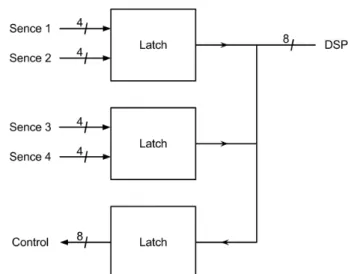
The Sence/CS is a bus that is switched to be either input, sense signals (Sence), or output, control signals (CS). The Sence signals are I/O configurations which are configured with jumpers. The control signals consists of chip-select signals and a control signal for the DC/Temp switch. Four additional signals are taken as input by the DSP, two RPM signals and two steering signals, used for calculations. Results from computations done by the DSP are transmitted through EtherCAT.
Figure 5.4: Shows the I/O connections of the DSP.
5.1.5 I/O configuration and control (IOCC) block
Routing of the I/O configuration signals to the DSP and control signals from the DSP is done over a switched bus system controlled by latches. This allows the DSP to receive input or transmit output depending on the state of the latches, controlled by the DSP. One IOCC block is present in each measurement board. Figure 5.5 below shows how the routing is done on an abstract level where signals are grouped into buses. The I/O configuration signals are labeled Sence and the control- and chip select signals are labeled Control.
Figure 5.5: The latches controls whether the Sence signals to the DSP or if the control signals from the DSP will pass on the bus.
5.1.6 EtherCAT block
EtherCAT is a high performance Ethernet based bus-system and is in this system used to send data between the measurement module and CPU-module. The EtherCAT component used in the measurement module is ET1200 Slave controller.
5.2 System requirements (Measurement module)
An overview of the system requirements are listed, in table 1, for ease of access.
Table 1: The system requirements.
Functional Block Requirement
Filter
Cut-off frequency 12.8 kHz ADC for vibration measurement
Sampling frequency Resolution Simultaneous inputs 32 kHz 16-bit 8 channels ADC for DC measurement
Sampling frequency Resolution
> 1 Hz 12-bit ADC for temperature measurement
Sampling frequency Resolution 10 Hz 12-bit FFT Sample size Transform time 32 768 samples <50 ms
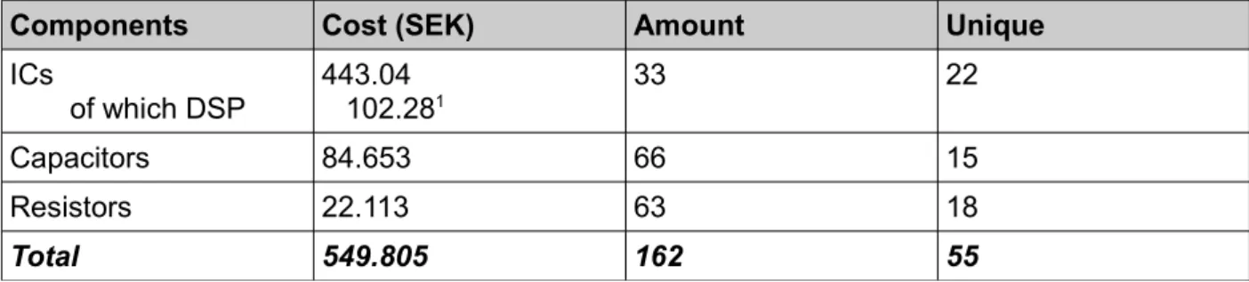
5.3 Component cost (Measurement module)
The measurement module consists of a DSP-board, two Measurement-boards and a Backplane. The amount and cost of components on each board need to be known before changing the system, because the new design decisions depends on it. The cost for the possible new design
need to be compared with the existing design.
The cost and the amount of components for the different boards are summarized in tables 2, 3and 4. Number of unique components are listed since many different types of components will have a negative effect on the price due to mounting costs. For the tables below prices were updated 2012-04-23 unless otherwise specified.
Table 2: Amount and cost for the components on the DSP-board.
Components Cost (SEK) Amount Unique
ICs of which DSP 443.04 102.281 33 22 Capacitors 84.653 66 15 Resistors 22.113 63 18 Total 549.805 162 55 1Price updated 2012-05-25
Table 3: Amount and cost for the components on the Measurement-board
Components Cost (SEK) Amount Unique
ICs of which ADC 912.24 433.4 64 15 Capacitors 24.868 100 13 Resistors 43.524 124 20 Total 980.632 288 48
Table 4: Amount and cost for the components on the Backplane
Components Cost (SEK) Amount Unique
ICs 216.74 17 8
Capacitors 16.846 17 3
Resistors 3.861 11 6
Total 237.447 45 17
The total component cost, for all the boards (DSP-board + 2*Measurement-board + Backplane), is
2748.516 SEK. The total production cost is however unknown for the existing system, but by
reducing the amount of components in the new design, especially unique ones, the production cost will be reduced.
5.4 CPU-module
This module sends requests via EtherCAT to the measurement modules about what to measure e.g. to perform an FFT- or RMS-calculation on the sensory input to measurement module 1. The processed data is then sent from the measurement module to the CPU over EtherCAT. This module forwards the analyzed data to the PC where it is presented in a program called SpectraLive or in a web interface. If the data is viewed in the web interface communication is done over the Ethernet protocol, otherwise RS-232 is utilized.
For some of the more computation-heavy calculations such as envelope and vector calculations the above flow differs in that the actual calculation is performed by the CPU-module itself. In “turbo mode” the FFT calculation will be done in the CPU-module instead of the DSP which reduces the transformation time to 50 ms.
6
Method
There are many existing project methodologies available, with their pros and cons, but the most obvious distinction between them are agile and non-agile methods (waterfall). Since the burden of documentation and the rigid work flow enforced by the waterfall methods could slow down progress, the chosen methodology for this project was according to agile models, with meetings more in the form of discussions during the day. However, to not get lost in the freedom given by the agile method the waterfall model served as an underlying structure of the big picture, giving information of what needed to be done, although the order of the tasks were not strictly followed. The method allowed work to progress on many tasks simultaneously and also jump back and forth between task.
The work consisted of these main parts:
• Study circuit diagrams of the existing system and identify their functional blocks. • Search for replacements to the identified blocks
• Design of the new system
• Find the best suited FPGA/SoC FPGA • Implementation and testing
• Write the report
During the study and system analysis the method of choice has been the break-down approach to identify groups of components making up functional blocks of which some can be exchanged for either digital solutions or altered in other ways to achieve the goals of this work. Each and every block performs some important function within the system.
Possible replacements for identified blocks or groups of blocks of components must maintain the same functionality as the originals, but preferably at a lower cost. A digital replacement could be a component written in HDL or an IP Core implemented on an FPGA but even physical components are possible although a secondary option. Analog replacements are only of interest when they can replace a larger set of components for a smaller set or when the same functionality can be obtained at a lower cost. Due to the above reasons most replacements will be aimed at becoming components in the FPGA.
New system designs must maintain the functionality of the existing system as a whole; meaning the system is treated like a black box, where for a given input the output must be consistent with the existing system. The internal design of the system can be varied.
Searching for the best suited FPGA or SoC FPGA requires estimations of how much resources the components in the design will demand, which is obtained through reading datasheets and by implementing test versions of components. Comparing prices between vendors are also necessary.
Designs found suitable for the system will be in part implemented on an FPGA in order to achieve a proof of concept. Testing has been done on every individual component in the system before they were integrated into the final system. This ensures that the parts of the system are correct in the case of the tested scenarios which increases the possibility that they function correctly after integration into the system.
Documentation of important information and writing on the report has been done continuously during the projects lifetime.
7
Research
Potential replacements for the functional blocks identified during the “Analysis of problem” were researched as a foundation for the design phase. The replacements researched are presented in this section. Each of the replacements has been evaluated in terms of performance, resource usage and cost where possible. Although different implementation options were researched, FPGA based implementations were focused upon, but also the possibility of DSP implementations were considered.
7.1 Filter
Research has been done to better understand analog filters and to see if any analog replacements exists within the performance and cost frames. Digital filters such as FIR and IIR have been researched to obtain knowledge of existing solutions and an understanding of the workings of and how to implement these.
7.2 ADC
Possible replacement alternatives to the ADC in the existing system has to support the desired sampling frequency, resolution and have enough input channels. Research after alternatives have focused on physical hardware components, but also covered the possibility of having ADC IP-cores on an FPGA.
7.3 DSP
Possible options to the current DSP have been researched with focus on other DSP ICs, ARM SoC or having functionality of the DSP done as IP-components on an FPGA. The functionality looked into in more detail has been FFT. In the search for suitable ARM SoCs there are a few requirements that has to be satisfied: enough RAM memory to store data sampled at 32 768 Hz for 1 second, enough on-chip ADCs, sufficient number of I/O pins and low cost.
7.3.1 FFT
The theory of FFT has been studied in an attempt to understand how the transform is calculated and to determine if an implementation from scratch is a viable option. The research also included implementations of FFT on FPGAs as IP Cores.
7.4 EtherCAT
An EtherCAT-controller IP core has been searched for in order to determine the possibility of replacing the current external component with an FPGA implementation.
7.5 FPGA / Soc FPGA
The use of an FPGA or SoC FPGA in order to replace the functionality of physical components, both analog and digital, is a requirement for this project. Due to this a study of available and planned FPGAs and SoC FPGAs have been conducted in order to evaluate possible candidates for this work. Important aspects to evaluate are the amount of resources, such as I/O pins, programmable logic blocks etc., and the cost.
8
Research Results
The results from the research are presented in this section. Research and development of designs were worked on concurrently; a workflow supported by the agile project methodology. There are parts of the research that could not be done until a certain level of knowledge had been achieved. Knowing the number of required input channels are needed to select e.g. certain ADC ICs or FPGA-based ADC implementations.
8.1 Analog Filters
Analog filters come in several types where the first distinction is the division in passive versus active filters. All filters are categorized according to how steep their transition-band is, which is referred to as the order of the filter. The simplest 1st order passive filters are made from any combination of a resistor (R), a capacitor (C) or an inductor (L). Filters can be type categorized as low-pass, high-pass, band-pass or band-stop.
Active filters can be made of any RLC combination together with an active component such as an amplifier. In the existing system the analog filters are active filters, where the LP-filters are 2nd order of Sallen-Key topology and the HP-filter is a 1st order active filter. Analog LP- and HP-filters can be combined in series of the same type, to form higher order filters, or together to form band-pass or band-stop filters. These analog filters give continuous time-domain filtering of signals which is of great value in signal analysis.
8.2 Digital Filters
Digital filters have many advantages over analog filters such as the ability to be reconfigured during runtime and to be of higher order, which allows for a steeper transition between the passband and stopband frequency (roll-off). No external components are required for a digital filter. The properties of a digital filter are determined by values stored in the digital system and will therefore stay unchanged over time, as compared to analog filters were the resistor, inductor and capacitor values can change.[9]
The characteristics of a filter is the filter’s response given an impulse as input. In digital electronics this is valuable since a sampled input signal can be seen as a sequence of consecutive impulses. The output of a filter may be calculated by convolving (briefly described in the FIR description) the input signal with the filter’s impulse response. The response may be of finite length or very long (infinite), which connects to the terminology used for digital filters, Finite Impulse Response (FIR) filter and Infinite Impulse Response (IIR). IIR filters are derived from analog filters and do not give a linear phase response and can also be unstable due to the feedback-loop. FIR on the other hand gives a linear phase but do not originate from analog filters [9]. For digital solutions IIR-filters can be harder to implement [10].
Due to the non-linear phase of the IIR filter they are not of interest for this work since analysis of the phase is part of the system. Therefore only the FIR filter has been studied further; a short description of IIR can be found in Appendix A.
8.2.1 FIR description
A FIR filter [6, 9] is built up of multiply-accumulate (MAC) units and delay elements. The input sample data is multiplied with a coefficient and added together with delayed input samples multiplied by other coefficients. The multipliers that taps the signal from the delay line are called taps. The length of the delay line, number of delay units, determines the order of the filter. A delay line of length N yields an Nth order filter and N+1 taps. Figure 8.1 shows an example of a FIR filter structure where x is input, Z-1 is a delay unit, f is a coefficient and y is the totaled output.
Figure 8.1: Structure of a FIR filter. It consists of delay and MAC units.
The output of a FIR filter is calculated with equation 2 where f are the coefficients, x is the input samples and Lis the number of filter coefficients.
y [n] = x [n ]∗ f [n ] =
∑
k=0 L−1f [n]∗x [n−k ]
n=0,1 , ...
(2)The output y, in equation 2, is said to be obtained by convolving the two functions x and f. Convolving is the act of doing a convolution which is calculating the area overlap in time between two functions.
Coefficients can be calculated using the filter functions in MATLAB or GNU Octave.
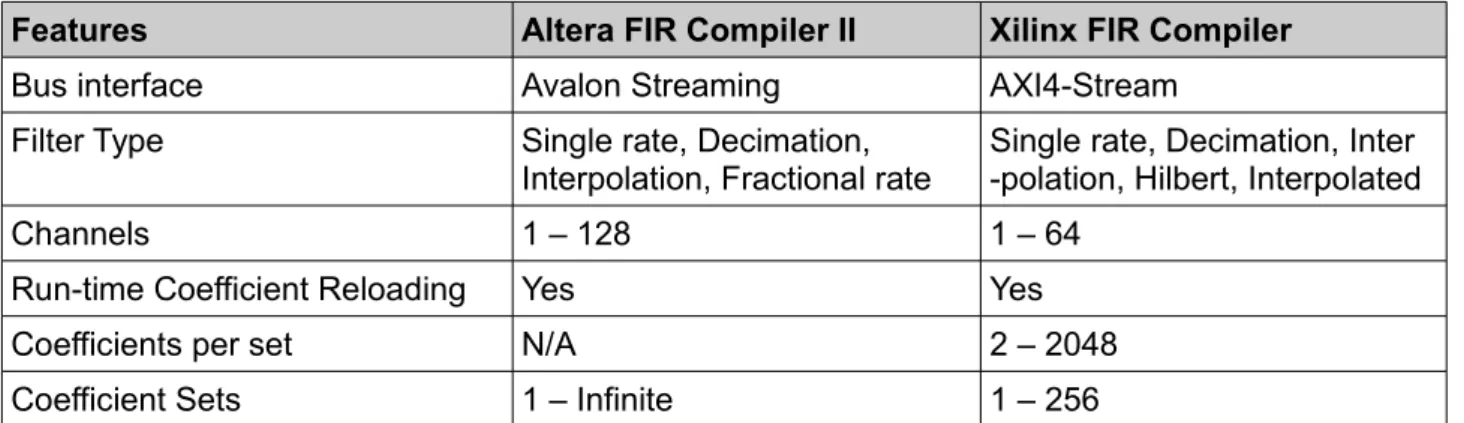
8.2.2 FIR Compilers
Xilinx provides a LogiCORE IP FIR Compiler core for generating FIR filters. A full production license is included with Xilinx ISE Design Suite software tools at no additional charge. The Xilinx ISE Design Suite: System Edition cost 5 195 USD for one year.
Altera also provides a tool for generating FIR filters, the FIR Compiler II MegaCore Function. The full production license is included in an active Quartus II Subscription Edition software which cost 3 995 USD for one year.
The FIR IP cores provided by Xilinx and Altera are optimized for their own FPGA devices. They also provide graphical user interfaces to simplify creation and configuration of the filter’s parameters. Table 5 shows the features of the two different FIR IP cores.
Table 5: Features of Altera’s FIR Compiler II and Xilinx’s FIR Compiler.
Features Altera FIR Compiler II Xilinx FIR Compiler
Bus interface Avalon Streaming AXI4-Stream Filter Type Single rate, Decimation,
Interpolation, Fractional rate
Single rate, Decimation, Inter -polation, Hilbert, Interpolated
Channels 1 – 128 1 – 64
Run-time Coefficient Reloading Yes Yes Coefficients per set N/A 2 – 2048 Coefficient Sets 1 – Infinite 1 – 256
Resource estimations for Altera FIR Compiler II and Xilinx FIR Compiler filter cores are presented in tables 6 and 7. The estimations have been acquired in each design tool by synthesizing the cores. The configuration of the filters are single rate, one channel and 21 coefficients.
Table 6: Resource estimations for Xilinx FIR Compiler on Zynq-7020. Logic Used Flip-flops 152 LUTs 128 BRAM 0 DSP slices 1
Table 7: Resource estimations for Altera FIR Compiler II on Cyclone III EP3C55F484C8.
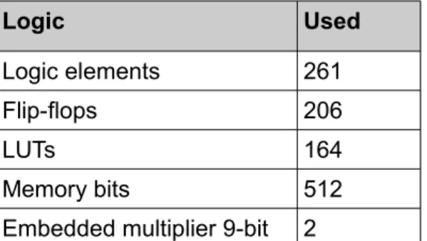
Logic Used
Logic elements 261 Flip-flops 206
LUTs 164
Memory bits 512 Embedded multiplier 9-bit 2
WinFilter is a free software tool used to design digital filters. It can generate C code for both FIR and IIR filters and VHDL code for FIR filters. The VHDL code can be optimized in regards to either size or speed and the software tool will show an estimation of FPGA resource usage. The filters supported are low-pass, high-pass, band-pass or band-stop. The filter models to choose from are Butterworth, Chebyshev, Bessel, Raised Cosine and Rectangular.
8.3 ADCs
8.3.1 Conventional ADC
ADC units were investigated after new designs were made. The new designs call for the use of one 8-channel 16-bit ADC. During the research of ADC ICs two possible alternatives have been found, both from Maxim. Both have 8-channel track and hold (T/H) with a dedicated ADC for each channel followed by 8 registers for holding the conversion values and with parallel output of the result. The ADCs found were the Maxim MAX11046ECB+ and the MAX11049ETN+, shown in table 8.
Table 8: Lists the properties of MAX11046ECB+ and MAX11049ETN+.
MAX 11046 ECB + MAX 11049 ETN +
Resolution 16-bit 16-bit
Input voltage -5V to +5V 0 to +5V
Input bandwidth (MHz) 4 4
Channels 8 8
On-Chip T/H Circuit for Each Channel
Yes Yes
Output interface 16-bit parallel 16-bit parallel Min. Typ. Max. Min. Typ. Max. INL (LSB) > -2 ± 0.4 < +2 -2 ± 0.65 +2 DNL (LSB) > -1 ± 0.4 < +1.2 > -1 ± 0.7 < +1.2 Signal-to-noise ratio (SNR) dB 91 92.3 90.7 92.3
Total Harmonic Distortion (THD)
-105 -98 -108 -98
Throughput rate per channel (ksps)
1 250 1 250
Price1 130.29 SEK2 117.99 SEK2
2 Price for 1000 units as seen in shopping cart
8.3.2 FPGA based ADC
By implementing the ADC on an FPGA some space can be freed up on the circuit board. Research on ADCs implemented on FPGA has been done by several researchers [11, 12, 13]. The common way of implementing ADCs on FPGA is to have an output from the FPGA connected to an RC circuit. The feedback voltage obtained from the RC circuit are then compared with a sampled voltage either using an external analog comparator or a LVDS input buffer on the FPGA. The ADC logic implemented on FPGA differs in all three papers and the solution by Uchagaonkar et. al., 2012, [12] will be described more in detail below.
Figure 8.2 shows the ADC structure which is based on sigma-delta modulation. The components implemented on the FPGA are D Flip Flop, CIC Filter (cascaded integrator-comb), and a Digital Filter. CIC is a special type of FIR filter combined with either an interpolator or decimator; for this design a decimator. The external components used are a comparator, resistor and capacitor. The resistor and capacitor together creates an RC circuit which voltage value is compared to the sampled value using the comparator. If the sampled voltage is larger than the RC voltage the comparator will output value ‘1’, else it will output ‘0’. The flip flop receives the value from the comparator and generates a feedback value to the RC circuit. It also sends the value to the CIC filter. The CIC filter is used for decimation to reduce the sample rate and averages a number of samples. A digital filter is then used to eliminate high frequency noise.
Figure 8.2: An ADC implemented on an FPGA. [12]
Stellamar offers a configurable ADC IP core, Digital ADC, that can be implemented on an FPGA. The only external components needed are resistors and capacitors for a simple reconstruction filter. The architecture of the ADC is shown in figure 8.3 below. A reconstruction filter limits frequencies that can be reconstructed and has a similar task as the anti-aliasing filter; Anti-aliasing filters are used before converting an analog signal into a digital and a reconstruction filter is used to produce a smooth analog signal from a digital one. The Digital ADC supports 10-bits, 12-bits and 14-bits of resolution. For 10-bits of resolution the supported bandwidth is up to 100 kHz, 12-bits supports up to 20 kHz and 14-bits up to 10 kHz. INL and DNL issues are not a problem as this is compensated for with oversampling and removal of unneeded bits. This IP core has a license fee in addition to a royalty for each unit.
Figure 8.3: The architecture of the Digital ADC from Stellamar. Source: http://www.stellamar.com/products.shtml
Xilinx also provides an ADC IP core, bundled with Xilinx EDK, that can be implemented on an FPGA, the XPS Delta-Sigma ADC. This ADC IP core requires a pair of resistors, a capacitor and a comparator as analog external components, as shown in figure 8.4. The supported resolutions are 10-bit and 12-bit. The supported sample rate for 10-bit resolution is up to 4340 Hz and for 12-bit resolution up to 887 Hz. The IP core connects as a 32-bit slave on a PLB v4.6 bus. A full production license is included with Xilinx ISE Design Suite software tools at no additional charge.
Figure 8.4: Xilinx XPS ADC FPGA based design.Source:
http://www.xilinx.com/support/documentation/ip_documentation/xps_deltasigma_adc.pdf
(last visit 2012-11-20)
A Simple Sigma-Delta ADC reference design, shown in figure 8.5, that can be implemented on an FPGA is provided by Lattice Semiconductor. The external components required are resistors and capacitors for a RC circuit. An external analog comparator may be required if the FPGA does not support LVDS input. The ADC supports up to 10-bits of resolution with a bandwidth up to 3.8 kHz.
Figure 8.5: The architecture of Simple Sigma-Delta ADC. Source:
http://www.latticesemi.com/documents/rd1066.pdf (last visit 2012-11-20)
A summary of the different digital ADC IP cores are shown in Table 9.
Table 9: Summary of the digital ADC IP cores.
Provider Resolution Bandwidth FPGA Resource Usage
Stellamar 10-bit 12-bit 14-bit DC – 100 kHz DC – 20 kHz DC – 10 kHz
1195 LUTs, 9 DSP48A1s (Spartan-6 LX75) -Xilinx 10-bit 12-bit DC – 1.7 kHz DC – 346 Hz
111 Slices, 190 LUTs (Spartan-6 LX45) 96 Slices, 204 LUTs (Spartan-6 LX45) Lattice Semiconductor 8-bit 10-bit DC – 3.8 kHz DC – 3.8 kHz 62 LUTs (MachXO2)
8.4 DSP Replacements
Replacements for the DSP found during research will be presented in this section. This comprises details about various ARM SoCs, tables 10 and 11, and the configurability of FFT IP cores from Altera and Xilinx. Note that the replacements only consider the DSP functionality of the existing system, therefore the FIR filter is not included.
8.4.1 ARM SoC
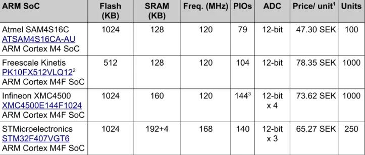
Table 10: ARM SoC units replacing the DSP. One of them does not have a floating point unit, but the other three does; denoted by the ‘F’ in the name of the core, Cortex M4F. All of them have DSP extensions.
ARM SoC Flash
(KB)
SRAM (KB)
Freq. (MHz) PIOs ADC Price/ unit1 Units
Atmel SAM4S16C
ATSAM 4 S 16 CA - AU
ARM Cortex M4 SoC
1024 128 120 79 12-bit 47.30 SEK 100
Freescale Kinetis
PK
10 FX 512 VLQ 12 2 ARM Cortex M4F SoC
512 128 120 104 12-bit 78.35 SEK 1000
Infineon XMC4500
XMC 4500 E 144 F 1024
ARM Cortex M4F SoC
1024 160 120 1443 12-bit x 4
73.62 SEK 1000
STMicroelectronics
STM 32 F 407 VGT 6
ARM Cortex M4F SoC
1024 192+4 168 140 12-bit x 3
65.27 SEK 250
1 Prices updated 2012-11-01
2 One IC in the K10P144M120SF3-family of ICs
Table 11: Available on-chip peripheral control interfaces for the ARM SoC units.
ARM SoC I2C SPI Ethernet UART USB CAN
Atmel SAM4S16C ARM Cortex M4F SoC 2 3 0 2 1 0 Freescale Kinetis2
PK10FX512VLQ12, ARM Cortex M4F SoC
2 3 0 6 0 2
Infineon XMC4500 XMC4500E144F1024 ARM Cortex M4F SoC
61 61 1 61 1 3
STMicroelectronics STM32407407VG ARM Cortex M4F SoC
3 3 1 2 2 2
1 There are six universal serial interface channels usable as UART, double-SPI, quad-SPI, I2C etc. 2 Also has two I2S interfaces
8.4.2 FFT IP
The implementation of the DFT algorithm can be done in a DSP or CPU, but also on an FPGA. During the study of the FFT algorithm different approaches to the computation of the FFT, along with optimizations to speed up the process were found [14, 15, 16]. Implementing the algorithm from scratch turned out to be beyond the scope of this project. Altera and Xilinx both provide core generators for creating FFT IP cores, shown in table 12. These tools allows for customization of the core regarding transform size, data format, precision of the data and architecture etc. Production licenses are included with a license for Xilinx ISE Design Suite software tools and with an active Quartus II Subscription Edition software respectively, at no additional charge.
Table 12: Configuration possibilities for Altera’s FFT and Xilinx’s FFT.
Features Altera FFT Xilinx FFT
Bus interface Avalon Streaming AXI4-Stream Transform size 64 – 65 536 8 – 65 536
Channels 1 1 – 12
Run-time configurable transform length
Yes Yes
Input data width 8 – 32 8 – 34 Output order Natural order, Bit reverse
order
Digit reversed order, Bit reversed order, Natural order Rounding output Truncation, Convergent
rounding 1
Truncation,
Convergent rounding Architectures Streaming, Variable
Streaming, Buffered Burst and Burst
Pipelined Streaming, Radix-4 Burst, Radix-2 Burst and Radix-2 Lite
1 The architecturedetermines which rounding method will be used; Convergent rounding is used for variable streaming and truncation is used otherwise.
Resource estimations for Xilinx FFT IP core are presented in table 13 and for Altera FFT IP core in table 14. The estimations have been acquired in each design tool by synthesizing the cores. The configurations are shown in Appendix A.
Table 13: Resource estimations using Xilinx Fast Fourier Transform core on Zynq-7020 for some of the different architectures with a transform size of 32 768. For more detailed information on the configuration options used see Appendix A.
Architecture Used
Resource Pipelined Streaming Radix-4 Burst Radix-2 Burst Radix-2 Lite
Flip-flops 6722 2756 1379 1101
LUTs 6415 2731 1438 981
BRAM (36 Kb) 38 42 33 36
DSP slices 21 9 3 2
Transform Cycles 98 467 131 239 311 549 557 146
Table 14: Resource estimations using Altera FFT MegaCore function on Cyclone III EP3C55F484C8 for the four different FFT architectures, all with a transform size of 32 768. For more information on the configuration used see Appendix A.
Architecture Used
Resource Streaming Variable Streaming Buffered Burst Burst
Logic elements 7480 14 547 7 492 7 388
Flip-flops 6 427 11 563 6 472 6 367
LUTs 6 074 9 482 5 378 5 351
M9K 541 149 427 200
Memory bits 4 980 992 1 369 372 3 932 416 1 835 264
Embedded multiplier 9-bit 48 104 48 48
Block Throughput Cycles 32 768 32 768 36 864 94 355
8.5 EtherCAT
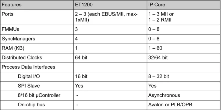
Beckhoff Automation provides an EtherCAT Slave Controller IP core that can replace the existing EtherCAT ET1200 Slave Controller. The EtherCAT IP core is configurable, making it possible to use the same configuration as for the ET1200 or another better suited configuration. Table 15 list the features of ET1200 and the IP Core solution.
Table 15: Characteristics of ET1200 and IP Core EtherCAT controllers.
Features ET1200 IP Core
Ports 2 – 3 (each EBUS/MII, max- 1xMII) 1 – 3 MII or 1 – 2 RMII FMMUs 3 0 – 8 SyncManagers 4 0 – 8 RAM (KB) 1 1 – 60
Distributed Clocks 64 bit 32/64 bit Process Data Interfaces
Digital I/O 16 bit 8 – 32 bit
SPI Slave Yes Yes
8/16 bit µController - Asynchronous On-chip bus - Avalon or PLB/OPB
The EtherCAT IP core is available for both Altera FPGAs and Xilinx FPGAs. Estimated resource usage, in table 16, of the IP core, with the same configuration as for ET1200, on an Altera FPGA and a Xilinx FPGA has been calculated using values given in the EtherCAT IP core Altera Datasheetand EtherCAT IP core Xilinx Datasheet.
Table 16: Estimated resources required of the EtherCAT Slave Controller IP core.
Feature Altera Cyclone III Xilinx Spartan-6
Logic elements M9K Slices BRAM (18 Kb) Flip-flops LUTs
1xMII 900 - 150 - 400 500
3x FMMUs 1950 - 600 - 1200 1350
4x SyncManagers 2200 - 600 - 800 1600
DPRAM (1 KB) 200 1 50 1 0 450
Distributed Clocks (64 bit) 6200 - 1600 - 3600 3900 Digital I/O (32 bit) 250 - 100 - 200 200
SPI 350 - 100 - 250 300
Avalon 200 - - - -
-PLB - - 150 - 400 250
Total: 12250 1 3350 1 6850 8550
There are different licenses for the IP core depending on how and what it should be used for. The price is not available for the EtherCAT IP core and the IP core can only be purchased by members of the EtherCAT Technology Group who have signed an EtherCAT Technology Family License Agreement. For this reason it is assumed that the price for the EtherCAT IP core is the same as for ET1200.
An evaluation license for the IP core, which is full-featured but time-limited, is available for members of the EtherCAT Technology Group.
8.6 Estimation of total FPGA resource usage
This section contains the estimated resource usage of IP cores on Altera and Xilinx FPGAs, shown in table 17.
Table 17: FPGA resource usage for different IP cores. The FFT configurations are found in table 14, under Streaming and Burst architecture and table 13, under Pipelined Streaming and Radix-2 Lite architecture. The estimated total resource usage is the accumulated resource estimation for the IP cores, FIR, FFT, ADC and EtherCAT.
Core Altera Xilinx
FIR 261 LE 206 flip-flops 164 LUTs 512 bits 2 Multipliers (9-bit) 152 flip-flops 128 LUTs 1 DSP slice FFT
min. max. min. max.
7 388 LE 6 367 flip-flops 5 351 LUTs 1 835 264 Memory bits (1792.25 Kb) (200 M9K) 48 Multipliers (9-bit) 7 480 LE, 6 427 flip-flops, 6 074 LUTs, 4 980 992 Memory bits (4864.25 Kb) (551 M9K) 48 Multipliers (9-bit) 1 101 flip-flops 981 LUTs 36 BRAM (1296 Kb) 2 DSP slices 6 722 flip-flops 6 415 LUTs 38 BRAM (1 368 Kb) 21 DSP slices FPGA based ADC N/A 96 Slices 204 LUTs EtherCAT 12 250 LE 12 250 flip-flops 1 12 250 LUTs 1 1 M9K 3 350 slices 6 850 flip-flops 8 550 LUT 1 BRAM(18 Kb size) Total
min. max. min. max.
19 899 LE 18 823 flip-flops 17 765 LUTs 201 M9K (1 809 Kb) 50 Multipliers (9-bit) 19 991 LE 18 883 flip-flops 18488 LUTs 552 M9K (4 968 Kb) 50 Multipliers (9-bit) 8 103 flip-flops 9 863 LUTs 37 BRAM (1 332 Kb) 3 DSP slices 13 724 flip-flops 15 297 LUTs 39 BRAM (1 404 Kb) 22 DSP slices 1An assumption based on the fact that one logic element in Cyclone III consists of one flip-flop and one LUT.
8.7 FPGA/SoC FPGA
FPGA/SoC FPGA devices were researched and some selected based on the estimated resource usage for all the IP cores. The devices found, with enough resources, were Altera Cyclone III, Xilinx Spartan-6and Xilinx Zynq.
8.7.1 Altera Cyclone III
Cyclone III is the third generation in the Altera Cyclone FPGA series and offers high performance at low power and low cost. The Cyclone III consists of up to 120k logic elements, 432 embedded memory blocks at 9 Kb each making it a total of 3 888 Kb, 531 I/O pins and 288 embedded 18-bit x 18-bit multipliers that can be used for an efficient implementation of DSP algorithms. Each logic element contains one flip-flop and one LUT.
8.7.2 Xilinx Spartan-6
Spartan-6 gives a balanced trade-off between high performance and low cost and is widely used in the industry. The FPGA has up to 23 038 slices, where each slice consists of four LUTs and eight flip-flops, 268 block RAMs at 18 Kb each corresponding to 4 824 Kb, 576 I/O pins and 180 DSP slices. A DSP slice is a piece of dedicated hardware consisting of an 18×18 multiplier and a 48-bit accumulator. DSP operations are costly to implement in the logic of the FPGA, which is the reason for dedicated DSP slices.
8.7.3 Xilinx Zynq-7000
The Zynq-7000 is a new SoC FPGA containing a dual core ARM Cortex-A9 including many communication controllers. The ARM cores have 64 KB L1 cache, 512 KB shared L2 cache, a 256 KB scratch memory and can work at 1 GHz. Among the controllers are two Gigabit Ethernet controllers and two USB 2.0 controllers. Within the ARM cores there are the Jazelle engine for Java bytecode, the NEON media-processing engine for advanced DSP calculation, doing up to 16 parallel executions, and a single precision and double precision vector floating point unit. The bus system used both in the ARM system as well on the FPGA is the AMBA AXI-bus. The FPGA is part of Xilinx 7th generation architecture and contains two 12-bit ADCs in hardware with up to 17 differential inputs. It can contain up to 54 650 slices, where each slice consists of four LUTs and eight flip-flops, 2 180 KB block RAM (545 blocks at 36 Kb) and 900 DSP slices. The DSP slices on the Zynq-7000 are made up of one 18×25 two’s complement multiplier and an accumulator 48-bit, both able to operate at up to 741 MHz.
8.7.4 Microsemi SmartFusion
The SmartFusion was suggested as a candidate at the beginning of the project due to its special blend of SoC, FPGA and programmable analog logic. The SoC has at its core an ARM Cortex M3 which does not have any floating point unit nor DSP extensions. The amount of available SRAM is 64 KB, 512 KB flash memory and the SoC ADC units (up to 3 units) have 12-bit resolution. Its maximum working speed is 100 MHz. The most powerful IC has 24 blocks of of 4608 bits RAM totaling 110 592 bits available RAM, 11 520 flip-flops, 128 I/O and 500k system gates on the FPGA part.
8.7.5 Summary
A summary of the different FPGA families mentioned, where the maximum resources available for the shown devices and additional CPU related information in case of a SoC FPGA is presented in tables 8.14 and 8.15.
Table 18: Maximum available resources for two FPGAs and two SoC FPGAs. The numbers are however not always comparable because the resources contained in a slice, logic gate, or system gate are not the same, in fact they can differ between FPGAs from the same vendor.
Name FPGA Type Slices /
logic elements
flip-flops LUTs Block RAM (Kb)
DSP slices / dedicated multipliers
I/O pins
Altera Cyclone III FPGA 120k 120k 120k 3 888 288 531 Xilinx Spartan-6 FPGA 23k1 184k 92k 4 824 180 576 Xilinx Zynq-7000 SoC FPGA 54.6k1 437.2k 218k 19 620 900 362 Microsemi
SmartFusion
SoC FPGA 500k2 11.5k N/A 110 592 N/A 128
1 One slice contains four LUTs and eight flip-flops.
2 This is not equivalent to slices/logic elements; in the datasheet they call it system gates.
Table 19: A summary of the CPU parts of the two SoC FPGAs.
Name CPU RAM Cache CPU freq. (MHz) DSP ext. FPU1 ADC I/O pins
Xilinx Zynq-7000 ARM Cortex-A9 256 KB 2*64 KB L1, 512 KB L2 1000 Yes Yes 2 130 Microsemi SmartFusion ARM Cortex-M3 64 KB N/A 100 No No 3 41
1 FPU = Floating Point Unit
8.7.6 FPGA prices
Prices for some specific units from the FPGA and SoC FPGA families above provided by different vendors, are shown in table 20.
Table 20: Comparison of FPGA and SoC FPGA programmable logic capacity and prices. Prices were updated 2012-11-08.
Name slices/logic elements DSP Slices Block RAM
(Kb)
Price
Altera Cyclone III – EP3C55F484C8N
55 856 156 2 340 $ 141.50 Altera Cyclone III –
EP3C80F484C8N 81 264 244 2 745 $ 223.00 SPARTAN 6 XC6SLX45-3CSG324C 6 822 58 2 088 $ 57.19 SPARTAN 6 XC6SLX75-2CSG484C 11 662 132 3 096 $ 94.56 Zynq7000 XC7Z020CLG400 13 300 220 5 040 $ 1541 SmartFusion A2F500M3G-FGG256 500k (2) N/A 108 $ 47.40
1 The price is only an estimate and the product is still new on the market.
8.7.7 Peripherals
The system used several different means to communicate between components and modules. A comparison of the relevant peripheral controllers available for each unit is shown in table 21.
Table 21: Comparison of device peripheral abilities.
Device Package I2C SPI Ethernet UART USB CAN
Cyclone III EP3C80F484C8N 0 0 0 0 0 0
SPARTAN 6 XC6SLX75-2CSG484C 0 0 0 0 0 0
Zynq7000 XC7Z020CLG400 2 2 21 2 2 2
SmartFusion A2F500M3G-FGG256 2 2 12 2 0 0
1 GigaEther, 10/100/1000 Mb/s controllers 2 10/100 Mb/s controller
9
System designs
The different design variations originates from the same abstract design, figure 9.1 i.e. the vibration signal enters the ADC preparation block and is converted into digital form by the subsequent ADC. Analysis of the signal can then be performed in the FPGA, which is a conceptual design unit representing different FPGA based solutions presented in the designs, Design 1, 2, 3 and 4.
Figure 9.1: Abstract overview of the proposed system in a measurement module.
9.1 ADC Preparation block
Each design proposal uses the same design for the signal preparation block, shown in figure 9.2. The change in the new design from the existing design is that the analog 6th order LP Butterworth filter is exchanged for a digital filter in the FPGA and an analog 2nd order anti-aliasing filter has been inserted.
Figure 9.2: The ADC preparation block filters out the DC component and prepares the input signal for the ADC.
9.2 Temperature block
The temperature signal in the existing system is filtered with a 2nd order LP filter with a cut-off frequency of about 30 Hz that removes 50 Hz supply voltage noise. A simplification of this 2nd order filter to a 1st order filter with a cut-off frequency of 15 Hz is proposed in the new design. This filters out the unwanted supply voltage noise and reduces the amount of unique components within this filter.
9.3 Shift register
Shift registers on an FPGA can replace the latches used to control the Sence and CS data flow if needed. This need is dependent on the I/O resources available on the processing unit. One of the shift registers receives a parallel bit stream of a certain width and outputs it serially, that is a parallel to serial conversion. The other shift register works the other way around, serial to parallel conversion.
9.4 Design 1 (SmartFusion)
In this conceptual design, figure 9.3, the high-order LP-filter and switching of chip-select signals are conceived to be implemented on the FPGA. The ARM would perform less demanding calculations. An external 16-bit ADC is used to digitize the AC signal and two on-board 12-bit ADCs are used to digitize the DC- and temperature signals. Shift registers are implemented in the FPGA together with a FIR filter. The ARM Cortex M3 performs peak-to-peak and RMS calculations and the result is passed on to the EtherCAT controller. Note that the design does not include FFT, hence the task is passed on to the CPU.
Figure 9.3: SmartFusion based design where two 12-bit ADCs are on-chip. Only basic calculations can be performed by this system.
9.5 Design 2 (FPGA+DSP)
This design is based on an FPGA in tandem with a DSP unit where the filtering and possibly demanding calculations like FFT are performed in the FPGA, shown in figure 9.4. Less resource demanding calculations such as peak-to-peak and RMS are done in the DSP. Note that the DSP is only a conceptual unit performing digital signal processing. Neither the DSP nor FPGA contains ADCs, therefore required ADCs are shown as external components. A 16-bit ADC is needed for the vibration signal and a 12-bit ADC is needed for the temperature signal in order to meet the system requirements. For the conversion of the DC signal a 12-bit ADC provides enough resolution. The DSP acts as a master and transmits analyzed data over EtherCAT.
Figure 9.4: DSP and FPGA combined; The DSP does basic computation whereas the FPGA does more advanced computation.
9.6 Design 3 (FPGA)
This design, figure 9.5, based on having as much functionality as possible in an FPGA requires more logic blocks, memory blocks, LUTs etc. Resources has to be shared between a soft IP core DSP and all other components. For this design a 12-bit ADC is intended to be implemented on the FPGA and also an EtherCAT controller, while a 16-bit ADC will still be in use as an external component. The 12-bit ADC converts the DC and temperature signals whereas the 16-bit ADC converts the vibration signal.
Figure 9.5: An all FPGA based design with as much as possible performed by the FPGA.
9.7 Design 4 (Zynq-7000)
The Zynq design requires an external 16-bit ADC due to the resolution requirement for the vibration signal and 12-bit ADCs are used for both the DC- and temperature signals. FFT, FIR, EtherCAT-controller and other digital components could be implemented in the programmable logic. The Dual Core ARM Cortex-A9 controls the measurement module while also performing several computations for signal processing, as shown in figure 9.6.
Figure 9.6: The 16-bit ADC for the AC signal remains external to the Zynq-7000 unit while the unit can take care of the other conversions, system management and all calculations in its programmable logic and ARM Cortex-A9 dual cores.
9.8 CPU-Module
This module has no new designs but a couple of concept ideas. In order to increase computational power the current CPU-card, which is ARM9 based, could be exchanged for an SoC FPGA with dual ARM Cortex-A9 on-board. For this to be viable the SoC FPGA needs to have the same type of communication controllers on-chip that the present card holds. Another way is to exchange the card for an ARM SoC that does what the current ARM9 based card does.
10 Implementation
The hardware and software implementation will be presented in this section. First the development boards and an overview of the design tools used will be presented.
10.1 Development Boards
Two development boards, table 22, were used during the thesis: the Atlys Spartan-6, figure 10.1, and ZedBoard Zynq-7000, figure 10.2.
Table 22: Lists the features of Atlys and Zedboard.
Features Atlys ZedBoard
FPGA/SoC FPGA Spartan-6
XC6SLX45-CSG324-3 Zynq-7000 XC7Z020-CLG484-1 Memory 128 MB DDR2 16 MB Quad-SPI Flash 512 MB DDR3 256 Mb Quad-SPI Flash 4 GB SD card
Display Two HDMI video input ports
Two HDMI output ports
HDMI output VGA output 128×32 OLED display Communication USB-JTAG 10/100/1000 Ethernet USB-UART USB-HID USB-JTAG Programming 10/100/1000 Ethernet USB OTG 2.0 USB-UART
GPIO 8 user LEDs
6 push buttons 8 slide switches
8 user LEDs 7 push buttons 8 slide switches
Figure 10.1: The Atlys development board. Figure 10.2: The ZedBoard development board.
10.2 Design Tools
The design tool used for implementation was Xilinx ISE Design Suite: System Edition, which includes different software tools shown in table 23.