Abstract— This report presents the use of graphene as a diffusion barrier to a eutectic Ga-In-Sn alloy, i.e., galinstan, for electrical contacts in electronics. Galinstan is known to be incompatible with many conventional metals used for electrical contacts. When galinstan is in direct contact with Al thin films, Al is readily dissolved leading to the formation of Al oxides present on the surface of the galinstan droplets. This reaction is monitored ex-situ using several material analysis methods as well as in-situ using a simple circuit to follow the time-dependent resistance variation. In the presence of a multilayer graphene diffusion barrier, the Al-galinstan reaction is effectively prevented for galinstan deposited by means of drop casting. When deposited by spray coating, the high impact momentum of the galinstan droplets causes damage to the multilayer graphene and the Al-galinstan reaction is observed at some defective spots. Nonetheless, the graphene barrier is likely to block the formation of Al oxides at the Al/galinstan interface leading to a stable electrical current in the test circuit.
Index Terms—Contact, diffusion barrier, graphene, galinstan. I. INTRODUCTION
TRETCHABLE electronics is expected to target a broad range of unprecedented applications that cannot be offered by rigid electronic products [1]. The realization of stretchable electronics requires novel materials that can meet demands in mechanical, electrical, and chemical aspects. Galinstan, a benign liquid eutectic alloy that consists of gallium, indium, and tin, has been considered a new class of liquid metal to replace the toxic mercury [2]. Being a stable liquid in the temperature range from -19 to 1300 oC and with a high conductivity of 3.5×10⁶ S/m at 20 oC, galinstan is indeed a promising stretchable conductor [3]. Metallization on silicone rubber using galinstan for stretchable electronics has been demonstrated [4]. However, galinstan can be problematic when it is brought to contact with many conventional metals [2,3,5]. For instance galinstan readily attacks Al, Ni, and Pt at This work was partially supported by a generous donation of Knut & Alice Wallenberg Foundation through the project “Swedish Graphene Initiative” and by Swedish Strategic Research Foundation (SSF) through the project “Scalable Nanomaterials and Solution Processable TEGs.”
P. Ahlberg, S. H. Jeong, S.-L. Zhang and Z.-B Zhang are with the Division of Solid State Electronics, Department of Engineering Sciences, Uppsala University, Uppsala, 75237, Sweden (e-mail: zhibin.zhang@ angstrom.uu.se). S. H. Jeong, M. Jiao, Z. Wu are with the Division of Microsystem Technology Department of Engineering Sciences, Uppsala University, Uppsala, 75237, Sweden.
U. Jansson is with the division of Inorganic Chemistry, the Department of Chemistry, Uppsala University, Uppsala, 75237, Sweden.
room temperature (RT) [3]. Even Au can be attacked by galinstan although at a much slower pace than those other metals. Graphene, a hexagonal monolayer consisting of sp2 hybridized carbon atoms, is considered another type of material for stretchable electronics due to its exceptional mechanical, chemical, electrical, and electronic transport properties [6]-[9]. It is extremely flexible, elastic, and optically transparent. It has been found that graphene is impermeable to molecules and atoms which can be used to prevent oxidation and corrosion of a material [10]. It has, as a result, attracted intensive attention for future electronic products.
Therefore, it is straightforward to conceive a combination of galinstan and graphene for reliable contacts and interconnects in device fabrication and electronic assembly. One application is to provide a heterojunction solution connecting electronic components and galinstan wiring with graphene as a protection layer. For this purpose, graphene should be chemically inert and physically impermeable to galinstan. Since galinstan is aggressive to many materials, it remains to be confirmed if graphene can survive a direct contact with galinstan. In this work, we will show that graphene exhibits a high degree of chemical inertness to galinstan. We will further demonstrate that graphene can be used as a diffusion barrier to effectively protect metals from the attack of galinstan. Since Al is attacked readily once being brought contact with galinstan, it is used as an indicator to assess graphene as diffusion barrier in this work.
II. EXPERIMENTAL
The graphene films were produced by means of low pressure chemical vapor deposition at 1000 °C. Copper foils from Alfa Aesar were used as the catalytic substrate for graphene synthesis. When placed in the furnace, the Cu foil was annealed at 1000 °C for 30 minutes in Ar/H2 atmosphere
in order to reduce surface oxides and contaminants on the Cu surface. Subsequently, methane (CH4) at 1 vol.%
concentration in H2 was introduced to the reaction chamber for
graphene growth. The growth time was 1.5 hour. When the growth cycle was completed, the H2 and CH4 gases were
turned off and the furnace was naturally cooled down to RT. By adopting the commonly used method in the literature [11], the grown graphene was transferred from the Cu foil to other surfaces. Briefly, a layer of Poly(methyl methacrylate)
Graphene as a Diffusion Barrier in
Galinstan-Solid Metal Contacts
Patrik Ahlberg, Seung Hee Jeong, Mingzhi Jiao, Zhigang Wu, Ulf Jansson, Shi-Li Zhang, and Zhi-Bin
Zhang
(PMMA) was spun onto the graphene/Cu as a supportive layer. The Cu foil was subsequently etched off using FeCl3.
After transfer onto a desired surface, the PMMA was then removed from the graphene by repeated acetone wash with stirring at RT. Aluminum films were deposited onto glass substrates by means of electron-beam evaporation or sputtering. Galinstan purchased from Geratherm Medical AG was deposited in air by means of drop casting using a syringe or spray coating using an airbrush. The latter was used to fabricate patterned galinstan, a fine line using a stencil mask in this work. Materials analysis was performed using Raman spectroscopy, scanning electron microscopy (SEM), and electron dispersive spectroscopy (EDS). Electrical measurement was conducted in real-time using an Agilent 34401A multimeter in pulsed voltage mode and the data started to be recorded before and right after galinstan deposition on the Al films. All experiments were performed under ambient condition, unless stated otherwise.
III. RESULTS AND DISCUSSION
When a graphene thin film is transferred onto a piece of Si capped with a thermally grown SiO2 with a thickness of 300
nm, it becomes visible to the naked eye due to interference [12]. Under optical microscope, it is found that the graphene film consists of polycrystalline flakes of 10 µm in size on average. Measured at different spots by means of Raman spectroscopy, the grown graphene thin film is characterized by a much stronger 2D band than the G band and the Lorentzian shape of the 2D peak (bottom curve in Fig. 1). This indicates that single layer graphene (SLG) dominates the film. In addition, the D band originating from graphene defects is very weak confirming that our SLG films grown on Cu are of high quality. When one SLG is placed on an Al surface, the Raman signals have a much lower intensity than that of one SLG on SiO2. The intensity of the Raman signals from the graphene
increase rapidly with increasing the stacking number of SLG. Surprisingly, the ratio of the 2D to the G peak is larger than unity for a stack of multilayer SLG on Al. In Fig. 1, the Raman band of a stack of 3 SLGs on Al is given as an example. In contrast, the 2D/G ratio for a 3-SLG layer stack on SiO2 is less than unity [13]. The difference in 2D/G ratio
for a stack of multilayer SLG on Al and SiO2 is mostly likely
originated from the interaction of graphene with substrates. In order to assess the chemical inertness of graphene to galinstan, a drop of galinstan was cast onto a 3-SLG layer stack on Al and kept still for 7 months. After carefully removing as much galinstan as possible from the graphene surface without damaging the graphene, the Raman bands in Fig. 1 for the 3-SLG interlayer stack that had been underneath galinstan for months (top curve in Fig. 1) essentially exhibit the same features as those of the 3-SLG layer stack without being in contact with galinstan (middle curve in Fig. 1). This comparison shows that graphene indeed is chemical inert to galinstan at room temperature.
The inertness and robustness of graphene in contact with galinstan and the effect of graphene as a diffusion barrier can
be readily assessed by optical microscopy by gently drop-casting galinstan on top of an Al thin film with and without a graphene interlayer (1-layer SLG). Without graphene, a dark stripe-like layer is observed on the otherwise silvery galinstan surface, cf. Fig. 2(a). A dark ring around the edge of the galinstan droplet is visible from the rear side of the sample, see inset in Fig. 2(a). When one SLG is used as the interlayer between galinstan and Al, attack of the Al film by galinstan persists. This is most probably due to leak of galinstan through cracks in the SLG introduced during the transfer process as well as extensive defects present at the grain boundaries of the polycrystalline graphene flakes. When a stack of several SLGs are used, the defective spots in one SLG are most likely covered by the more perfect regions of the SLG overlay, thus blocking the pathway for galinstan to reach Al. This effect is clearly confirmed as shown in Fig. 2(b) where a stack of 3 SLGs as the interlayer is used; the uniform and silvery color of galinstan remains unchanged over 7 months at RT. The color also remained unaltered when the substrate temperature was increased to 150 oC. Since our experiment was conducted under ambient conditions, it is expected that native Ga oxide and Al oxide could instantly form on the surface of the galinstan drop and that of Al thin film, respectively. As shown in Fig. 2(a), the presence of the native Ga oxide and Al oxide at the interface between galinstan and Al does not seem to prevent the Al film from being readily attacked by galinstan. It is unlikely that the native Ga oxide forms a rigid and continuous layer and that the Al native oxide builds a homogeneous layer without pinholes. Hence, the presence of such native oxides is unable to block the diffusion of galinstan towards the underlying Al film and may only contribute with trivial effects on the contact systems investigated in the present work.
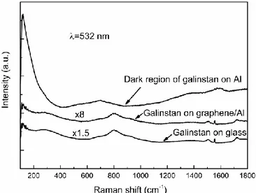
Apart from the optical inspections, the reaction of Al with galinstan can be well characterized using Raman spectroscopy. As shown in Fig. 3, the Raman spectrum from the galinstan drop on Al in the presence of the 3-SLG interlayer stack exhibits essentially the same features as those of a galinstan drop on glass. A broad peak in the low frequency range is observed and can be assigned to the so-called Boson peak [14]. The Boson peak, which reflects the structural features of local or medium-range order, has been observed in liquids [15] and glassy solids [16]. In comparison, the Raman spectrum from the dark region of the galinstan drop on Al, cf. Fig. 2(a), exhibits rather different features with a much stronger low frequency band. The EDS results show that the dark region predominantly contains Al and O. As shown in Fig. 4, the distributions of Al, O and Ga coincide well with each other. In those regions where Al and O are strong in intensity, Ga is barely observable. It is consistent with the previous report, but with other characterization means such as x-ray diffraction [17], in that when Al is brought to contact with galinstan, Al dissolves and reacts with gallium oxide on the surface of the drop and the H2O in air forming
different types of Al oxides, i.e., Al(OH)3, AlO(OH), and
Al2O3, on the galinstan surface.
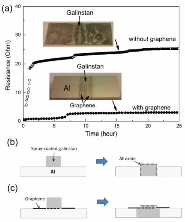
occurs instantaneously leading to the formation of native oxide on the galinstansurface. The oxide “skin” affects dramatically the rheological property of the galinstan drop and results in large contact angles (Fig. 2), which is independent of the wettability of the surface [3]. This makes the formation of a patterned galinstan conductor difficult using the drop-casting method. A well-defined galinstan pattern can, however, be achieved by spray coating using an airbrush. As shown in Fig. 5(a), a fine galinstan line is created on a 400-nm thick Al using this method with polymer stencil masks. Without graphene, the underlying Al is readily attacked by galinstan immediately after the spray coating. In the presence of a 3- or 4-SLG interlayer stack, it is found that the reaction between galinstan and Al still occurs but proceeds much slower. When observed from the rear side of the sample, some reaction spots along the galinstan line start to appear in about 30 minutes after galinstan deposition (Fig. 5(b)) and gradually evolve into a stripe in about 2 hours (Fig. 5(c)). During spraying, numerous tiny galinstan droplets were jetted off the nozzle of the sprayer. The tiny galinstan droplets of high momentum arriving at the graphene surface are likely to impact the weak spots and generate pathways in the galinstan to reach the underlying Al.
In order to electrically assess the effects of graphene as a diffusion barrier, the two-terminal resistor structure shown in Fig. 5(a) was used to monitor, in real time, the resistance variation. Without graphene, a dramatic increase in resistance is observed after the spray-coating of galinstan (open circles in Fig. 6(a)). Prolonging the time ultimately leads to an insulating state with the resistance out of the range of the multimeter, i.e., over 108 ohm. The whole surface of the 400-nm thick Al becomes dark (top inset of Fig. 6(a)) mainly comprising Al oxides according to EDS analysis. The above observations constitute the common features in the evolution of electrical resistance in galinstan/Al without a graphene interlayer. The specific change of electrical resistance over time can vary from sample to sample most likely due to the presence of uncontrollable native Ga oxides on the surface of galinstan as well as uncontrollable amounts of galinstan deposited on Al. Upon galinstan deposition, the underlying Al film is quickly dissolved in galinstan. The associated initial resistance increase is a consequence of Al being replaced by the less conductive galinstan. The dissolved Al diffuses to the galinstan surface and becomes oxidized by gallium oxide and ambient H2O, as confirmed in Fig. 2(a) and Fig. 4. Apparently,
the dissociation of Al by galinstan necessarily proceeds in series with the formation of Al-oxide on the galinstan surface. The insulating Al-oxide layer could extend between the Al leads and the galinstan droplet in-between as illustrated in Fig. 6(b), which is evidenced by the blackish ring along the edge of the galinstan droplet in Fig. 2(b). Although the Al-oxide layer is discontinuous and loose, the current from the left Al lead to galinstan in the middle and then to the right Al lead is expected to quickly decrease. This explains the sharp increase in the two-terminal resistance. The Al thin film on the glass continuously turns into Al oxide under the attack by the deposited galinstan during the electrical measurement and the
entire Al thin film turns to Al oxides in around 3 months after the electrical measurement as shown in the top inset of Fig. 6(a).
When a 4-SLG interlay stack is present on the Al surface, it is observed in Fig. 6 (a) that the two-terminal resistance (solid dots) stays unchanged for around 1.5 hours after galinstan is deposited. Subsequently, a rapid increase in resistance by around 8 times is observed. After this rapid increase, the resistance stays unaltered at 3.0 ohm for an extended period of time. The resistance only increases to 3.5 ohm after more than 3 months. As shown in the bottom inset of Fig. 5, the Al out of the galinstan strip remains unaltered in color. These results clearly show that the graphene diffusion barrier stabilizes the electrical performance of the system under investigation although it does not fully block the galinstan-Al interaction as seen in Fig. 5. Since graphene is highly conductive with a sheet resistance 400 ohm per square for our graphene thin films, the presence of graphene can partly shunt the electrical current. When galinstan is deposited via spray coating, the exposed graphene is partially damaged as described earlier. Assuming that the Al under the partially-damaged graphene is attacked by galinstan and is subsequently oxidized, the electrical current would flow only via the graphene. For an undamaged 1-SLG and 4-SLG of 11 m size, the resistance is 400 and 100 ohm, respectively. In contrast, the resistance for a 400 nm thick Al of the same size is only 0.075 ohm. Therefore, the total electrical resistance can be increased by a factor of 1000 if the Al under the graphene is oxidized. It is thus plausible to suggest that the 4-SLG interlayer stack mechanically blocks the intrusion of the formed Al-oxide into the interface between galinstan and Al as well as the supply of water molecules around the edge of the galinstan for oxidation of Al as illustrated in Fig. 6(c). Hence, the electrical continuity between the two terminals is largely not affected.
IV. CONCLUSION
In summary, we have found that graphene can be an effective diffusion barrier to galinstan that is attractive as a liquid electrical contact for a variety of electronic applications. When galinstan is deposited on Al, the galinstan-Al interaction leads to the formation of Al oxides on the galinstan surface. Graphene is shown to be inert to galinstan that is gently deposited by drop-casting. The graphene also acts as an effective diffusion barrier for preventing the Al from being attacked by galinstan. When galinstan is deposited by spray coating, the high impact momentum associated with the galinstan droplets causes damage to a graphene and the Al-galinstan reaction can be observed at defective spots. Nonetheless, the graphene barrier is likely to block the formation of Al oxides at the Al/galinstan interface leading to a stable electrical current in the test circuit. These findings show a promising application of the combination of galinstan and graphene in electronic assembly. In addition, it also indicates that the combination of galinstan and graphene can be used as reliable contact and interconnect in stretchable electronics. It is therefore important to assess and investigate the barrier effect of graphene to galintan under repeated stress. ACKNOWLEDGMENT
The authors are grateful to Professor Klas Hjort for initiating this work and fruitful discussions, to Dr. Tomas Edvinsson for assisting in Raman analysis, and to Professor Huiming Cheng, Professor Wencai Ren, and Mr. Teng Ma at the Institute of Metal Research, Chinese Academy of Sciences, for sharing knowledge in graphene growth and transfer.
REFERENCES
[1] S. P. Lacour, “Stretchable thin-film electronics” in Stretchable
electronics”, T. Someya, Ed., Germany: Wiley-VCH, 2012, pp. 81-106.
[2] N.B. Morley, J. Burris, L.C. Cadwallader and M.D. Nornberg, “GaInSn usage in the research laboratory,” Rev. of Sci. Instr., Vol. 79, pp.056107, May. 2008.
[3] P. Sen, C.-J. Kim, "Microscale Liquid-Metal Switches—A Review," IEEE Trans. on Industrial Electronics, vol. 56, no. 4, pp. 1314-1330, April 2009.
[4] S. Chen and Z.G. Wu, “Microfluidic stretchable RF electronics,”Lab
Chip, vol. 10, pp. 3227-3234, Aug. 2010
[5] S. H. Mannan and M. P. Clode, “Materials and processes for implementing high-temperature liquid interconnects,” IEEE Trans. Ind. Electron., vol. 27, pp. 508-514, Aug. 2004.
[6] M. Allen, V. Tung, and R. Kaner, “Honeycomb Carbon: A Review of Graphene,” Chem Rev., vol. 110, pp. 132-145, Jul. 2009.
[7] Y. Zhu , S. Murali, W. Cai , X. Li , J. W. Suk , J. R. Potts, and R.S. Ruoff, “Graphene and Graphene Oxide: Synthesis, Properties, and Applications,” Adv Mater., Vol. 22, pp. 3906-3924, Sep. 2010. [8] S. Sarma, S. Adam, E. Hwang, and E. Rossi, “Electronic transport in
two-dimensional graphene,” Rev. Mod. Phys., Vol. 83, pp.407-470, May. 2011.
[9] Lee, W. H., Park, J., Sim, S. H., Jo, S. B., Kim, K. S., Hong, B. H. and Cho, K. “Transparent Flexible Organic Transistors Based on Monolayer Graphene Electrodes on Plastic,” Adv. Mater., Vol. 23, pp. 1752-1756, Feb. 2011.
[10] J. Scott Bunch, Scott S. Verbridge, Jonathan S. Alden, Arend M. van der Zande, Jeevak M. Parpia, Harold G. Craighead, and Paul L. McEuen
“Impermeable Atomic Membranes from Graphene Sheets”, Nano Lett., Vol 8, pp. 2458-2462, Jun. 2008.
[11] X. Li, W. Cai, J. An, S. Kim, J. Nah, D. Yang, et al. “Large-Area Synthesis of High-Quality and Uniform Graphene Films on Copper Foils,” Science, vol. 324, pp. 1312-1314, Jun. 2009.
[12] K. S. Novoselov, D. Jiang, F. Schedin, T. J. Booth, V. V. Khotkevich, S. V. Morozov, and A. K. Geim “Two-dimensional atomic crystals” PNAS, vol 102, pp. 10451–10453, July, 2005.
[13] A. Reina, X. Jia, J. Ho, D. Nezich, H. Son, V. Bulovic, M. S. Dresselhaus, and J. Kong, “Large Area, Few-Layer Graphene Films on Arbitrary Substrates by Chemical Vapor Deposition”, Nano Lett. vol. 9, pp. 30, Jan. 2009.
[14] M. Ivanda, I. Hartmann and W. Kiefer, “Boson peak in the Raman spectra of amorphous gallium arsenide: Generalization to amorphous tetrahedral semiconductors,” Phys. Rev. B, vol. 51, pp. 1567-1574, Jan. 1995.
[15] N. J. Tao, G. Li, X. Chen, W. M. Du, and H. Z. Cumminis, “Low-frequency Raman-scattering study of the liquid-glass transition in aqueous lithium chloride solutions,” Phys. Rev. A, vol. 44, pp.6665-6676, Nov. 1991.
[16] W. B.Jackson, S. J. Oh, C. C. Tsai, and J. W. Allen, “Conduction-Band Density of States in Hydrogenated Amorphous Silicon Determined by Inverse Photoemission,” Phys. Rev. Lett., vol. 53, pp. 1481-1484, Oct. 1984.
[17] J. Ziebarth, J. Woodall, R. Kramer and G Choi, “Liquid phase-enabled reaction of Al–Ga and Al–Ga–In–Sn alloys with water,” Int. J.
FIGURE CAPTIONS
Fig. 1. Raman spectra, measured with a 532 nm laser and placed from the bottom, of a layer of single-layer graphene (SLG) thin film transferred from Cu foil onto SiO2 (1 SLG/SiO2), a 1-layer SLG on Al (1 SLG/Al), a 3-layer
SLG stack on Al (3 SLG/Al) and a 3-layer SLG stack on Al with a remaining galinstan atop (Galinstan/3 SLG/Al), respectively. The signal of 1 SLG/Al is magnified by 20 times.
Fig. 2. Top-view photo of a galinstan drop on a 150 nm thick Al on glass (a) and back-view observed from rear side of glass (inset in (a)), and a galinstan drop on a 3-layer SLG stack/Al on glass where the dashed line indicates the graphene area (b).
Fig. 3. Raman spectra obtained from a galinstan droplet that was cast on a glass (bottom), on a 3-layer SLG stack on Al on glass (middle), and on an Al on glass (top), respectively.
Fig. 4. An SEM/EDS image (top) and three EDS maps which show the distribution of Ga (Lα1 in green), O (Kα1 in red) and Al (Kα1 in light blue), respectively, obtained from the surface of a galinstan drop placed on Al.
Fig. 5. Sketch (left) and top-view photo (right) of a testing structure consisting of a fine galinstan line that was deposited by means of spraying onto a Al film on glass (a) and photos taken from the rear side showing the reaction of Al with galinstan in 0.5 hour (b) and 2 hours (c) after galinstan deposition.
Fig. 6. Two-terminal resistance as a function of time for the testing structure shown in Fig. 5 after the spray-coating of a galinstan line without and with a 4-layer SLG stack interlayer. After more than 3 months, the resistance became too high to measure for the sample without graphene protection while it was 3.5 ohm for the sample with the 4-layer SLG stack, (a). A schematic illustration of the galinstan deposited on the Al thin film without graphene interlayer by means of spray coating (left of (b)) and the subsequent dissolution of Al in the galinstan where a discontinuous and loose Al-oxide layer forms on the surface of galinstan as well as at the interface between Al and galinstan represented by the dash line (right of (b)); a schematic illustration of the galinstan deposited on the Al thin film with the interlayer of 4-layer SLG stack represented by a solid back bold line by means of spray coating where the part of graphene under the galinstan is partially damaged which is represented by the dashed bold line (left of (c)) and the subsequent dissolution of Al in the galinstan where no Al-oxide layer forms at the interface between Al and galinstan (right of (c)).
Fig. 1 Fig. 2 Fig. 3 Fig. 4