Electrochemical etching and anodizing as key stages of surface
treatment of aluminium foil for electrolytic capacitor industry
PAPER WITHIN: Product Development and Materials Engineering. AUTHOR: Harish Appusamy Boopathy, Pavan Kumar Bonthala. TUTOR: Caterina Zanella
JÖNKÖPING, August, 2017.
Application of Electro Chemical Impedance Spectroscopy as non-destructive characterization
of etched anode foil with an anodized dielectric oxide layer.
This exam work has been carried out at the School of Engineering in
Jönköping in the subject area of Functional Materials & surfaces. The
work is a part of the two–year university Master of Science program in
Product Development and Material Engineering under the supervision
of Caterina Zanella and Victor Andoralov of KEMET Electronics AB,
Granna. The authors take full responsibility for opinions, conclusions
and findings presented.
Examiner: Ilia Belov
Supervisor: Caterina Zanella, Victor Andoralov
Scope: 30 credits (second cycle)
Abstract
Abstract
The thesis work has been conducted at KEMET AB in collaboration with surface technology lab at JTH with the purpose of characterisation of the etched anodic aluminium foil as basic sample using anodizing and etching process for the surface treatment.
In the initial stage, the sample preparation was done by using the techniques of Anodic etching and anodic forming processes where a repeated trial and error method of sample preparation headed towards making out a suitable sample set for the purpose of characterization. After this step, the set of 2 different industrial samples were introduced and anodic oxide forming process was carried out in different electrolytes.
In the sample preparations, 4 different electrolytes were used 15% wt. Ammonium Adiphate, 1.5% wt. Ammonium Phosphate, 7% wt. Boric acid and 15% Penta Borate at different stages for performing the anodic oxide forming process. Minimum forming voltages of 20V to a maximum of 100V was employed in the sample preparation and to overcome the waiting time in forming the etched samples a higher current of 0.5A was used.
After the samples preparation, Electrochemical Impedance spectroscopy was used as a tool for characterising the various groups of samples and for observing the micro structures of various samples, they were fractured and the observed on the cross section by SEM.
After the analysis of the etched samples was made, an attempt to compare the results of the data of these samples to that of the 2 set of industrial samples was made and found that the resultant data wasn’t stable enough to characterize since huge scattering were occurring and whereby the simulation of the CPE circuit for the chosen circuit in the analysis was not possible.
Under the analysis, a randomly chosen industrial sample was also used and the resultant data was utilised in understanding the response of the system to different electrolytes.
Abstract
Sammanfattning
Avhandlingsarbetet har genomförts på KEMET AB i samarbete med yttekniklaboratoriet vid JTH i syfte att karakterisera den etsade anodiska aluminiumfolien som grundprov med anodisering och etsning för ytbehandling.
I inledningsskedet gjordes provberedningen med användning av teknikerna för anodisk etsning och anodbildande processer där en upprepad provnings- och felmetod för provberedning ledde ut mot att utarbeta en lämplig provuppsättning med avseende på karakterisering. Efter detta steg infördes uppsättningen av 2 olika industriella prover och anodoxidbildande process utfördes i olika elektrolyter.
I provpreparaten användes 4 olika elektrolyter 15 % vikt Ammoniumadiphat, 1,5 vikt% Ammoniumfosfat, 7 vikt% Borsyra och 15 % Penta-borat vid olika steg för utförande av anodoxidbildningsförfarandet. Minimala formningsspänningar på 20V till ett maximum av 100V användes i provframställningen och för att övervinna väntetiden vid bildning av de etsade proven användes en högre ström av 0,5A.
Efter provberedningen användes elektrokemisk impedansspektroskopi som ett verktyg för att karakterisera de olika grupperna av prover och för att observera mikrostrukturerna i olika prover, de bröts och de observerades i tvärsnittet av SEM. Efter att analysen av de etsade proverna gjordes ett försök att jämföra resultaten av data från dessa prover till den för de två uppsättningarna av industriella prover. Det är konstaterat att de resulterande data inte var stabila nog att karakterisera eftersom stor spridning inträffade och varigenom simuleringen av CPE-kretsen för den valda kretsen i analysen inte var möjlig.
Under analysen användes också ett slumpmässigt valt industriellt prov och de resulterande data användes för att förstå systemets respons till olika elektrolyter.
Summary
Keywords
Surface treatment of aluminum foil for electrolytic capacitor Anodic oxide forming process
Electro chemical etching
Electrochemical impedance spectroscopy (EIS) Capacitance measurement
Contents Contents 1.INTRODUCTION………...7 1.1 BACKGROUND ... ....7 1.2 PURPOSE...8 1.3 RESERACHQUESTIONS ... 8 1.4 DELIMITATIONS...8 1.5 OUTLINE ...9 2.THEORETICAL BACKGROUND...10 2.1 CAPACITORS...10 2.2 ALUMINUM CAPACITORS...11
2.3 ELECTRO CHEMICAL ETCHING PROCESS...12
2.4 ANODIC OXIDE FORMING PROCESS...13
2.5 EIS (ELECTRO CHEMICAL IMPEDANCE SPECTROSCOPY)...13
2.6 CPE (CONSTANT PHASE ELEMENT)...17
3.METHOD AND IMPLEMENTATION…...20
3.1 GROUP1- IN HOUSE SAMPLES ... 20
3.1.1 SAMPLE PREPARATION ………..……….………….20
3.1.2 CLEANING PROCEDURE ……….………..………20
3.1.3 ELECTRO CHEMICAL ETCHING PROCESS………..………..…21
3.1.4 PRE-TREATMENT ……….………..…..……21
3.1.5 PREPARATION OF ELECTROLYTE FOR ETCHING PROCESS ………...22
3.1.6 ELECTRO CHEMICAL ETCHING PROCESS ……….…..22
3.1.7 CAPACITANCE MEASUREMENT ……….……….24
3.1.8 ANODIC OXIDE FORMING PROCESS ……….………24
3.1.9 REPETITION OF THE FORMING PROECSS ………..…27
3.1.10 HEAT TREATMENT PROCESS ……….………..….27
Contents
3.1.13 ELECTRO CHEMICAL IMPEDANCE SPECTROSCOPY (EIS)……….……….29
3.1.14 UPDATED PLAN ……….………31
3.2 GROUP 2 - INDUSTRIAL SAMPLES (BOTH ETCHED & FORMED ANODIC INDUSTRIALLY)...32
3.3 GROUP 3 - INDUSTRIAL SAMPLES OF 90 MICRONS THICKNESS...33
3.3.1 SET-1- FORMING IN 7% wt BORIC ACID……… .………33
3.3.2 SET-2- FORMING IN ALL 3 DIFFERENT ELECTROLYTES ………..……….34
3.3.3 SET-3- FORMING IN ONLY BORIC ACID &AMMONIUM PHOSPHATE ………35
4. FINDINGS AND ANALYSIS ... 39
4.1 DIFFERENT SAMPLES FINDINGS AND ANALYSIS AND THEIR MORPHOLGY…….39
4.1.1 GROUP 1- ANALYSIS OF IN HOUSE ETCHED SAMPLES ...39
4.1.2 MORPHOLOGY OF E8 SERIES SAMPLES ...39
4.1.3 ANALYSIS OF E8 SERIES SAMPLES DATA ...40
4.1.4 ANALYSIS OF INHOUSE ETCHED AND FORMED SAMPLES DATA ...43
4.1.5 MORPHOLOGY OF THE IN HOUSE ETCHED AND FORMED SAMPLES...44
4.1.6 ANALYSIS OF EIS DATA OF IN HOUSE ETCHED AND FORMED SAMPLES…….…….48
4.2 GROUP 2 - ANALYSIS OF INDUSTRIAL SAMPLES...50
4.2.1 MORPHOLOGY OF INDUSTRIAL SAMPLE FORMED AT 46V...51
4.2.2 MORPHOLOGY OF INDUSTRIAL SAMPLES FORMED AT 135V...52
4.2.3 MORPHOLOGY OF INDUSTRIAL SAMPLES FORMED AT 375V...53
4.2.4 ANALYSIS OF THE EIS DATA OF INDUSTRIAL SAMPLES ...54
4.3 GROUP 3 - ANALYSIS OF INDUSTRIAL SAMPLES OF 90 MICRONS THICKNESS...57
4.3.1 ANALYSIS OF EIS DATA OF 90 MICRONS THICK FOIL ...57
4.3.2 MORPHOLOGY OF 90 MICRONS THICK FOIL FORMED IN 15%WT AMMONIUM ADIPHATE……….………60
4.3.3 MORPHOLOGY OF 90 MICRONS THICK FOIL FORMED IN 7% WT BORIC ACID...61
4.3.4 MORPHOLOGY OF 90 MICRONS THICK FOIL FORMED IN 1.5%WT AMMONIUM PHOSPHATE...62
Contents
5. DISCUSSIONS AND CONCLUSIONS...65
5.1 DISCUSSION OF METHOD...65 5.2 DISCUSSION OF FINDINGS ... 67 5.3 CONCLUSIONS ... 69 6.REFERENCES...70 7. SEARCH TERMS... 71 8.APPENDICES... 71 9. LIST OF FIGURES....……….………...76 10.LIST OF TABLES…....……….………….………...78
Introduction
1. Introduction 1.1 Background
Aluminium capacitors are also known as the electrolytic capacitors. Basically, used in functioning of most of the electric and electronic equipment which are used in like computers, vehicles, monitors, screens etc., almost any kind of an electronic circuit board would consist of an aluminium capacitor of either bigger or smaller one’s in size. These types of capacitors are polarized (because of their anodization principle) one’s which uses the pure aluminum foils with an oxidized surface acting as an anode. The anodic oxide forming process which has been done on these etched aluminium foils produces an oxide layer on the porous etched surface, which acts as a dielectric. The etched surface is a porous structure of aluminium which is covered with oxide and then the oxide is in contact with a non-solid electrolyte. Oxide surface is not necessary rough.
The porous surface of the oxide layer is covered by a nonsolid electrolyte serving the purpose of the cathode electrode. But later for making the electrical connection, as the non-solid electrolyte cannot be connected to the electric terminals, an aluminum foil is contacted with the non-solid electrolyte for serving the purpose of cathode electrode.
These aluminum capacitors are basically divided into 3 groups based on the type of electrode materials used in them.
Non-solid aluminum capacitor
Solid manganese di oxide aluminum capacitors Solid polymer aluminum electrolytic capacitors
The first type of aluminum capacitors, the non-solid type are the one’s which are widely used because of their high capacitance ranges (0.1 μ to 2.7F) and also because of their higher operating voltage range of 4V to 630V. These types of capacitors are pretty much inexpensive when compared to the other types of capacitors. [1]
The main motive in the manufacturing of a capacitor is achieving a higher capacitance value for any kind of capacitor being manufactured. Capacitance is the ability to store an electrical charge. Basically, the capacitance of a capacitor is mainly based on the etched surface area of it, since the higher surface area gives a higher capacitance, and so if the etching process is carried out in an optimized way, then the capacitance of the capacitors will be having a high capacitance. [2]
Our thesis runs around the concept of finding how efficient was the etching process of the flat aluminum foils used in the laboratory when compared with the industrial samples which were etched industrially and formed industrially too other than the last set of industrial samples chosen. And, to find out how different would be effect of different electrolytes on anodic oxide forming process and their characterization from the EIS and comparison of all the different group of samples.
Introduction
1.2 Purpose
• Find out if EIS can be used as non-destructive characterization technique of the Al electrodes
• Find an effective solution for the final setup to conclude about the capacitance of an electrolytic capacitor.
• Find an effective relation between the forming and etching at different voltages and times respectively influences the capacitance of an Etched Aluminum foil.
1.3
Research questions
1. How does the etching time influence the capacitance values of the in- house etched samples?
2. How effective is the EIS data of the in house etched samples when compared with the Industrial samples?
3. How does the different electrolytes used for forming the industrially etched samples impact on the characterization when the EIS was done in a different electrolyte from the one used for the forming process?
1.4 Delimitations
In our thesis, we considered the etched samples which had the maximum etching time of 100 seconds and the minimum time of 20 seconds, so the data or the characterization of the samples beyond this range weren’t considered.
The process of anodic forming of the oxide dielectric layer for the in house etched samples is considered between the range of 20 to 100V, and for the industrial samples the range of anodic forming process was limited till 375V. So any characterization beyond these ranges weren’t considered in our project.
Also, the properties of the anodic etching and anodic forming process were confined to the electrolytes used in our project, and any usage of the electrolytes other than the ones used in this project weren’t considered to effect or comparison of the results we achieved.
Introduction
1.5 Outline
The work carried out in the thesis which regards the Application of Electrochemical Impedance Spectroscopy as a non-destructive characterization of etched anode foil with an anodically formed dielectric oxide layer. And also to find how the capacitance is influenced by the anodic etching process and, to characterize the various types by using EIS for following a non-destructive analysis of the samples.
In the first stage, it deals with the samples preparation of the in house etched samples which are etched anodically using different etching times to have a good range of samples for different conditions. These samples were anodically formed later using same time for all the samples under the application of different forming voltages. Capacitance measurements were done and the analysis of these samples was made by employing EIS as a non-destructive test. After the analysis of this set of samples a set of industrially etched and formed samples were also analysed and the attempt for comparing the results of both the first and second sets was made during this stage. And also, an extra set of industrial samples regarding which the details were unknown except the fact that the sample is etched industrially was chosen and anodic forming of it in different electrolytes is carried out in the laboratory at different forming voltages and the EIS was performed on them. In this set, for every sample the eis was made in both same electrolyte used as in anodic forming process and also two other different electrolytes.
In the stage of analysis different samples were analysed and their respective capacitance values were derived by using the analysis software, and the plots were made and the comparison of various samples was tried to perform where it proved that the in-house etching is of lower significance when compared with the first set of industrial samples and also that a lot of improvement must be done for the in house etching process to come up with an optimized sample.
Theoretical Background
2. Theoretical background
In this section we are going to briefly see about the technology behind the capacitors and process of etching and forming.
2.1 Capacitors
Capacitors are passive 2 terminal electrical components which can store a certain amount of electrical energy in a defined electric field (in field where electric influence can be felt). The character of a capacitor is called as Capacitance which is measured in Farads. The unit of capacitance is the ratio of electric charge to the potential difference between the 2 electrodes of the capacitors.
Capacitance,
C = Q/V ... (1)
The structure of a capacitor and its construction varies widely in the practical applications. Most of the capacitors contain 2 electric conductors which are separated by a dielectric medium. This dielectric medium could be vacuum, oxide layer, plastic film etc., Capacitors are used as common parts of electrical circuits. Capacitors are mostly used in the electronic circuits to block DC current and to allow AC current. [3] The capacitors based on their usage point are constructed differently and so they will possess a different outer structure. In general, they all have a same kind of internal structure of how different electrodes are separated by a di electric medium between them. The basic structure in detail of a capacitor could be seen in the following picture (see Figure 1). [3]
The basic principle of how a capacitor works is, as they are consisting of 2 metallic plates with a dielectric medium (could be paper, vacuum, or oxide layer etc,) in
Figure 1: A general construction of the capacitors showing the different layers of it, fetched from [3]
Theoretical Background
created where the positive charge is collected on one plate and the negative on the other. [3]
Applications
These are mostly used in many of the present day electric and electronic components. The main point of application of the capacitors is the energy storage. Capacitors are being used in most of the electric and electronic circuits to fulfil as a temporary battery (since the capacitors can store energy even though they are dis connected from the circuit) when the batteries are being changed. Usage of capacitors as an Amplifier is another important point of application. In the audio system, large capacitors store energy for the amplifiers to use on demand. And in the flash lights capacitors are used to withhold the high voltages. [3,4]
2.2 Aluminium capacitors
Aluminum capacitors or electrolytic capacitors are one of the types which is most used in huge number of electronic devices, Power supplies, DC-DC converters, Photo voltaic cells, Wind power plants etc. Special types of these capacitors are used for energy storage purposes to deliver the output in special forms. [4]
The capacitance of a capacitor is achieved by the process of anodic etching done to the aluminium foil present inside it. The dielectric purpose is served by the oxide layer formed on these etched aluminum foil. The main motive of manufacturing a capacitor is to store the maximum amount of energy and to have a higher capacitance. Our project runs around this step of achieving an optimised etching process and for the etching surface which we obtained we carried out the analysis and compared it to the other industrial samples of different types.
Aluminum capacitor consists of a coil impregnated with the liquid electrolyte and sealed in a can. This capacitor is comprised of an anode foil saturated (etched layer impregnated with an electrolyte.) with a liquid electrolyte and a cathode foil. To separate anode and cathode, a paper foil is place in the middle of the 2. The pure aluminum etched foils have trench tunnels surface which are millions in number formed because of the anodic etching process on them. [3, 4, 11] this etching is performed to increase the surface area since the capacity is proportional to the area. Aluminum capacitors are polar capacitors since and they use the liquid electrolyte, which allows for extremely high capacitance when compared to the other types, but with a small leakage current. In the aluminum capacitors, it may appear the capacitance is between the 2 foils (cathode and anode foils) but, actually the capacitance is lying between the anode foil and the electrolyte, among the dielectric layer formed by the aluminium oxide grown anodically (anodic forming process) on the Aluminium foil. The positive plate is an anode foil, di electric is the insulated aluminum oxide layer on it, true negative plate is conductive which is electrolyte and the cathode foil is connected to the electrolyte and acts as connector and electron carrier. Since the oxide layer is present on the anode, it insulated the anode from the electrolyte
Theoretical Background
The construction of aluminum (electrolytic) capacitors delivers a very large capacitance because of the anodic etching process since it increases the surface area by nearly 100 times, and by maintaining a very close distance between the 2 foils. Their capacitance ranges from o.1 μF to 3F and operating between a voltage range of 5v to 700V. The capacitors operating beyond 550V are available commercially. Based on the variety of the capacitors available in the market, they are sold with a specification mainly revealing about the capacitance and also the operating voltages. Aluminum capacitors are polarized, having distinct positive and negative terminals. [5, 11]
This is because only the foil covered by the oxide can sustain the high positive voltage and the oxide is acting indeed as a protection against the otherwise corrosion process. When it comes to the construction of capacitors they mostly have snap in type, miniature or thermal pack construction, and they’re all built in the form of cylinders. After the processes of etching and forming are done on the aluminum foils, the capacitor elements are rolled up into coils. The anode and cathode are separated by separator papers (mostly 1-4 papers are used), these separate the cathode and anode foils to avoid short-circuit of the system and they later act as a reservoir for the electrolyte. And then the entire setup is pushed into a cylindrical structure. Before or after the winding process is done, the aluminum tabs are attached to the anode and cathode by cold welding process so that they later have a setup in them to be attached onto the circuits. Before these aluminum tabs are punched to the foils, but in these days, they are being cold welded since it reduces the chances of short circuit and performs better in case of high ripple current applications. [5]
2.3 Electro chemical etching process
The current aim of this process is to obtain an etched surface on the flat aluminum foil, whereby the surface area of the foils increases by more than 100 times whereby the coils can have very high capacitances.
This is one of the typical processes which are used to produce roughness on the Aluminum foil used in the electrolytic capacitors. The capacitance of the Aluminum foil is directly proportional to the Surface area of it. But the technique of Electro Chemical Etching process is employed to increase the roughness which is increasing the surface area of the aluminum foil.
Based on the parameters being adapted to the Etching process, the etching profile also varies.
Different parameters on which the etching process is dependent on are: 1. Wave form of the current.
2. Composition of the Solution used to perform the etching process. 3. Temperature.
4. Time
Basically, the etching process is performed in the Chloride solution. And after the process of etching for a certain period, the samples are supposed to be washed thoroughly by the distilled water, so as to remove any kind of chloride residual on it.
Theoretical Background
Because, any small residual of chloride can lead to the corrosion process on the etched surface of the specimen which can cause big disturbance in the functioning. After referring to the 2 articles which had the similar kind of usage regarding the Etching process and the further steps taken in their research, we started up by using the concentrations of the electrolytes which was 1MHCl+5M H₂SO₄ for the etching process. [6, 7]
Unfortunately, as the Aluminum foil what we are using is of 50 Microns thickness, the concentration was too high for this and so the samples got burned. So, we tried to reduce the concentration of H₂SO₄ to 2.5M and even then the samples were burning in the electrolyte after 40 seconds. And so, we finally reduced the concentration of H₂SO₄ to 1M and maintained the concentration of HCl at 1M always, and performed the anodic etching process.
2.4 Anodic oxide forming process
There are many ways to perform the anodic forming process by using different kind of electrolytes. Basically, the forming process is done on the anodic foils. The anode foils of the electrolytic capacitors carry the di electric layer that consist of the aluminum oxide formed on its surface during the forming process. Basically, the forming process creates an oxide layer on the aluminium foil which is Al2O3, which is electrochemically grown on the surface of the anodic foil by applying a positive voltage. Forming process is accomplished by connecting the foil as anode and passing the DC current across the electrolyte for the process to happen.
Basically, the forming voltage used in this process is 135% to 200% times of the final capacitors rated voltage. Forming process creates a kind of insulated layer on the surface of the etched layer of the anodic aluminium foil. Because of which the etched structure (the microscopic etched tunnels) are covered by the formed layer, and so the surface area of the foil gets reduced whereby the capacitance of that particular foil decreases. The final capacity is inversely proportional to the oxide layer thickness. The oxide layer acts as a di electric layer in the electrolytic capacitors. [5]
2.5 EIS (Electro chemical impedance spectroscopy)
Electrochemical Impedance Spectroscopy is one of the tools which we used in this project to find the linear response of a system (in our case it’s the Aluminum samples) by applying a varying potential. This is applied in most of the real application which means the complex circuits as because they aren’t obeying the ‘Ohmic laws’. It replaces the Electrical resistance in a circuit as a kind of general parameter.
Impedance (Z) is the measure of the ability of a circuit to resist the flow of Electrical current (same as like that of resistance). Impedance is measured under an AC current (a sinusoidal wave) of a specific frequency.
Theoretical Background
Impedance is given by the following equation as: Z = Eω/Iω ... (2) Where, Eω = Frequency-dependent potential
Iω = Frequency-dependent current
Basic advantages of making EIS measurements are:
• It’s a non-destructive testing method so no damage occurs to the system or the specimen during the time of testing.
• It provides the information over a capacitive behaviour of the component. • It can test the component in an assembled device using the system’s own
electrodes. Or it can test single components of the final device in a lab electrochemical cell with the Platinum and Silver electrodes.
• Complex system analysis is easily possible.
The data mentioned above was taken from the Impedance spectroscopy: theory, experiment, and applications [8]
Analysis of the data measured from EIS:
A sinusoidal wave function with certain frequency and with a function of time is used as an excitation signal during this testing, which is expressed as,
Et =𝐸𝐸𝑜𝑜 sin (ωt) ... (3)
Where ω is the frequency, Et is the potential at a time (t), and E0 is the amplitude of the signal.
And ω is given by the equation,
ω=2πf ... (4)
Now the response current signal It is shifted by a phase angle which is given by φ,
and it has a different signal than Io. The relation between these are given by,
It= Iosin(ωt + φ) ... (5)
Now on applying the Ohm’s law we get the expression as, Z = Et 𝐼𝐼𝑡𝑡 = Eo sin(ωt) Io sin(ωt + φ) = Zo 𝑠𝑠𝑠𝑠𝑠𝑠(𝜔𝜔𝜔𝜔) sin(ωt + φ) ... (6)
Theoretical Background
As per the Euler’s relation we have,
exp(jφ) = cosφ +jsinφ ... (7) Where, φ is the phase shift
The complex function of potential is,
Et = E0 exp (jωt) … (8)
And the current is given by,
It = I0 exp (jωt – φ) …(9)
Now the impedance can be expressed in terms of the complex number form, which is given by the equation,
Z (ω) =Et = E0 exp (jωt) = Zo (exp (j𝜑𝜑)) = Zo (cosφ + jsinφ) ... (10)
It I0 exp (jωt – φ)
The data mentioned above was taken from the Impedance spectroscopy: theory, experiment, and applications [10]
Analysis of the EIS Data
(The analysis was done by KEMET AB.) Some of the steps followed in the analysis are:
• The data obtained from the EIS consists of 3 parts namely, the frequencies applied (From the minimum to the maximum possible) and real, imaginary part of Z and also the phase angles.
• Now from the data obtained we can plot 2 graphs namely, Bode plot & Nyquist Plot.
• For the Bode plot, we take the Logarithmic value of the Magnitude of Z on the Y axis and the frequency on the X axis, with respect to the linear phase angle.
And for the Nyquist plot we take the imaginary part of Z on Y axis and real Z value on X axis.
• Simple examples of the how the Bode & Nyquist plots will be are represented below,
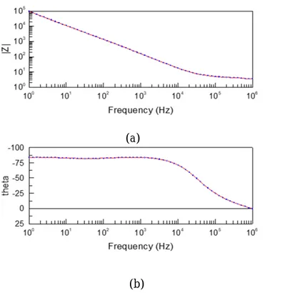
• Bode plot also combined with the plot between theta and frequency can be seen in the following picture. (the following pictures were taken from one of the analysis conducted on the flat aluminium foils etched and anodic formed in house)
The variation of Impedance ( measured in ohms) w.r.t the frequency (measured in Hz), and also the variation of Theta values w.r.t frequencies at different levels, while performing the EIS tests can be observed in the following picture shown below. (See Figure 2 a, b). On comparing the different data of the samples, the curves a&b are generated automatically in the analysis and depending on the values their It is possible to express the impedance as a complex function, where if the
Theoretical Background
steepness increases, fetched from the data analysis done by using the IVIUM software. This is one such kind of a plot which helps in characterizing various kinds of samples and gives an idea about understanding how differently the samples behave with a slight variation in their preparation processes. This plot was used in characterization of various samples in this project at different stages.
Nyquist Plot: This a plot between the real and imaginary parts of the Impedances. This curve is used in assessing the stability of a system. The real part is plotted on the X-axis and the imaginary part is plotted on the y-axis, and the other remaining parameter i.e., frequency (measured in Ohms) is resulting in plot per frequency in this case. Below is an example plot between the real and imaginary parts of the Impedances that represent the stability of the system being measured (See figure 3). Figure 2: General graph generated from the EIS analyses which are usually used to compare the spectra of different samples. (a) The variation of Impedance (measured in ohms) w.r.t the
frequency (b) the variation of Theta values w.r.t frequencies at different levels.
(a)
Theoretical Background
• From the data obtained from the EIS testing, Bode & Nyquist plots are made. The differences between these 2 plots in the point of usage are:
• The frequencies used in Bode plot are explicit but in the Nyquist plot it will not be obvious.
• And small impedances in the presences of larger values of impedances can be identified very easily on Bode plot whereas in the Nyquist plot it’s difficult but by swapping technique the smaller impedance values can be replaced by the larger ones.
• The EIS data or the response of the system being used can be calculated and compared to the actual EIS response of the Electro chemical cells.
The data mentioned above was taken from the Impedance spectroscopy: theory, experiment, and applications [8]
2.6 CPE (Constant phase element)
CPE is an element than can model the double layer of capacitors in an equivalent circuit (a simplest form of the circuit which is represented in the place of a complex circuit which helps in the analysis), and is an imperfect capacitor. The concept of CPE’s is used in the data fitting of the Impedance samples for characterization. The Electrochemical impedance of an oxide layer formation gives us an apparent CPE behaviour in high frequency range and the starting of CPE behaviour is generally attributed to distribution of time constants.
There are two distributions one attribute is time constant along the electrode surface i.e., 2D distribution and the other is time constant normal to the electrode surface i.e., 3D distribution.
The CPE behaviour corresponds to specific behaviour of time constants that may or may not correspond to our physical situation. The CPE behaviour has no physical significance on capacitance value measured in an electric circuit.
Figure 3: A graph generated from the EIS, which related between the imaginary and real parts of Impedance, fetched from the data analysis done by IVIUM
Theoretical Background
The equivalent circuit presented below can be used to represent the electrode in which the interfacial impedance between forming oxide layer and the electrolyte was assumed to be negligible as compared to coating impedance. [9]
Impedance appears as depressed semicircle, like what is obtained for resistance in parallel to CPE. The phase angle is the function of frequency. The CPE exponent alpha is not independent of frequency and approaches a value of unity at large frequencies. [9]
Measurement at different frequencies should ensure that the CPE coefficient is obtained at a frequency larger than the largest characteristic relaxation frequency for the system. By this, the error in double layer CPE coefficient is only one percent. The graphical representation can provide both qualitative and quantitative evaluation of impedance data through Nyquist plot and bode plot. The graphical analysis to obtain values with the impedance of Aluminium foil sample and an oxide covered silver electrode and to simulate an electrical circuit based on the values from R, alpha and Q for the capacitance and CPE behaviour. [9]
In general, the capacitances of a single point can be measured directly, but when considering to measure how the system responds on the internal resistances and how the wide range of spectra differs, the concept of CPE arises. In this, 2 things are varyingly measured which are CPE-P which is termed as
α
and the other is CPE-T which is termed as Q (energy). [9, 13]In the flat foils, after the etching process is done the porosity is considered present in the form of trench tunnels, and as the capacitances of them are measured across all the point of the tunnel, the wide range of spectra is analyzed by CPE-P & T values. [9, 13]
The effective capacitance of the system for a series of capacitors connected can be measured by the formula,
C
eff=
1�𝐶𝐶11�+�𝐶𝐶21�+⋯�𝐶𝐶𝐶𝐶1�
... (11)
In the concept of CPE when being analyzed for a wide range of spectra, it is measured by using the formula,
C
eff=𝑄𝑄
1 ∝(
𝑅𝑅𝑡𝑡𝑅𝑅𝑒𝑒 𝑅𝑅𝑡𝑡+𝑅𝑅𝑒𝑒)
(1−∝) ∝…
(12)From the above equation, the value of Q which is CPE-T can be measured by
calculating all the rest of parameters.
α
in this equation is not CPE-P. In the analysis carried out by KEMET, Granna, the value of CPE-P is obtained directly from the equivalent circuit generated in the analysis software.Interpretation of the EIS Data:
The interpretation of data is dobe to extrapolate
the resistance and the CPE (CPE is proportional to the capacitance, but takes
into account non-idealist of the system)
Theoretical Background
• After the Nyquist plot is made, extrapolation of the semi-circle is done at the right end, to find the horizontal axis.
• Diameter of the semi-circle, extrapolated in the Nyquist plot represents the charge transfer resistance Rf which is equal to the polarization Resistance(Rp) • Larger diameter of the semi-circle represents the higher Polarization
resistance Rp which means the sample being used has a high corrosion (High resistance means High corrosion protection, not corrosion rate) rate. [8,10]
Method and Implementation
3. Method and implementation
In this section we are going to see the process of etching and forming for different industrial samples and in house etched samples.
3.1 Group 1 – in house samples
The process of sample preparation of in house etched samples.
3.1.1 Sample preparation
Firstly, we prepared the samples for performing the Anodic Etching process.
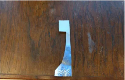
In the first stage of this sample preparation, a thin Aluminium foil is selected and then the samples are made from that. These are made in the flag shaped specimens to easily handle them. Samples of same area of 4 sq.cm were cut out of the flat aluminium foil which can be seen in the picture below. (See Figure 4)
3.1.2 Cleaning procedure
In this process, initially the prepared samples are washed by 3 different solutions to remove any kind of contaminants from their surfaces, as while making the samples they are touched by the lab personnel’s hands. So, the 3 different solutions in which the samples are washed are:
1. De Ionized water.
2. Acetone Solution (99.5%). 3. Ethanol (99.5%).
Method and Implementation
After they are washed in the above-mentioned solutions, they are placed in a glass jar so as to dry them completely. Note that before placing the samples in the jar it also has to be washed in the same way the samples are washed with 3 different solutions. This process of cleaning the samples before performing any experiment is adopted for all the samples before proceeding onto any kind of experiments throughout the project.
3.1.3 Electro chemical etching process Sample Preparation
Note: In the entire project, all the samples which we’ve used we cut of the same area of 4 sq.cm.
Initially 10 flag shaped samples were cut by using the ceramic scissors of 4 sq.cm dimension and named from E1, E2 ...E9, E10. And then the samples were cleaned thoroughly with Deionised water, acetone and ethanol and dried for some time. The sample after washing with different solutions looks like in the below picture,
(See Figure 5).
For making the electrolyte and the set up for the etching process to be carried out we referred to 3 articles where a similar kind of study was conducted as the same as our project. [6, 7, 12]
3.1.4 Pre-treatment
Initially before the samples were processed through the etching process, they were pre-treated with 0.1%wt H3PO4 (Phosphoric acid) which is maintained at 70℃ for 90
seconds.
For this procedure, initially Phosphoric acid of 0.1% wt. is prepared and then it is placed in a beaker and then heated slowly. The temperature to which the acid solution must reach is regulated by the thermostat which is immersed into the acid
Figure 5: Aluminium foil sample of of 4cm2 area which is made ready for the etching process.
Method and Implementation
solution. After the solution reaches as particular temperature of 70℃ the samples will be undergoing the washing process in 3 different solutions and then they are immersed by using a clip into the Phosphoric acid solution for a period of 90 seconds. After this the sample will be immersed into the beaker containing the de ionized water so that any stains of the acid solution on the surface of the samples will be gone away and thereby no extra reaction would be taking place on the surface of the sample.
This procedure is repeated for all the samples and then finally the samples are made ready for the etching process.
3.1.5 Preparation of electrolyte for etching process
For this process as referred from the articles, we initially used the electrolyte of 5M H₂SO₄+1M HCL concentration, but as the samples were of 50 Micron thickness , they were unable to sustain in the etching process for at least 30 seconds and getting burned because it was too high concentration for the of the flat aluminium foil sample. [1]
Here as H₂SO₄ mainly influences the etching process since it is in the higher quantity in the electrolyte, the trails were made by changing the proportion of it in the electrolyte so that an effective electrolyte could be made for conducting the etching process.
So, then another set was made where we reduced the concentration to 2.5MH₂SO₄ and conducted the etching process, but this time the samples were able to withstand till 75 seconds, but still to classify about how different is the etching effect on this kind of flat aluminium foils, the range isn’t enough. And so, we reduced the concentration of the electrolyte finally to 1M H₂SO₄. So finally, the electrolyte which we used for the etching process was 1 M H₂SO₄ + 1MHCl.
3.1.6 Electrochemical etching process
The parameters that were adopted during the etching process were taken from the articles [1, 2] but we changed the composition of electrolyte, temperature etc... Based upon the response of the etching process by trial and error method.
And finally, we set up the parameters as, Temperature of electrolyte is at 70℃, voltage of 4V, current of 150mA/sq.cm, and the etching time was 20 seconds for the first 2 samples, 40 seconds for next 2 samples, and for the final 2 samples it 100 second for the etching process. In total, we made 10 samples. The order we followed is depicted in the following table, (See Table 1).
Method and Implementation
Samples Etching
electrolyte Etching time (seconds) Etching voltage (Volt) Pre-treatment solution Current
(mA/sq.cm) Temp of etching electrolyte (°C) E1 1M H₂SO₄+1MHCl 20 4 0.1%wtH3PO4 150 70 E2 1M H₂SO₄+1MHCl 20 4 0.1%wtH3PO4 150 70 E3 1M H₂SO₄+1MHCl 40 4 0.1%wtH3PO4 150 70 E4 1M H₂SO₄+1MHCl 40 4 0.1%wtH3PO4 150 70 E5 1M H₂SO₄+1MHCl 60 4 0.1%wtH3PO4 150 70 E6 1M H₂SO₄+1MHCl 60 4 0.1%wtH3PO4 150 70 E7 1M H₂SO₄+1MHCl 80 4 0.1%wtH3PO4 150 70 E8 1M H₂SO₄+1MHCl 80 4 0.1%wtH3PO4 150 70 E9 1M H₂SO₄+1MHCl 100 4 0.1%wtH3PO4 150 70 E10 1M H₂SO₄+1MHCl 100 4 0.1%wtH3PO4 150 70
Anodic etching process was conducted making the flat aluminum samples which were pre-treated in the phosphoric acid as anodes and a Silver foil was used serving the purpose of cathode electrode. And then the connections were made and the parameters which were mentioned above were set up for the anodic etching process to be conducted.
After the process of etching is done, the samples are dipped in the de ionized water as before so that the entire electrolyte gets washed away from the surface of the foil and also any precipitates of chloride will be gone away so that no extra reaction would occur on the surface of the foil. And then these samples are kept aside for drying. An aluminium foil after the process of etching is done looks like in the picture
Below. (See Figure 6)
Method and Implementation
Only the flag part of it etched and the rest of it is still a fresh metal.
After the process of etching is done, the capacitances of these 10 samples were measured.
3.1.7 Capacitance measurement
Initially 200ml of working electrolyte Ammonium Adiphate 15% wt. (since Ammonium Adiphate is used as the working electrolyte by the company in their capacitors being manufactured in the company, the same is used here to measure the capacitances), at the room temperature is filled in a beaker and then a long etched Aluminium foil of known capacitance is connected as the positive electrode and for the negative electrode , the sample is held with the negative electrode and only the part of it which has experienced the etching process has to be dipped into the electrolyte to measure the capacitance.
We used an AC signal, at 100mV, and 100 Hz of frequency as the parameters for measuring the capacitances of the samples. These parameters were kept as standard for measuring the capacitances of the samples throughout the project,
The measured capacitances of the etched aluminium samples by following the above procedure are as follows, (see Table 2)
Samples E1 E2 E3 E4 E5 E6 E7 E8 E9 E10 Capacitance(μF) 48 67 200 175 388 380 457 445 503 510
3.1.8 Anodic Oxide forming process Experimental Setup
Ammonium Adiphate Solution (15% wt) should be prepared firstly in which this
Table 2: Showing the capacitances of various etched samples.
Method and Implementation
For this initially Ammonium Adiphate 15% wt should be prepared for using it as an electrolyte. During the preparation, thorough mixing of this solution is to be done so that the salts can get dissolved completely in the de ionized water.
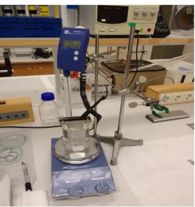
Now the salt solution is to be transferred to a glass jar and the cathode and Anode connections are to be given (A thick aluminum plate is taken as cathode and the etched aluminum foils are connected to be as anode) and the jar should be heated regularly to maintain a temperature of 85℃ (+5 & -2 ℃). A magnetic mixer should be placed inside the solution so that the salt concentration will be distributed equally across the solution.
At their respective voltages of 20,40,60,80,100 V the anodic forming process is carried out by employing the same current of 0.5A (during the setup of the anodic forming process, but when the process of forming starts in the closed circuit after reaching the required voltage the current drops down to a very low value of leakage current)
The parameters required for conducting the anodic oxidation process on the flat aluminum foils were given by KEMET Electronics, Granna, see appendix,1
Reaching of the forming voltage in the closed circuit
In the oxide forming process for the etched samples, the parameters are set as per the requirement, and after this is done, the sample is dipped into the electrolyte and the circuit is switched ON and then it takes time for reaching the forming voltage. In the initial set up when the current is set up to 0.15A there was a long waiting time to reach the forming voltage in the closed circuit. Just for a voltage of 20V it was taking a long time of 20 minutes, and for the rest of voltages it was taking very much long time where the longest was measured as 2.5 hours for 60V.
So, then the forming current was changed to 500 μA and then the time period for achieving the forming voltage in the closed circuit was taking much less time to reach the required voltage in the closed circuit. During the forming process voltage remains constant and therefore current drops down as the oxide grows to the least value but not zero, and this is measured as Leakage current.
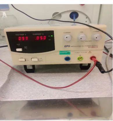
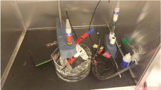
Initially the company suggested to use a current of 0.15A of current, but to achieve this value of current in the closed circuit a very long waiting time was occurring at the voltages beyond 40V. So, the value of current was changed from 0.15A to 0.5A. (This change was made by following the Ohm’s law where voltage is directly proportional to the current). Since using a lower current at the forming process occurring at higher voltages takes a very long time to achieve it in the closed circuit, a little increment in current makes it faster to achieve the forming voltage in a closed circuit. The experimental set up of the anodic oxide forming process can be observed as shown in the picture below. (See Figure.7).
Method and Implementation
After the solution reaches the required temperature the anode and cathode connections are to be given and then for the first sample 20V and 0.05A are to be maintained and then the sample has to be connected as anode. Now the power supply has to be given and the forming process has to be carried out for 10 minutes. After this time, the sample has to be taken out and cleaned with the De ionized water and placed away for drying.
The same procedure has been conducted for the 2nd sample as well. In the meantime, the same volume of solution must be maintained. Because of a high temperature, the water gets evaporated (But not the salt dissolved in it as this temperature is not enough to make it vaporized). So, for maintaining the constant volume of solution De ionized water is added from time to time.
The experiment is repeated for all the samples prepared with different voltages like 40, 60, 80,100 Volts for every 2 samples respectively followed by cleaning with the De Ionized water. The various electrical parameters which are being changed from time to time are done by using the electrical component as shown in the Figure.8 (See Figure.8).
Method and Implementation
The value of the current changes during the forming process but as it is in a very minute level it is acceptable.
Initially we planned to compare the results of both anodic formed foil and etched anodic formed foil, but later as point of usage where the company was focussed is on the etched anodic foils, we decided upon adopting the procedure of anodic etching process first and then followed by the anodic forming process. Which means our work was more narrowed down onto characterising only the anodic etched & formed flat aluminum foils, and not onto the only formed aluminum samples.
3.1.9 Repetition of the forming process
The same procedure of anodic forming was conducted on the industrial samples and also on the samples of 90Microns thickness which were etched industrially. Wherever we used this procedure of forming process all the parameters mentioned above were maintained at their respective forming voltages and the current was maintained as 0.5A.
3.1.10 Heat treatment process
After the process of Forming for all the samples is done, the samples are to be heat treated. For this all the samples are to be placed inside of the Oven at 300±25℃ temperature for a period of 3 minutes. This procedure is done so that any kind of moisture and also the remained residues on the surfaces of the samples would get dried away. Heat treatment process is employed after every etching and forming processes are done on the samples throughout the project.
Method and Implementation
Note: Actually the company uses a higher temperature than the one which we used in our project, it basically uses 500±25 °C for their heat treatment usage, but since in this project the samples which we employed were of lower thickness than the one being used by the company in their production, we reduced the parameter for heat treatment to be around 300 °C.
3.1.11 Separation of samples into 2 groups
Since we made 10 samples (E1, E2, E3,...E10) in number and 2 samples per each condition, we decided to separate the odd numbered and even numbered samples and processed the odd numbered samples through the tunnel widening process where as the even numbered one’s were processed directly to the anodic forming process.
3.1.12 Tunnel widening process
Now among these 10 samples, 5 samples were separated for the tunnel widening process (E1, E3, E5, E7, and E9) and 5 were separates for the oxide forming process. When the tunnel widening was performed in the 3% wt. HNO3 [1], and then the
capacitances of it were measured but unfortunately, they were found to be very low. So, we decided upon to not proceed any further with these samples. These set of samples with their respective capacitances are mentioned in the table below. (See Table 3)
Sample E1 E3 E5 E7 E9
Capacitance(μF) 32 75 96 79 90
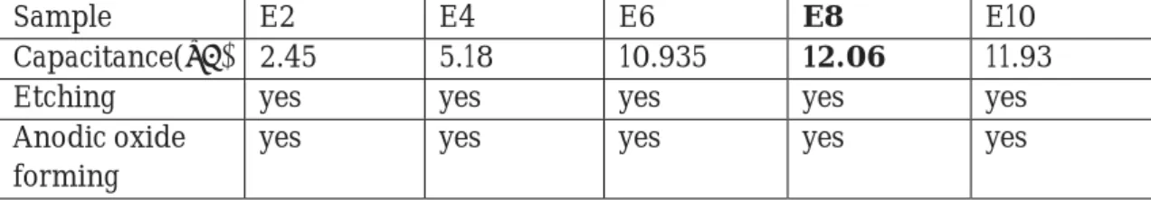
The rest of even numbered 5 samples (E2, E4, E6, E8, E10) were passed onto the anodic oxide forming process at 40V for all the samples. So, we performed the oxide forming process for the above samples at 40V. But as the waiting time for achieving the voltage for the forming process was so long, we decide to increase the current to 500μA so as to reduce the waiting time. And then we measured the capacitances of them at 100Hz of frequency and 100mV level. Entire procedure followed on these samples is depicted in a tabulated form below. (See Table.4)
Sample E2 E4 E6 E8 E10
Capacitance(μF) 2.45 5.18 10.935 12.06 11.93
Etching yes yes yes yes yes
Anodic oxide forming
yes yes yes yes yes
In the above set of samples, the sample with highest capacitance value i.e.; E8 was
Table 3: Showing the capacitances of odd numbered samples after the tunnel widening process.
Table 4: Showing the capacitances of even numbered samples after the anodic oxide forming process is done on them.
Method and Implementation
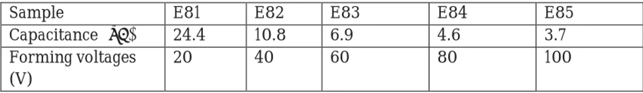
after the attempt of characterizing has made for which we decided upon proceeding with 5 different conditions for forming of the best etched sample. So, 5 different samples (E81, E82, E83, E84, E85) were made based upon taking the condition of etching done on the sample E8 and then these samples are etched and made ready for the anodic forming process at different voltages.
The anodic forming process was carried out on these samples E81,82, E83, E84, E85 at different voltages of 20,40,60,80,100V respectively. The parameters and the electrolyte were maintained the same as mentioned before.
The capacitances of this E8 series of samples after the forming process are found to be as shown with the values in the table below, (See Table 5).
Sample E81 E82 E83 E84 E85
Capacitance (μF) 24.4 10.8 6.9 4.6 3.7 Forming voltages
(V)
20 40 60 80 100
And now after the capacitance measurement was done on all these samples, we proceeded with performing the EIS on the above samples.
3.1.13 Electro chemical impedance spectroscopy (EIS)
After the capacitance check-up was done for the E8 series samples the one’s with the highest capacitances in this group are picked out and then we preceded with them onto the EIS measurements.
When the eis tests were being made we referred to the literature review regarding what an Impedance measurement is and how they are made but regarding the parameters that we followed in conducting them, we didn’t refer to any article in which a particular kind of parameters are used. So, for the first time the following parameters were set (these were set on having a discussion with the company personnel and our thesis project team).
Equilibration time = 300 seconds,
constant potential 2, 4, 6, 8,10V respectively for each time. Frequency = 1Hz to 1,000,000Hz.
Number of points per decades = 31, current range = 100nA. Ammonium Adiphate 15% wt. was used as the electrolyte. These were the parameters which were set for the samples.
In this setup for measuring the Impedance, different electrodes and samples were connected in the following order.
Table 5: Showing the different capacitances of the E8 series samples after anodic forming on them with their respective forming voltages.
Method and Implementation
Flat Aluminium foil was used as a reference electrode (RE). Platinum Electrode is used as a counter electrode (CE).
The sample is made as a working electrode (WE), S was also connected to the working electrode (WE).
Ammonium Adiphate 15% wt. was used as the electrolyte for measuring the Impedance.
After all the above-mentioned things were connected and ensured to be correct, the procedure of EIS was started on the samples E81, E82, E85 at 5 different potentials for each sample.
The kind of procedure which we followed in measuring the Impedance for these samples was used throughout the project on various samples with the same parameters and connections too. But sometimes we change the electrolytes to 7%Boric acid, 1.5% Ammonium Phosphate, 15% Penta Borate. The various samples being used for EIS are placed in the EIS setup according to the Figure 9,
(See Figure 9).
When these tests were being performed, the current must reach to the highest point in the starting and get reduced to the minimum and keep a constant level over the period of equilibration time. But a lot of times a disturbance was being created by the over voltage when the specimens were being run. So, whenever this happens, the equipment is left idle for a certain period and then the tests were being run.
To study the behaviour of electrolyte at the electrode/electrolyte interface we require both potential and current to be monitored. After this step, we have proceeded with observing the micro structures of the samples under SEM.
Method and Implementation
Scanning electron microscope (SEM)
We employed this procedure for observing the morphology of the etched layers on the flat aluminium foils which were having the same etching but the different anodic forming process in them.
For SEM microstructure observation, initially we followed a lot of procedures to observe the micro structure of the etched surface. But finally, we proceeded with fracturing the samples and observing the micro structure of them on the edges under SEM. SEM observation of the E8 series samples was carried out, but as these samples are etched the same so most of the thickness of the porous layer is effected by the etching process and it remains the same on all the samples. But only anodic forming process on these samples is different and so the micro structure observation wasn’t clearly being able to characterize the samples since they all looked the same under the SEM.
The microstructure wasn’t clearly differentiating between the etched layer and the formed layer. And so we proceeded onto analysing the EIS data of these samples.
3.1.14 Updated plan
From the EIS data collected from the E8 series samples we were unable to characterise the different samples since the response of these samples were similar in the system where the analysis was made. The main reason for the response to be similar was that, as the anodic forming process contributed for a very thin layer of material on the etched foil, and so the response of the etched foil at different frequencies w.r.t Impedance and Theta were the same. And so, we were unable to characterise the different conditions.
And so now we proceeded with following a new step of characterising w.r.t. different etching and the same anodic forming process for all the samples which were etched differently. Here etching differently means the only parameter which differs in the etching is the time t. Different time periods were used for different samples. We used the even numbered samples E2,E4,E6,E8,E10 and the anodic forming process was employed on these samples at a same voltage of 40V for a period of 600 seconds on each.
The parameters which we used for all these samples were the same as before except that all the samples were formed anodic at 40V by using a current of 0.5A. All the parameters used could be seen in the table below. (See Table 6)
Method and Implementation
Samples Etching
time(seconds) Forming voltage (Volts) (V) Forming time (seconds) Forming current (Amps) (A) E2 20 40 600 0.5 E4 40 40 600 0.5 E6 60 40 600 0.5 E8 80 40 600 0.5 E10 100 40 600 0.5
After the process of anodic forming was conducted on these samples, they were washed thoroughly in the de ionized water and heat treatment was also done where after these samples were made ready for the EIS check up by using 15%wt Ammonium Adiphate as the electrolyte.
After the EIS was conducted on the above samples at 5 different potentials of 2,4,6,8,and 10V , and the data was collected and the analysis was made on it too and this time were able to get a quality data based on which we were able to characterise the different grades of etching based on the CPE values.
After this step we proceeded onto observing the micro structure of these samples under SEM. For the SEM we fractured the samples and observed the micro structure of the differently etched samples.
3.2 Group 2 –industrial samples (both etched & formed anodic industrially)
Until the above stage, we tried to characterise the different grades of etching, where we have done the etching process in the laboratory, which is In house etching process. But the company purchases the etched aluminium foils from a supplier. But there was no characterization of those samples too. And so we were interested in checking up if the etching produced in house could also give the same result as like that of the samples which were etched and formed anodic industrially.
So, we cut down 3 different industrially etched samples which were industrially etched (we don’t know about the procedure of etching they’ve been done) and formed industrially at voltages 46V, 135V, 374V.
Since the company receives the etched foils in long coils form, the samples were cut in the form of flag shapes. Because of cutting the samples with the scissors, an extra forming process is done on the edges. For each type 3 sample were cut having an area of 4 sq.cm, and all of these samples were formed anodic. For the 3 industrial samples which were formed at 46V, anodic forming was done by using Ammonium Adiphate 15% wt as electrolyte. And as this Ammonium Adiphate 15%wt is high concentrated and so it can’t be used beyond 100V, and so they were formed anodic by using 1.5%wt
Method and Implementation
same parameters as used before when the anodic forming of the in house etched samples was done.
After the process of anodic forming process is done on these industrial samples, heat treatment was done on them and then we proceeded on to EIS for these samples too by using the same parameters as used before at 5 different potentials.
After the EIS was done on these samples, we proceeded to SEM of these samples to characterise them w.r.t the micro structure.
3.3 Group 3 – industrial samples of 90 microns thickness
In this stage, we wanted to compare the characterization of samples in 2 different aspects,
1. A randomly chosen sample regarding which we don’t know any kind of details except that it’s a sample which has been only industrially etched and of 90Microns thick. So, we wanted to check how different would be the response of these samples and compare those results with the in house etched samples and the industrial samples before.
2. Secondly, how different would be the EIS of these samples, when the EIS check-up of them is made by using different electrolytes other than the one in which they are formed (since in the 1st & 2nd stage, we used the electrolyte for both anodic forming process and for the EIS).
So we cut down 20 samples from the long etched foil of 90 Microns thick and then we separated them into 3 different groups. These samples were formed at different forming voltages of 25,46,135,250,375 V in different electrolytes. These voltages were selected since, 25 and 375 are the minimum and maximum respectively of the operating voltages where these etched foil is used in the industrial capacitors.
3.3.1 Set 1: forming anodic in 7% wt. boric acid
5 different samples to be anodic formed at 25V,46V,135V,250V,375V in 7% wt Boric acid using the same parameters as before.
The above group was made to understand how the different samples would react in the EIS. These were named as 25BA, 46BA, 135BA, 250BA, 375BA.
This set is made in order to observe the wide range of response of the etched samples in the EIS system analysis. Entire procedure is depicted in the table below (See Table.7).
Method and Implementation
3.3.2 Set 2: forming in all 3 different electrolytes
In this set we’ve taken 9 samples, which were divided into 3 sub-groups which are to be formed in different electrolytes at 46V using the same parameters as before. Sub group1: 3 samples to be formed in 7% wt Boric acid named as 46BA1, 46BA2, and 46BA3.
Sub Group2: 3 samples to be formed in 15% wt ammonium adiphate named as 46AA1,46AA2,46AA3.
Sub group3: 3 samples to be formed in 1.5%wt Ammonium Phosphate and named as 46AP1,46AP2,46AP3.
Entire procedure followed in this step is depicted in the following table shown below. (See Table.8)
Industrial Samples (90microns thick)
Forming voltage (V)
(volt) Forming electrolyte EIS electrolyte
25BA 25 7% wt Boric acid. 7% wt Boric acid.
46BA 46 7% wt Boric acid. 7% wt Boric acid.
135BA 135 7% wt Boric acid. 7% wt Boric acid.
250BA 250 7% wt Boric acid. 7% wt Boric acid.
375BA 375 7% wt Boric acid. 7% wt Boric acid.
Table 7: Showing the different forming voltages applied on the industrial samples in their respective electrolytes for Forming and EIS.
Method and Implementation
Samples Forming voltage
(Volt) Forming electrolyte EIS electrolyte
46BA1 46 7% wt Boric acid 7% wt Boric acid
46BA2 46 7% wt Boric acid 7% wt Boric acid
46BA3 46 7% wt Boric acid 7% wt Boric acid
46AA1 46 15% wt ammonium adiphate 15% wt ammonium adiphate
46AA2 46 15% wt ammonium adiphate 15% wt ammonium adiphate
46AA3 46 15% wt ammonium adiphate 15% wt ammonium adiphate
46AP1 46 1.5%wt Ammonium Phosphate 1.5%wt Ammonium Phosphate
46AP2 46 1.5%wt Ammonium Phosphate 1.5%wt Ammonium Phosphate
46AP3 46 1.5%wt Ammonium Phosphate 1.5%wt Ammonium Phosphate
For all these samples, the EIS was made under the same electrolyte which has been used for forming process also.
3.3.3 Set 3: forming in only boric Acid & ammonium phosphate
In this set 6 samples were taken and they are divided into 2 sub-groups
Sub group 1: 3 samples formed anodic in 7% wt. Boric acid 375BA1, 375BA2, 375BA3 Sub group 2: 3 samples formed anodic in 1.5% wt Ammonium Phosphate names as 375AP2, 375AP2, 375AP3.
The entire procedure followed is depicted in the table below (See Table 9).
Table 8: Showing the different samples to be formed and EIS to be carried out in different electrolytes.
Method and Implementation
Samples Forming voltage
(Volt) Forming electrolyte EIS electrolyte 375BA1 375 7% wt Boric acid 7% wt Boric acid
375BA2 375 7% wt Boric acid 7% wt Boric acid 375BA3 375 7% wt Boric acid 7% wt Boric acid
375AP1 375 1.5%wt Ammonium Phosphate 1.5%wt Ammonium Phosphate 375AP2 375 1.5%wt Ammonium Phosphate 1.5%wt Ammonium Phosphate 375AP3 375 1.5%wt Ammonium Phosphate 1.5%wt Ammonium Phosphate
Ammonium Adiphate wasn’t used since the concentration of it is so high to be used for forming process beyond 100V.
After the samples are made, firstly for the group 1 samples the EIS was made in Boric acid itself so as to see how the effect is on the samples at wide range of forming voltages from 25V to 375V.
EIS was performed for different samples in all the groups in their respective electrolytes used for the forming process and in same & different electrolytes too for the 2nd group only.
When the EIS was being performed for the samples which are formed with 7%wt Boric acid which were separated into 2nd and 3rd groups, during the equilibration time of the check-up, the procedure was going on stable but when the signal was being applied after the equilibration time, a lot of fluctuations for the current signal being applied were observed. The main reasons for this effect are:
1. Internal resistivity of the boric acid, because of which the electrolyte was being affected when the signal was being applied onto the foil samples.
2. Lack of complete solubility at room temperature, as the boric acid wasn’t dissolved completely in the solvent it was creating fluctuations and so the check-up wasn’t able to be coming out properly.
On observing the above effects, we went ahead with preparing another electrolyte for checking up the samples in EIS setup, which was ‘3 Butyl Amine.’ For preparing this electrolyte, we dissolved 35 grams of Boric acid & 24.5 grams of Tetra Butyl Amine into 500 ml of distilled water. After mixing them well. The mixture was heated up to 70℃, and but the solute tetra butyl Amine wasn’t getting dissolved completely and we were able to see the un dissolved solute clearly at the top of the mixture even though Table 9: Showing the different electrolytes being used for anodic forming and EIS for the
Method and Implementation
the temperatures were raised to certain temperatures. The case of un-dissolved tetra butyl amine solute is found according to the figure 10(See Figure 10).
Since we cannot use the solution which isn’t completely dissolved again, as the same response as above could be expected because of it, we prepared the 15% wt. Penta Borate solution as the electrolyte for the EIS check-up of the industrial samples which were formed in 7% wt. Boric acid in the groups 2 & 3.
The samples of groups 2 & 3, were checked in their respective electrolytes as for forming process firstly, and then to check how the response would be in EIS when the check-up is made under different electrolytes, the EIS of them is made by using different electrolytes too. (This observation is made only for the samples formed at lower voltages and only 2 per each type were chosen, they are:46BA1, 46BA2, 46AP1, 46AP2, 46AA1, 46AA2.)
Here we used naming of samples based upon the voltage used for forming them and the electrolyte in which they were formed. And so,
AA- 15% wt. Ammonium Adiphate AP- 1.5% wt. Ammonium Phosphate BA- 7% wt. Boric acid.
The EIS check-up done on the samples belonging to 2nd set of industrial samples of 90microns thick which are anodic formed at 46V in different electrolytes is depicted in the following matrix, (This matrix explains about if samples has undergone the eis check-ups in different electrolytes, to the left are the samples and to the right in the first row are the different electrolytes and its commented as yes if the EIS check-up was done in that respective electrolyte).
Entire procedure followed in this step is depicted in the table below (See Table 10). Figure 10: Showing the insolubility of solute and the solvent.
Method and Implementation
EIS electrolyte EIS electrolyte EIS electrolyte
Samples AA AP BA
46BA1 Yes Yes Yes
46BA2 Yes Yes Yes
46AP1 Yes Yes Yes
46AP2 Yes Yes Yes
46AA1 Yes Yes Yes
46AA2 Yes Yes Yes
Based on the matrix above used for carrying out EIS in different electrolytes, the analysis of these is made and the characterization of the above samples used on different electrolytes is made and comparison of the results from this set is made with the samples from the stages 1 & 2.
Table 10: Representing the matrix of electrolyte exchange between the different samples formed anodic at 46V.
![Figure 1: A general construction of the capacitors showing the different layers of it, fetched from [3]](https://thumb-eu.123doks.com/thumbv2/5dokorg/4565242.116629/12.892.226.620.718.949/figure-general-construction-capacitors-showing-different-layers-fetched.webp)