Growth of Zinc Oxide Nanoparticles on Top of Polymers and Organic Small Molecules as a Transparent Cathode in Tandem Photovoltaic Device
46
0
0
Full text
(2) LiU-ITN-TEK-A--08/037--SE. Growth of Zinc Oxide Nanoparticles on Top of Polymers and Organic Small Molecules as a Transparent Cathode in Tandem Photovoltaic Device Examensarbete utfört i Elektronikdesign vid Tekniska Högskolan vid Linköpings unversitet. Mohamad Al Kadi Jazairli Handledare Hans Gommans Examinator Mats Fahlman Norrköping 2008-03-05.
(3) Upphovsrätt Detta dokument hålls tillgängligt på Internet – eller dess framtida ersättare – under en längre tid från publiceringsdatum under förutsättning att inga extraordinära omständigheter uppstår. Tillgång till dokumentet innebär tillstånd för var och en att läsa, ladda ner, skriva ut enstaka kopior för enskilt bruk och att använda det oförändrat för ickekommersiell forskning och för undervisning. Överföring av upphovsrätten vid en senare tidpunkt kan inte upphäva detta tillstånd. All annan användning av dokumentet kräver upphovsmannens medgivande. För att garantera äktheten, säkerheten och tillgängligheten finns det lösningar av teknisk och administrativ art. Upphovsmannens ideella rätt innefattar rätt att bli nämnd som upphovsman i den omfattning som god sed kräver vid användning av dokumentet på ovan beskrivna sätt samt skydd mot att dokumentet ändras eller presenteras i sådan form eller i sådant sammanhang som är kränkande för upphovsmannens litterära eller konstnärliga anseende eller egenart. För ytterligare information om Linköping University Electronic Press se förlagets hemsida http://www.ep.liu.se/ Copyright The publishers will keep this document online on the Internet - or its possible replacement - for a considerable time from the date of publication barring exceptional circumstances. The online availability of the document implies a permanent permission for anyone to read, to download, to print out single copies for your own use and to use it unchanged for any non-commercial research and educational purpose. Subsequent transfers of copyright cannot revoke this permission. All other uses of the document are conditional on the consent of the copyright owner. The publisher has taken technical and administrative measures to assure authenticity, security and accessibility. According to intellectual property law the author has the right to be mentioned when his/her work is accessed as described above and to be protected against infringement. For additional information about the Linköping University Electronic Press and its procedures for publication and for assurance of document integrity, please refer to its WWW home page: http://www.ep.liu.se/. © Mohamad Al Kadi Jazairli.
(4) Linköpings Universitet Department of Science and Technology (ITN) . . . Growth of Zinc Oxide Nanoparticles on Top of Polymers and Organic Small Molecules as a Transparent Cathode in Tandem Photovoltaic Device Mohamad Al Kadi Jazairli . IMEC, Leuven Belgium 2007/2008 .
(5) Acknowledgements First of all, I’d like to thank my family and friends for all their support and care, for letting me pursue my interests and be myself no matter the sacrifices or burdens. In addition, I’d like to thank all the staff in the PME group for making imec such a good experience in my life. To all the academics and personnel in the SOLO group: your dedication, knowledge and experience are simply inspirational. Special thanks to my supervisor Hans Gommans, for giving me the chance of exposure to the organic photovoltaic world and being such a humble tutor and person, I can’t thank you enough for your patience, knowledge sharing, advice, and for always being there. Claudio Girotto, Tom Aernouts, and David Cheyns: tons of thanks for all your notes, discussions, and relentless help. I’m also much thankful for the continuous assistance of Jan Genoe, Paul Heremans, Jef Poortmans, and every single person in the group. Last but not least, I’d like to express my gratitude to my thesis examiner at Linköpings University and the director of my masters program Mats Fahlman for his support as well. .
(6) . Abstract . Organic solar cells have caught considerable attention in the past few years due to their potential for providing environmentally safe, flexible, lightweight, inexpensive, and roll‐to‐roll feasible production solar cells. However, the efficiency achieved in current organic solar cells is quite low, yet quick and successive improvements render it as a promising alternative. A hopeful approach to improve the efficiency is by exploiting the tandem concept which consists of stacking two or more organic solar cells in series. One important constituent in tandem solar cells is the middle electrode layer which is transparent and functions as a cathode for the first cell and an anode for the second cell. Most studies done so far have employed noble metals such as gold or silver as the middle electrode layer; however, they suffered from several shortcomings especially with respect to reproducibility. This thesis focuses on studying a new trend which employs an oxide material based on nano‐particles as a transparent cathode (such as Zinc‐oxide‐nano‐ particles) along with a transparent anode so as to replace the middle electrode. Thus, this work presents a study on solution processable zinc oxide (ZnO) nanostructures, their proper handling techniques, and their potential as a middle electrode material in Tandem solar cells in many different configurations involving both polymer and small molecule materials. Moreover, the ZnO‐np potential as a candidate for acceptor material is also investigated. .
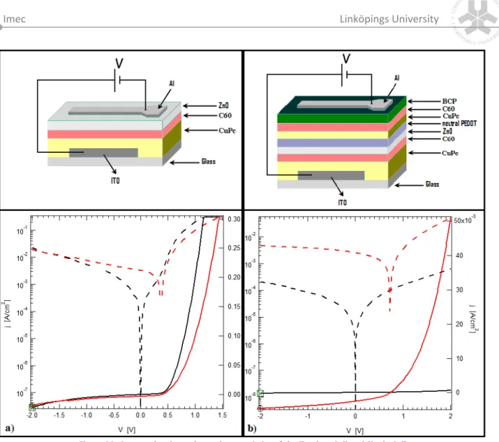
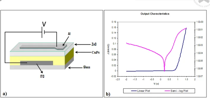
(7) INDEX CHAPTER 1: BASIC DESCRIPTION OF PHOTOVOLTAIC ............................................................... 1 1 INTRODUCTION ..................................................................................................................................... 1 1.1 PV impact on society ................................................................................................................................ 1 1.2 Positioning OPV in PV market .................................................................................................................. 1 1.3 Economical expectations of OPV ............................................................................................................. 2 2 ELECTRICAL CHARACTERISTIC PARAMETER OF THE SOLAR CELL ....................................................................... 3 2.1 Short‐ circuit current ............................................................................................................................... 4 2.2 Open‐ Circuit voltage ............................................................................................................................... 4 2.3 Fill factor .................................................................................................................................................. 4 2.4 Power conversion efficiency .................................................................................................................... 4 2.5 Dark current ............................................................................................................................................. 5 2.6 The Equivalent Circuit Diagram (ECD) ...................................................................................................... 7 3 OPTOELECTRICAL PROCESS IN OPV........................................................................................................... 9 3.1 Absorption of light ................................................................................................................................... 9 3.2 Exciton dissociation‐ Charge transfer and separation of the opposite charges: The heterojunction ... 10 3.3 Charge transport .................................................................................................................................... 13 3.4 Charge collection ................................................................................................................................... 13 3.5 Driving force for directional transport ................................................................................................... 14 3.6 Charge recombination ........................................................................................................................... 16 3.7 An OPV example: The MDMO‐PPV:PCBM blend, its opto‐electrical properties ................................... 16 4 STRUCTURE AND PROPERTY OF TANDEM SOLAR CELL ................................................................................. 18 4.1 Introduction ........................................................................................................................................... 18 4.2 The Middle Electrode ............................................................................................................................. 19 5 ZINC OXIDE NANOPARTICLES SOLUTION ................................................................................................... 20 5.1 Introduction .......................................................................................................................................... 20 5.2 The ZnO nanoparticles as a donor with an acceptor conjugated polymers MDMO‐PPV ................ 21 5.3 The ZnO nanoparticles as a donor with an acceptor small molecules CuPc .................................... 22 5.4 ZnO nanoparticles as a transparent cathode in OPV ......................................................................... 23 . CHAPTER 2: RESULTS AND DISCUSSION ................................................................................. 24 1 SUBSTRATE PREPARATION ..................................................................................................................... 24 1.1 Cleaning process .................................................................................................................................... 24 2 DEVICES STRUCTURES ........................................................................................................................... 25 2.1 Polymer tandem Solar Cell using ZnO nanoparticles solution ............................................................... 25 2.2 Polymer/Organic Small molecules tandem Solar Cell ............................................................................ 29 2.3 Organic Small molecules tandem Solar Cell ........................................................................................... 33 2.4 The ZnO nanoparticles as a donor with an acceptor small molecules CuPc .......................................... 35 3 CONCLUSION ...................................................................................................................................... 36 . REFERENCES: ......................................................................................................................... 38 .
(8) Imec . Linköpings University . Chapter 1: Basic description of photovoltaic 1 Introduction . 1.1 PV impact on society It is expected that the global energy demand will double within the next 50 years. Fossil fuels, however, are running out and are held responsible for the increased concentration of carbon dioxide in the earth’s atmosphere. Hence, developing environmentally friendly, renewable energy is one of the challenges to society in the 21st century. One of the renewable energy technologies is photovoltaic (PV), the technology that directly converts daylight into electricity. PV is one of the fastest growing industries of all the renewable energy technologies [1] . Solar cell manufacturing based on the technology of crystalline, silicon devices is growing by approximately 40% per year and this growth rate is increasing [1]. . 1.2 Positioning OPV in PV market . At present, the active materials used for the fabrication of solar cells are mainly inorganic materials, such as silicon (Si), gallium‐arsenide (GaAs), cadmium‐telluride (CdTe), and cadmium‐indium‐selenide (CIS). The power conversion efficiency for these solar cells varies from 8 to 29%. With regard to the technology used, these solar cells can be divided into two classes. The crystalline solar cells or silicon solar cells are made of either (mono‐ or poly‐) crystalline silicon or GaAs. About 85% of the PV market is shared by these crystalline solar cells [1] . Amorphous silicon, CdTe, and CI (G)S are more recent thin‐film technologies. The current status of PV is that it hardly contributes to the energy market, because it is far too expensive. The large production cost for the silicon solar cells is one of the major obstacles. Even when the production costs could be reduced, large‐scale production of the current silicon solar cells would be limited by the scarcity of some elements required, e.g. solar‐ grade silicon. To ensure a sustainable technology path for PV, efforts to reduce the costs of the current silicon technology need to be balanced with measures to create and sustain variety in PV technology. Therefore, it is clear that implying better solar cell technologies is essential [2] in | P a g e 1 .
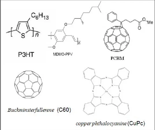
(9) Imec . Linköpings University . the field of inorganic thin‐films, technologies based on cheaper production processes are currently under investigation. Another approach is based on solar cells made of entirely new materials, conjugated polymers and molecules. . 1.3 Economical expectations of OPV . Conjugated polymers and small molecules have the immense advantage of facile, chemical tailoring their properties. Conjugated materials (Figure 1) combine the electronic properties known from the traditional semiconductors and conductors with the ease of processing and mechanical flexibility of plastics. Therefore, this new class of materials has attracted considerable attention owing to its potential of providing environmentally safe, flexible, lightweight, inexpensive electronics. . . . Figure 1: Molecular structures of conjugated polymers MDMO‐PPV, P3HT, PCBM and small molecules C60 and CuPc. . . In the conjugated polymer case, the cost reduction mainly results from the ease of processing from solution. Solution processing requires soluble polymers. Poly[p‐phenylene | P a g e 2 .
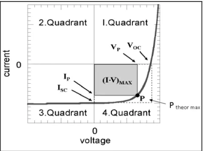
(10) Imec . Linköpings University . vinylene] (PPV, Figure 1) is hardly soluble. Attachment of side‐groups to the conjugated backbone, as in poly [2‐methoxy‐5‐ (3’,7’‐dimethyloctyloxy)‐1,4‐phenylene vinylene] (MDMO‐ PPV, Figure 1), enhances the solubility of the polymer enormously. Furthermore, the nanoscale morphology, affecting the optoelectronic properties of these polymer films, can be partially controlled by proper choice of the position and nature of these side‐groups. Recent developments in ink‐jet printing, micro‐contact printing, and other soft lithography techniques have further improved the potential of conjugated polymers for low‐cost fabrication of large‐ area integrated devices on both rigid and flexible substrates. Architectures to overcome possible electronic scale‐up problems related to thin film organics are being developed [3]. In contrast to conjugated polymers, conjugated molecules are mainly thermally evaporated under high or even low vacuum with the ability of precisely controlling each layer thickness. The necessity for new PV technologies together with the opportunities in the field of organic electronics, such as roll‐to‐roll production, have drawn considerable attention to plastic solar cells in the past few years. Apart from application in PV, it is expected that plastic solar cells will create a completely new market in the field of cheap electronics. . 2 Electrical Characteristic parameter of the solar cell . A solar cell under illumination is characterized by the following parameters: the short‐ circuit current, the open‐ circuit voltage, the fill factor and the power conversion efficiency. In the following paragraphs these parameters are clarified. In (Figure 2) these parameters are indicated on a current‐ voltage curve of a solar cell under illumination. . Figure 2: current voltage curve of a solar cell under illumination with the most important parameters included . | P a g e 3 .
(11) Imec . Linköpings University . 2.1 Short‐ circuit current The short circuit current (ISC) is the current in the illuminated device at 0 V bias. The amount of current is determined by the overlap between the absorption spectrum of the solar cell and the solar spectrum, the intensity of the sunlight, the thickness of the active layer and the excitation/ charge collection efficiency. . 2.2 Open‐ Circuit voltage . The open‐circuit voltage (VOC) is the voltage represents the bias we have to apply in our device in order to decimate the current generated by the illumination of our device. So, at the VOC point there are no external current which flowing through the device under illumination (I=0 A). . 2.3 Fill factor The purpose of a solar cell is to deliver power (current × voltage). The fourth quadrant of the current‐ voltage curve shows where the cell can deliver power. In this quadrant a point can be found at which the power reaches its maximum, called the maximum deliverable power, the maximum power point, versus the theoretical maximum power (Ptheor max), the product of VOC and ISC. . FF =. Pmax Ptheor max. =. I max .Vmax I SC .VOC. It is a measure for the diode properties of the solar cell. The higher the number, the more ideal the diode is. The quality of the diode can be negatively affected by series and shunt resistances, second diode effects and non‐linear effects like bulk and surface injection‐ dependent recombination velocities. . 2.4 Power conversion efficiency The power conversion efficiency (η) reflects how good the solar cell can convert light electrical current. It is ratio of delivered power to the irradiated light power (P light). | P a g e 4 .
(12) Imec . Linköpings University . η=. Pmax I .V .FF = SC OC P light Plight. Since the efficiency is temperature excitation, spectrum and illumination intensity dependent, test conditions were designed to obtain meaningful and comparable values. Standard test conditions include measurement at 25°C under 1000W/m2 of Air Mass (AM) 1.5 irradiation. AM1.5 is the spectrum of the sun (Figure 3), which can be considered to be a blackbody radiator at 5800 k, attenuated for scattering and absorption in the atmosphere. More specially, sunlight attenuated by a travel through 1.5 times the thickness of atmosphere. This is comparable to an insulation at 48.2° from the zenith. . Figure 3: The AM 1.5 solar spectrum with a total irradiation power of 1000 w/m2 . . 2.5 Dark current . The dark current is the current through the diode in the absence of light. This current is due to the ideal diode current, the generation/recombination of carriers in the depletion region and any surface leakage, which occurs in the diode. When a load is applied in forward bias, a potential difference develops between the terminals of the cell. This potential difference generates a current which acts in the opposite direction to the photocurrent, and the net current is reduced from its short circuit value. This | P a g e 5 .
(13) Imec . Linköpings University . reverse current is usually called dark current in analogy with the current Idark(V) which flows across the device under an applied voltage, or bias, V in the dark. Most solar cell behave like a diode in the dark, admitting a much larger current under forward bias (V>0) than under reverse bias (V<0). This rectifying behavior is a feature of photovoltaic devices, since an asymmetry is needed to achieve charge separation. . Figure 4: Current‐voltage characteristic of ideal diode in the light and the dark. To a first approximation, the net current is obtained by shifting bias dependent dark current by a constant amount, equal to the short circuit photocurrent. The sign convention is such that the short circuit photocurrent is positive. . . The net current response of the cell can be approximated as the sum of the short circuit photocurrent and the dark current (Figure 4). This step is known as the superposition approximation. Although the reverse current which flows in response to voltage in an illuminated cell is not formally equal to the current which flows in the dark, the approximation is reasonable for many photovoltaic materials. ‐The ideal diode dark current density J dark =. ⎡ ⎧ ⎛ q(V − JRs ) ⎞ ⎫ V ⎤ ⎟ − 1⎬ + ⎢ J 0 ⎨exp⎜ ⎥ Rs + R p ⎣⎢ ⎩ ⎜⎝ nk B T ⎟⎠ ⎭ R p ⎥⎦ Rp. Where J0 is constant, KB is Boltzmann’s constant and T is temperature in degree Kelvin. The shunt resistor RP (in Figure 5) is due to recombination of charge carriers near the dissociation site (e.g. Donor/Acceptor interface). Provided the series resistor RS is at least one | P a g e 6 .
(14) Imec . Linköpings University . order of magnitude lower than RP, it may also include recombination further away from the dissociation site e.g. near the electrode. Otherwise an extra shunt resistor has to be considered. RP can be derived by taking the inverse slope around 0V: −1. ⎛1⎞ RP ≈ ⎜ ⎟ ⎝V ⎠ This is because at very small voltages the diode D is not conducting and the current driven by the external voltage (positive or negative) is only determined by RP + RS with RP (typically) being much larger. The series resistor RS considers conductivity i.e. mobility of the specific charge carrier in the respective transport medium. For example mobility of holes in a p‐type conductor or electron donor material. The mobility can be affected by space charges and traps or other barriers (hopping). RS is also increased with a longer traveling distance of the charges in e.g. thicker transport layers. RS can be estimated from the (inverse) slope at a positive voltage > VOC where the IV curves becomes linear: −1. ⎛1⎞ RS ≈ ⎜ ⎟ ⎝V ⎠ This is because at high positive external voltages V the diode D becomes much more conducting than RP so that RS can dominate the shape of the IV curve. . 2.6 The Equivalent Circuit Diagram (ECD) A solar cell can be described with a network of ideal electrical components: a current source, a diode, a parallel resistance and a series resistance. The current source represents the photo‐generated carriers. The diode stands for the non linear shape of the IV curve. The parallel and the series resistance shape the ideal diode characteristic into the real diode characteristic from the actual solar cell. These resistances are important since they influence the fill factor to a large extent. A physical interpretation can be assigned to these resistances. The series resistance stands for any factor influencing the carrier movement, e.g. the charge carrier mobility, the thickness of the active layer, contact barriers and contact resistances. The parallel or shunt resistance influenced by charge carrier recombination and shunting paths (paths of high conductivity). | P a g e 7 .
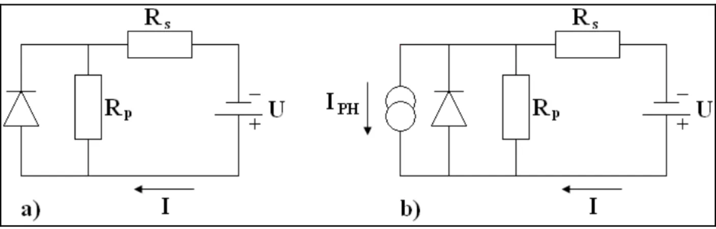
(15) Imec . Linköpings University . . Figure 5: Equivalent circuit for a standard solar cell (a) in the dark and (b) under illumination . These kinds of electronic circuit can also be described mathematically with an expression of the device under dark measurement condition. The following expression equation of the solar cell comes from the ideal diode mathematical expression in which we have added the influence of the Rs and RP. ‐Ideal diode expression: . ⎡ ⎛ qV − JRS ⎞ ⎤ J (V ) = J 0 ⎢exp⎜ ⎟ − 1⎥ nkT ⎝ ⎠ ⎦ ⎣ ‐Expression of the Solar cell: . ⎡ ⎛ qV − JRS ⎞ ⎤ V − JRS J (V ) = J 0 ⎢exp⎜ − Jl ⎟ − 1⎥ + nkT R ⎠ ⎦ ⎣ ⎝ P This last expression is commonly used to describe the performance of all kinds of different photovoltaic devices among which also organic solar cell [3,5]. Upon illumination the light generates a photo current JL that is simply superimposed (added) upon the normal rectifying IV characteristics of the diode D. The addition of JL results in a region of the fourth quadrant where electrical current and voltage can be extracted from the solar cell. The highest voltage in this quadrant develops at the electrodes when JL just manages to cancel the dark current. Thus, given a constant JL the VOC is higher the smaller the dark current is ‐ note that J0 determines the height of the characteristics. | P a g e 8 .
(16) Imec . Linköpings University . 3 Optoelectrical Process in OPV . In general, for a successful organic photovoltaic cell, there are four important physical processes that have to be optimized in order to obtain a high conversion efficiency of solar energy into electrical energy. These are the following: ‐ Absorption of light ‐ Charge transfer and separation of the opposite charges ‐ Charge transport ‐ Charge collection . 3.1 Absorption of light For an efficient collection of photons, the absorption spectrum of the photoactive organic layer should match the solar emission spectrum (Figure 3) and the layer should be sufficiently thick to absorb all incidents light. Electrons from the HOMO level can be excited over the energy gap to the LUMO level by absorbing electromagnetic radiation. Photons with energy less than the energy gap can not be absorbed. In order to absorb in the visible part of the electromagnetic spectrum –extending from 400 to 700 nm‐ a band gap of 3.1 to 1.8 eV is required. Organic semiconductor materials often are fluorescent, a feature which is not observed in the classical inorganic semiconductors. This is caused by the fact that in organic materials the excited states are tightly bound coulombic interaction, whereas in inorganic semiconductors this is generally not the case. In those materials free electrons and holes are generated upon optical excitation. This occurs for two reasons, explained in the following. While most inorganic semiconductors have high dielectric constant (15 is a typical value), organic materials have low dielectric constants (4 is a typical value) causing a large coulomb radius. . rC =. q2 4πεε 0 KT. . Here q is the elementary charge, ε0 the permittivity of vacuum, ε the relative dielectric permittivity of the material, K the Boltzmann constant ant T the absolute temperature. This means that in materials with high dielectric constant the charge are easily screened by the matrix, while in materials with low dielectric constants they are not. This makes that generated electrons and holes can “sense” each other over a longer distance in low dielectric constant | P a g e 9 .
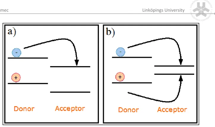
(17) Imec . Linköpings University . materials. In addition, due to the low charge carrier mobility in organic materials the excited electrons and holes are not fast enough to escape the already large Coulomb radius observed in theses materials. Therefore optically excited states in organic materials will be tightly bound and are called excitons. When in inorganic semiconductors like silicon is referred to excitons, those are considered very lightly bound wannier type excitons [4]. The typical wannier exciton binding energy is in the order of 10 meV. Since the thermal energy at room temperature is already 26 meV those will only exist at low temperatures. In organic materials on the other hand, excitons are frenkel type excitons [4] and are located on one molecule. These Frenkel excitons have a strong binding energy, typically in the order of 0.5 eV [4]. It is important to realize that these excitons are so tightly bound they will not spontaneously dissociate at room temperature, nor are the typical electric fields (107V/m) in organic solar cells sufficient to separate the hole and electron of the exciton. Photodetectors (light sensors) on the other hands, typically operated at strong reverse bias (voltage), are able to do this. Hence, a mechanism had to be found to efficiently dissociate these excitons in solar cells. . 3.2 Exciton dissociation‐ Charge transfer and separation of the opposite charges: The heterojunction . The issue of exciton dissociation was solved by adding a second material which is the acceptor material. The material containing the excitons is then called donor material. The acceptor material is chosen on basis of the position of its HOMO and LUMO levels. Both should lie at higher energies (considered from the vacuum level) than the HOMO and LUMO levels of the donor. For the electron of the exciton it is then energetically favorable to jump from the donor LUMO level to the acceptor LUMO level, while the hole will remain on the donor since the jump from the donor HOMO to acceptor HOMO is energetically unfavorable. (Figure 6‐a) This is called charge transfer. In the case where the acceptor HOMO would lie above the donor HOMO, both electron and hole would move to the acceptor and no exciton splitting would occur, but plain energy transfer. (Figure 6‐b) . | P a g e 10 .
(18) Imec . Linköpings University . Figure 6: a) Charge transfer; b) Energy transfer. . . From research in which several donor and acceptor materials were tested a large dependence of the Voc on the acceptor’s LUMO level and the donor’s HOMO level was absorbed [5,6]. The creation of free charge over donor/acceptor heterojunction gives rise to a chemical potential which is the change in free energy of a system when a particle is added or withdrawn, for charged particles this relates to an electrical potential. It is their finding that therefore the maximum open circuit voltage is determined by the energy difference in HOMO level of the donor and LUMO level of the acceptor. During the process of optical excitation the electrons gain potential energy. A part of this energy –the energy difference between donor and acceptor LUMO levels‐ is lost when the electron is transferred to the LUMO level of the acceptor. Therefore it is desirable that the LUMO‐LUMO energy difference is not too much in excess of the exciton binding energy since this results in a loss of VOC. For an efficient charge generation, it is important that the charge‐separated state is the thermodynamically and kinetically most favorable pathway after photo excitation. Therefore, it is important that the energy of the absorbed photon is used for generation of the charge separated state and is not lost via competitive processes like fluorescence or non‐radiative decay. In addition, it is of importance that the charge‐separated state is stabilized, so that the photo generated charges can migrate to one of the electrodes. Therefore, the back electron transfer should be slowed down as much as possible. . | P a g e 11 .
(19) Imec . Linköpings University . The excitons have only limited time before they recombine (typically 10‐9s) and therefore the exciton diffusion length is also limited. Exciton diffusion lengths are typically in the order of a few nanometers [7]. In the case of a planar junction this means only excitons created near the junction are able to reach the donor‐ acceptor interface. Layers with thickness exceeding this diffusion length are in fact useless and are even hampering the device operation du to optical filter effects and due to increasing series resistances in thicker layers. Most of the developments which have improved the performance of organic PV devices are based on D/A heterojunction. The idea is to use two materials with different electron affinities and ionization potential in order to create at the interface an asymmetric potential which may favor the exciton dissociation: the electrons will be accepted by the material with the lower affinity. In order to create the charge dissociation, the differences in the potential energy are larger than exciton binding energy. There are two different kinds of heterojunction (Figure 7), the planar‐ heterojunction (also called bilayer) and bulk‐ heterojunction (also called single layer). . Figure 7: Donor‐ Acceptor principle, (a) bulk heterojunction: 1‐Light absorption and exciton formation, 2‐Coulomb escape, 3‐ electron and hole transport towards cathode and anode, respectively. (b) bilayer heterojunction: 1‐Light absorption and exciton formation, 2‐ Exciton diffusion towards D‐A heterojunction and subsequent charge transfer, 3‐Electron and hole transport through donor and acceptor material, respectively. . . The concept of Bulk Heterojunction (Figure 7‐a) consists on of a blend with donor and acceptor material. The philosophy behind this approach is to bring the interface to the exciton instead of the exciton to the interface. This blend allows increasing the dissociation rate since the length scale of the belt is similar to the exciton diffusion length. Hence, charge generation takes place everywhere in the active layer. | P a g e 12 . .
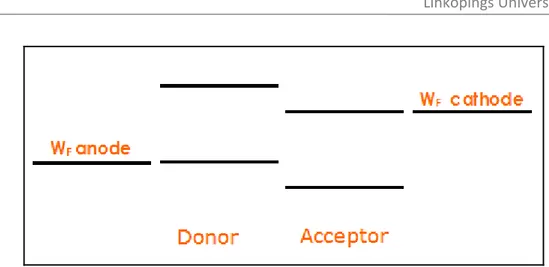
(20) Imec . Linköpings University . 3.3 Charge transport The free charges now have to be transported to the electrodes. Organic crystals have small conduction and valence band compared to the inorganic covalent crystals due the weak van der waals interaction between the molecules. However, it is still debated whether charges can move freely in these bands because of polaron effects. Polarons are charge accompanied by a structural deformation provoked by the generally strong electron‐phonon coupling in organic materials which can hamper smooth charge transport [8]. In disordered organic materials, conduction and valence bands are unlikely to occur and the transport levels rather are defined as a collection of HOMO and LUMO levels. These states are by definition localized and hence the carriers will be localized too. In polymers this means that carriers will be localized on one conjugated segment. Although the mobility of the charges within a conjugated segment can be extremely high (30 cm2/Vs in PPV) [8], the rate limiting step is the movement from one state to another. This is done by so‐called hopping. Hopping transport was found to be temperature and electric field activated. In contrast, band transporters do not show an electric field dependence and have a negative temperature dependence. . 3.4 Charge collection To create a working photovoltaic cell, the photoactive material (D+A) is sandwiched between two dissimilar (metallic) electrodes to collect the photo‐generated charges. The anode collects the positive charges, the cathode the negatives ones. However, under illumination this phenomenon is reversed for some unexplained reason, where the cathode material (at V>VOC) collects the positive charges and the anode material collects the negative ones as illustrated in (Figure 8). . | P a g e 13 .
(21) Imec . Linköpings University . Figure 8: Ideal position of the electrode workfunctions for barrier‐ free charge extraction. . . The basic requirement is to have barrier‐free carrier extraction. This entails the workfunction of the electrode to be as close as possible to the energy level of the charges to be extracted. In the case of the electrons this is at the position of the LUMO level of the acceptor, and for the holes at the position of the HOMO level of the donor (Figure 8). This requires an electrode with a high workfunction for the holes and one with a low workfunction for the electrons. Moreover, in the selection of the electrodes it is important that they are chemically stable. Especially in the choice of the low workfunction metal, which is generally prone to oxidation, this is an issue. Also, one of the electrodes should be transparent in order to enable illumination of the active layer. . 3.5 Driving force for directional transport Until now it was summarized how charges are generated, transported and extracted in an OPV. The force driving the charges to the appropriate electrode remains to be discussed. Traditionally, in semiconductor physics two forces are used to explain carrier motion: drift and diffusion; drift of charges in the presence of an electric field and charge carrier diffusion driven by charge carrier concentration gradients. In the metal‐insulator‐metal model (MIM) [9], the solar cell’s active layer is regarded to be insulating. Insulating does not mean that no conduction of charges is possible; it simply means that very few intrinsic charges are expected. When a semiconductor layer is connected with a metal electrode, the Fermi level of the semiconductor will try to align with the workfunction of the metal. Hereby, a depletion region | P a g e 14 .
(22) Imec . Linköpings University . will be created with the width determined by the number of charges necessary to establish the alignment. . Figure 9: Directional transport in an OPV explained with Metal‐ Insulator‐ Metal (MIM) picture on a I‐V curve of a solar cell under illumination. . . Since in insulating materials virtually no such free charges are present, when sandwiched between two metal electrodes (MIM picture) the insulating layer will be fully depleted and alignation will be obtained between the workfunctions of the electrodes. In (Figure 9) at short‐circuit conductions (zero volt bias), the Fermi levels of the electrodes will coincide and the insulator bands can be regarded as exhibiting a long‐range linearized band bending. Hence, an electric field is present in the entire active layer film. The consequence is that all –optical generated‐ carriers in the active layer will drift in an electric field. Positive charge will be directed towards the anode and negative charges to the cathode. | P a g e 15 .
Figure
+7
Related documents
Both Brazil and Sweden have made bilateral cooperation in areas of technology and innovation a top priority. It has been formalized in a series of agreements and made explicit
The increasing availability of data and attention to services has increased the understanding of the contribution of services to innovation and productivity in
Generella styrmedel kan ha varit mindre verksamma än man har trott De generella styrmedlen, till skillnad från de specifika styrmedlen, har kommit att användas i större
a) Inom den regionala utvecklingen betonas allt oftare betydelsen av de kvalitativa faktorerna och kunnandet. En kvalitativ faktor är samarbetet mellan de olika
Parallellmarknader innebär dock inte en drivkraft för en grön omställning Ökad andel direktförsäljning räddar många lokala producenter och kan tyckas utgöra en drivkraft
Närmare 90 procent av de statliga medlen (intäkter och utgifter) för näringslivets klimatomställning går till generella styrmedel, det vill säga styrmedel som påverkar
• Utbildningsnivåerna i Sveriges FA-regioner varierar kraftigt. I Stockholm har 46 procent av de sysselsatta eftergymnasial utbildning, medan samma andel i Dorotea endast
I dag uppgår denna del av befolkningen till knappt 4 200 personer och år 2030 beräknas det finnas drygt 4 800 personer i Gällivare kommun som är 65 år eller äldre i
